Abstract
This work discusses a novel set of alternate implementations of isolated gate driver circuits for power electronic transistors. The proposed topologies for the driver have been designed specifically for SiC power MOSFET. Three different solutions are discussed, all of them providing the required gate turn-on and turn-off command signal with galvanic isolation, but also supplying power to the secondary side of the driver by means of magnetic transformers. The resulting solutions, all of them implemented with simple circuitry, enable the integration of the driver into the power cell, allowing for theoretical higher power density values in the final system. The principle of operation of the different solutions is discussed, and then the main relevant implementation details are presented. After that, the operation of the circuits is demonstrated experimentally, by testing a set of prototypes of these drivers. This provides a comprehensive design example that assesses the feasibility of the proposed solutions. Finally, the main results of the performance of the three gate drivers, on an SiC MOSFET-based prototype are presented and compared.
1. Introduction
The development of wide band gap (WBG) semiconductor devices has been a major contemporary technological breakthrough, contributing to a revolution in the features of power electronic converters. One of the major trends in power electronics design is the size miniaturization of the converter by increasing the system power density []. This is a critical aspect, not only for restricted space applications, but also for modular-conceived architectures such as multilevel converters. However, it also contributes to increasing the reliability and performance of the overall system, or even for easing the thermal management (generally speaking, thermal issues turn out to be more serious as power density increases) []. A key enabling technology in this miniaturization is the use of WBG devices in power converters.
Silicon carbide (SiC) Metal-Oxide-Semiconductor Field-Effect Transistors (MOSFETs), one of the WBG flagships, are preferred in a number of power electronics applications due to their superior material properties when compared versus other semiconductor technologies, such as Si MOSFETs, Si IGBTs or SuperJunction (SJ) MOSFETs [,,,]. It must be noted that other WBG technologies, such as those based on GaN semiconductors, are also very interesting in terms of performance, and therefore the decision of which transistor brand is the optimal choice for a given application is not straightforward, in most of the cases. However, as a summary of the specific characteristics of SiC, it can be stated that this technology presents [,,,,,,,,,,]:
- Higher system efficiency due to lower switching and conduction losses, because the wider bandgap of SiC (compared to Si) implies smaller leakage currents
- A higher temperature operating range, which implies reduced cooling requirements (e.g., heat sink size); the SiC material thermal conductivity is three times larger than the one found for Si. Moreover, the thermal conductivity of 4H-SiC is higher than that of copper at room temperature, while additionally, its junction temperature can reach values up to 600 °C [,]. However, commercial SiC MOSFETs are still rated at 175 °C due to packaging and reliability limitations.
- A high achievable blocking voltage, because the breakdown field of SiC is about 9–10 times larger than Si [,,].
- A higher switching frequency capability, due to the possibility to reduce the required chip area of SiC around 65 times compared to that of the equivalent Si version for the same current levels. Consequently, a much smaller device parasitic capacitance can be provided [], which yields achieving faster operation speeds (much higher dv/dt and di/dt), thus enabling a dramatic increase in the switching frequency (up to megahertz power converters are foreseen)
The main characteristics of WBG devices have been represented in Figure 1, compared to those of Si. This plot depicts physical parameters such as the thermal conductivity, λ, the melting point, TF, the breakdown electric field, EBR, the bandgap energy, E, and the electron saturation speed, Vs. It can be seen how WBG performance stands out as compared to Si-based power devices in the magnitudes related to operating temperature (λ and TF), to voltage ratings (EBR) and to switching frequency and losses (E, VS).
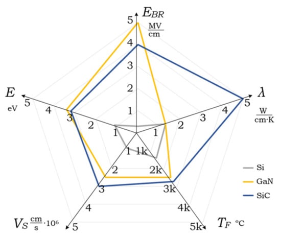
Figure 1.
Main characteristics of different semiconductor materials (Si, SiC and GaN) [,,,,,,,,,,].
The highlighted properties of SiC MOSFETs and their adequate implementation in the system lead to a dramatic reduction in losses and to a significant increase in power density []. Examples of SiC-based devices are both the SiC power Schottky barrier diode (SBD) and the SiC power MOSFET. SiC SBDs are faster than PiN diodes, due to the lack of reverse recovery current at turn-off (because no minority carrier recombination is present, unlike in the standard PiN diode). However, no feasible Si SBD power devices are found for the voltage levels required in typical power electronic applications. On the other hand, the ten-fold higher blocking field of SiC materials makes SiC SBDs a more practical solution for power diodes. Thus, the efficiency increases significantly compared to the standard Si-based diode applications [,,]. On the other hand, due to the high breakdown electric field in SiC, the SiC Power MOSFETS devices admit more doping for the same final blocking voltage than in Si-based switches, implying a reduction in the on-resistance []. Moreover, the effect of hard switching in topologies such as the H-bridge inverter, are also dramatically decreased by pairing these devices with an SiC Schottky diode [,].
Currently, SiC solutions have been on the market for over a decade, and the technology is reaching maturity. Hence, a wide range of devices based in SiC can be found on the market [,]. The higher operating voltage and switching frequency ratings of SiC devices expand the design specifications and the applicability limitations of power electronic converters based on this technology. In practical designs, GaN devices provide very high switching speeds and they are available up to 600 V. However, SiC is currently available up to 1.7 kV commercially, for high power ratings compared to GaN. Figure 2 shows the operational margins in general converter applications, and classifies the main power semiconductor technologies as a function of power level and switching frequency [].
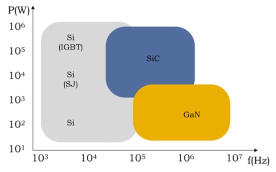
Figure 2.
Main application power and frequency ranges as a function off the power semiconductor technology (Si, SiC and GaN) [].
However, these developments present specific challenges in the system, such as the optimization of the reactive components for higher frequency and high temperature operation, the development of protecting circuitry, packaging, and so on [,,,,,,]. A major issue among these challenges is the design of the gate driver required for an optimum control of the power MOSFET. The design of the driver needs to satisfy its operational requirements. In order to do so, the relevant, distinctive features of the SiC MOSFET, compared to Si IGBT, need to be established [,]. The key characteristics to be considered in the design of the driver can be summarized as []:
- Transient features of the power device, such as the turn-on, ton, and turn-off, toff, switching intervals, as well as the rise and fall time intervals, tr and tf, respectively, which are much faster than in the case of standard drivers for Si devices. Additionally, the propagation delays with increased switching frequency need to be considered in SiC-based power converters []. As a main requirement, the gate voltage of the SiC MOSFET must have a fast dv/dt to achieve fast switching times. This indicates that a very low impedance driver is necessary [,]. For instance, if an optocoupler is used, it must provide a high common mode transient immunity (CMTI) [].
- Static features of the SiC MOSFET, such as the drain-to-source on-resistance, RDSon, that determines the gate-to-source voltage, vGSon, when the device is turned on.
- The required driving voltage levels for the power MOSFET; in case of an SiC driver, the most suitable values are defined as []:
Specifically, for vGSon, even though the switching losses and the switching times decrease for higher voltage levels, such gate stresses might yield premature malfunction, therefore affecting the device reliability [].
- The total gate charge of the power device. This parameter is significantly lower in the case of SiC MOSFET.
- The parasitic capacitances of the power device. Some complexity is imposed by the turn-on and off events due to several nonlinear parasitic capacitances that affect the process. These capacitances depend on the operating conditions of the device. Moreover, these values are coupled with the conditions at the gate drive []. Therefore, the study of the switching waveforms in SiC is critical for understanding the requirements for the gate driver, particularly for very fast drivers []. However, the measurement and characterization of these components, specifically the SiC MOSFET capacitances, is not straightforward in most cases [,,].
- Implementation and hardware design of the gate driver. These aspects determine key parameters such as the gate resistor, the parasitic inductances (dictated by the gate driver layout and connection to the gate terminals of the SiC MOSFET), which can cause false turn-on and turn-off instants during switching transitions, and increase switching losses and shoot-through related failures in the converter [,]. On this basis, a complete analysis of current-controlled and voltage-controlled drivers for SiC MOSFETs is presented in []. In particular, the trends for the gate driver and the protection circuitry are to integrate these features into a single-chip solution. In this case, the major challenges arise due to the resulting high di/dt and dv/dt. Additionally, the noise susceptibility is a critical issue in polluted electromagnetic (EM) environments []. The driver must be designed considering the relatively low parasitic values of inductance and capacitance that arise from the packaging conditions in SiC devices. This parasitic reduction requires that driving and sensing circuits must be as close as possible to the WBG switching devices. Some solutions propose such levels of integration [,].
The objective of this work was to develop a set of self-supplied gate drivers with galvanic isolation, which can be used for various topologies with different voltage ranges. Specifically, this research targets implementations that enable the integration of the driver into the power module, thus allowing for a theoretical higher power density values of the final system. The present work describes in detail the characteristics and operating principles of a set of proposed drivers, presents the full dimming range operation through experimental results, and finally carries out a comparison of the three drivers in terms of operating constraints, size and cost. The novelty of the work can be summarized as the proposal of novel topologies for the implementation of the self-supplied isolated gate drivers for SiC MOSFET switches, the detailed description, analysis, design procedure and validation by simulation and experimental results of these proposal, and a critical analysis and comparison of the performance of the proposed solutions.
The following sections of this paper are organized as follows. Section 2 elaborates a deep analysis of the technical literature related to the state of the art of gate drivers, discussing the main aspects for the design of drivers for SiC power MOSFET switches. Additionally, this section introduces the strategies implemented in the solutions proposed in this research. Section 3 describes the operating principle of a driver based on an impulse transformer, shows the different functional blocks of the device, and describes the theoretical waveforms expected. Section 4 discusses the implementation of these constructing blocks with real circuits and verifies the operation principle through simulations. Later, Section 5 presents the built prototypes of the driver, shows the characteristic waveforms that validate the proposed operating principle, and also states the operational constraints of the solution. Section 6 describes the theoretical driver based on the HF on-off modulation scheme, while Section 7 addresses the validation through simulations of this circuit. Section 8 shows the built prototype and the experimental results found. Section 9 and Section 10 focus on the single transformer modulated driver and define the operating principle, and present the theoretical waveforms expected, respectively. Section 11 covers the validation of this proposal, dealing with the implementation of the bi-level modulated driver prototype, and validates its operation experimentally. Section 12 carries out a comparative analysis of the three drivers in the family, and finally Section 13 discusses the main conclusions of the research and proposes future developments.
2. Analysis of the Technical Literature in the State of the Art
Based on the above discussion, the specific parameters that need to be taken in into account in the design of a gate driver circuit can be analyzed and discussed. A basic circuit of the main elements involved is shown in Figure 3, for the case of the inductive switching of a MOSFET. The following paragraphs summarize the major design aspects in a driver for SiC power MOSFET devices.
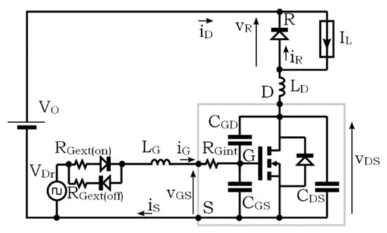
Figure 3.
Diagram of a MOSFET driver in the case of inductive switching.
2.1. Resistance of the Driver, RG
The rise and fall times of the SiC device are limited by the impedance in the gate loop, which usually can be simplified to a series connection of the gate resistance and the parasitic inductance [,]. Therefore, this output resistor needs to be defined accordingly. However, it must be noted that the gate resistor, RG, is generally composed of two elements—the driver gate resistor, RGext, and the internal gate resistor, RGint, of the power device:
This parameter must therefore be considered in the circuit design []. Generally speaking, the smaller the RG, the faster the switching. In fact, RG reaches a minimum value by making RGint = 0. However, this provides EMI issues and stresses the gate much more []. On the other hand, the larger the RG, the smaller the peak driver current, consequently limiting the switching speed. It also can be stated that the larger the RG, the smaller the ringing voltage at vGS [,,,,].
2.2. Parasitic Capacitances
The values of the parasitic capacitances of the device, CGS, CGD and CDS, must be considered. In some configurations, the high switching speed can trigger resonances formed by the parasitic capacitances along with the parasitic elements of the circuit []. This can lead to modulating the gate voltages and potentially triggering undesired switching of the device []. The gate resonant circuit is formed by the SiC MOSFET input capacitance, the gate wiring inductance (gate and source inductance), and the gate resistance (external gate resistance, intrinsic MOSFET gate resistance and intrinsic gate driver resistance) [].
2.3. Parasitic Gate Loop Inductor
In order to decrease the gate loop inductor, LG, the driver must be located as close as possible to the device []. Additionally, specific configurations such as the Kelvin source connection can be used. Reducing the stray inductance with proper layout is the best means to minimize the ringing []. Using accurate models of the SiC MOSFET, an initial design for the driver can be accomplished [,]. The external parasitic inductances of the tracks (typically around 20 nH) should also be considered for the design []. Another model including the inductances is presented in [], while the power losses can also be modeled through analytical expressions [].
2.4. Isolation Requeriments
Most of the driving circuits need galvanic isolation in order to meet the operating specifications required. For this purpose, two main techniques are implemented: optical isolation and magnetic isolation. As a general statement, it can be said that magnetically isolated drivers are usually simpler, faster, and suitable for high temperatures []. However, this assertion needs to be discussed thoroughly, because it depends critically on the application considered.
2.5. Derivative of Voltages and Currents, dv/dt and di/dt
The high-speed switching of SiC devices implies a high dv/dt. Such voltage variations at the gate-to-drain capacitance induce significant currents through the gate, which must be provided by the driver. If the gate-to-source capacitance is too large, these currents might cause spurious turn-on of the device, yielding to destructive shoot-through [,,,,]. Related to this point, high dv/dt immunity must be ensured. This turns into a critical issue in the case that galvanic isolation is required. If an isolation transformer is included in the driver, then the inter-winding coupling capacitance should be essentially taken into account []. In the case of using optocouplers, the CMTI is also a key parameter to take into account [,]. Some extra features can be considered for high performance applications. Among these features, the identification of gate charging sequence enables enhanced control techniques for turn-on and turn-off of the SiC MOSFET driver. Thus, the dv/dt in vDS and the di/dt at iD can be independently controlled, enabling for an optimal switching in terms of losses and EMI issues []. Other options for decoupling these slopes are through optically control []. Additionally, a dynamic adaptation of the driver current to the operating conditions can increase the efficiency or enhance dv/dt performance []. Finally, the values of dv/dt and di/dt of the driver can also be calculated from the parameters of the device to control [,,].
2.6. Tolerances
The effect of tolerances and mismatch of parameters of the SiC affects the paralleling and series operation of these devices [,,,,,,,,]. The gate parameter variance among multiple samples of same device is presented in ref [].
2.7. Packaging
Packaging of SiC MOSFET has a strong influence on the actual device performance in the converter, because the packaging dictates system layout and integration, and therefore electrical and thermal performance. In order to minimize a number of the aforementioned effects, a specific scheme of pairing the drive to the particular device might be considered. In this case, the driver can be included into the same packaging of the power device []. To withstand the same conditions as the power device, in terms of thermal and electric performance, the driver must also be implemented in SiC [].
The analysis of the state of the field reports a number of existing solutions in the technical literature. These solutions address the main distinctive features in the switching phenomena found in SiC MOSFET devices [,,,,,], that have been discussed above. Some authors propose active gate drivers, which allow for varying the total gate resistance of the driver, RG, to be considered as one of the most promising techniques []. Some other authors explore dynamic gate resistance modulation techniques, in order to keep the SiC devices in safe operating ranges, although ensuring low losses and low voltage and current overshoots [,]. The effects of a dynamic control of the driving voltages, vDRon and vDRoff, are explored to minimize the dv/dt and di/dt in the power device, thus addressing overshoot, oscillation, and EMI issues []. Additionally, some researchers have explored the effect of dead times in the performance of the system formed by the SiC MOSFET and the driver []. Authors in [] investigated the reduction in the parasitic gate loop inductor LG when the driver was integrated into the power device package. This analysis has shown interest in the research field in terms of the design of drivers for SiC power MOSFET devices. These drivers need to fulfill, as a general set of features, a high reliability, high power density, high frequency (HF) operation, galvanic isolation, and full-range Pulse-Width Modulation (PWM) duty ratio operation [,,,,,,,].
In the particular case of isolated drivers, the first thing on which to focus is the strategy for the effective transfer of the gating signals and the power required for the adequate switching of the MOSFET with the required voltage isolation. In this sense, by far, most implemented solutions make use of an optocoupler device to transfer the gating signal, along with an independent isolated power source, with its secondary output referred to as the source terminal of the MOSFET, to supply the energy demanded by the high-power side of the driver [,,,,,,]. This standard solution generally involves a significant physical area in the printed-circuit board (PCB) design of the converter and reduces the power density of the system []. Even though it is a robust, well-known, state-of-the-art solution, this approach has several drawbacks, mainly coming from the parasitic elements that both the optocoupler and the dedicated power source present between the primary and secondary sides of the driver. These parasitic elements imply high circulating currents and large induced voltages in the gating loop, that significantly increase the susceptibility to moderate dv/dt values in the system, leading to undesired turn-on/off events and, eventually, to reliability concerns [,,,,,,,]. Additionally, a widespread solution is the implementation of isolated drivers by using pulse transformers by means of magnetic cores. These transformers have the main drawback of core saturation, especially when used in variable duty ratio applications. Most of these drivers operate well only for a narrow margin of duty ratio values, thus limiting their applicability [,]. To avoid the core saturation issue, the typical solution for other applications consists of including a series capacitor to block the DC components. However, this solution limits the bandwidth of the driver, because it implies transient fluctuations on the transformer waveforms when fast transitions in the duty ratio are required. Besides, the secondary side waveforms are also affected, and complex reconstructing stages are needed in order to restore the original gating signal. Therefore, the design of such magnetic-based driver circuits needs to consider the saturation limitations, the wide-range duty operation, and the dynamic response.
Another solution found in the literature to avoid magnetic core saturation is the use of symmetric pulse operations for turn-on and turn-off. The fundamental problem with these solutions is the limited duty cycle operation range. Limited duty cycles make these solutions impractical, because keeping power MOSFETs fully on or off during stand-by or fault conditions needs to be avoided [,,]. Finally, there is another design methodology for magnetically isolated drivers that avoids the saturation phenomenon by using modulation strategies for the turn-on and turn-off of the power device [,,,]. The modulating frequencies implemented in these solutions range from hundreds of kHz up to several MHz. For the former relatively small modulating frequencies, square waveforms can be used as the modulating signal. However, the efficiency of the driver stage is limited due the hard switching in the oscillator stage. In the latter case, the state-of-the-art implementation includes resonant tanks. These resonant solutions need to cope with the required control schemes to ensure resonant operation of the circuitry under all possible conditions, but also with synchronization issues, limited dv/dt aspects in the demodulation blocks, effects of the coupling parasitic elements, etc.
Besides the solutions discussed in the previous paragraphs, Table 1 summarizes additional research reported in the literature for WBG isolated drivers, sorted by the main topic covered.

Table 1.
Additional state-of-the-art solutions for isolated gate driver circuits for wide band gap (WBG) devices.
To overcome the reported issues in the performance of gate drivers for SiC, this work proposes a family of isolated gate drivers for SiC power MOSFETs. The aim of the research was to propose, validate, and compare driving solutions that avoid the use of the dedicated isolated DC-DC power source that delivers the power demanded by the secondary side of the driver. The first driver topology of the proposed gate driver family is based on an impulse transformer, which transfers the information of the turn-on and turn-off instants to the secondary side of the driver []. An ancillary circuit reconstructs the gating signal, and also provides the required power levels for triggering the power MOSFET. In order to solve the limit of applicability and the operational constraints of the impulse transformer circuit, an alternate solution based on an HF on-off modulation of the signal is delivered to the primary side of the driver transformer [,]. This solution requires an additional transformer for supplying the required power in the secondary side. Finally, a driver based on a dual level HF amplitude modulation (AM) scheme, applied to a single magnetic transformer will be introduced. This single device simultaneously provides the triggering turn-on and off signals for the target device, but also the amount of power required to effectively drive the gate at the secondary side. A preliminary version of this proposal was introduced in [,] for SiC MOSFETs, and in [] for GaN power devices.
3. Description of the Driver Based on the Impulse Transformer
The first idea is to use a single isolation component, in this case a magnetic transformer, in order to simultaneously send the gating information (turn-on and turn-off signals) and the required power to effectively turn the power device on and off. The basic diagram block of the driver is shown in Figure 4. The gating signal is a rectangular waveform generated in the digital signal processor, in particular using the dedicated PWM block generator of the controller. This signal generates a pulsed voltage waveform, vp, which has the peak and valley levels corresponding to the voltage supply of the primary side, vCC, and ground, GND, of the signal controller. The duty ratio, d, of the signal, can be defined as the ratio of the turn-on time, d·T, and the full switching period, T. This signal vp is sketched in Figure 5.
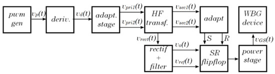
Figure 4.
Block diagram of the driver based on a single impulse transformer.
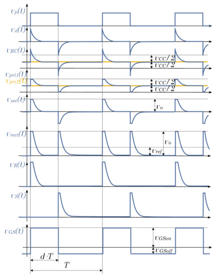
Figure 5.
Theoretical waveforms in the driver based on a single impulse transformer.
Even assuming an adequate matching of impedances and a sufficient power level, if such a signal vp is directly applied to the primary side of the transformer, taking into account that vp inherently includes a DC component, it is obvious that the transformer operating conditions will eventually become saturated, yielding a malfunction of the system. In order to avoid the saturation of the core, the proposal opts to provide a processed signal from the original waveform, by means of a derivative block that generates the pulsed waveform vd. As it can be seen in Figure 5, the pulsed signal has a null average voltage value. This ensures an operation free of saturation in the transformer, independently of the duty ratio of the signal considered. However, the gating PWM signal needs to be reconstructed in the secondary side, by ensuring the required voltage values and the adequate power levels. In order to achieve this, the derived signal is adapted to enter the primary and secondary sides, by boosting its power levels by using an adapting stage. This stage generates the voltage signals at the primary side of the transformer, vpri1 and vpri2, with adequate voltage and power levels. The secondary side terminals are connected to a stage that rectifies and filters the secondary waveforms, vsec1 and vsec2, to generate the secondary side supply voltage, vO. This stage also generates a reference voltage, vref, that will provide the final asymmetrical vGSon and vGSoff levels.
By observing Figure 5, it can be seen how the secondary side signals vsec1 and vsec2 can be processed to trigger the turn-on and turn-off instants. The followed strategy is to generate, from these waveforms, set (vS) and a reset (vR) input signals for an RS flip-flop, that reconstructs the original gating signal. This block has been implemented by means of an operational amplifier (OA). A final power stage is in charge of shaping the digital gating signal to the final output values, and also to inject the required power by amplifying the output drive current.
4. Main Characteristics of the Impulse Transformer
As a result of the working philosophy sketched above, two impulses with opposite polarities are sent to the secondary side per switching period. Given that these pulses are rectified to generate the secondary side power supply, it is clear that the absence of these pulses prevents the operation of all the secondary side blocks. This implies that this driver cannot operate in the case of a fully turned-on (duty to 100%) or fully turned-off (duty equals 0%) switch command. This latter aspect may not result in a critical issue; the resulting voltage with 0% duty ratio will obviously be 0 V, resulting in a constant turn-off of the switch. However, it is true that a 100% duty operation (e.g., switch continuously turned on) is not possible with this approach, resulting in the most important limitation of this solution. In the real application, the limit values achieved are 10–90%, and the system can easily be adapted to provide 0–90% operation. The next subsections discuss the implementation, with analog circuitry, of the construction blocks sketched in Figure 4.
4.1. Implementation of the Working Principle
The working principle is founded in the derivation of the primary side voltages for the transformers from the initial PWM signal, vp. This derivation is carried out by means of a simple RC network, labelled as deriv in the diagram of Figure 6. The output of the RC network, vRC, is amplified by a power stage, implemented by means of a Bipolar Junction Transistor (BJT) complementary stage. The output of this stage, vpri1, is connected to one of the primary side terminals of the transformer. In order to attain an adequate operation of the complementary stage, the derived signal vRC must actually be biased to vCC/2, which is achieved by referring the derivative resistor, R, to a voltage divider rather than directly to the ground. In addition, this bias level is connected to the remaining primary side terminal, vpri2, in order to ensure a saturation-free operation of the transformer. The biasing of the derived signal, however, has further implications in the design procedure. As is depicted in Figure 5, the derived signal vRC should reach +vCC and −vCC in the positive and negative edges, respectively. When the +vCC/2 bias is included, it should reach +3vCC/2 and −vCC/2, respectively. However, at the output of the BJT stage, vpri1, is clamped at vCC and 0. This condition is imposed by the diodes in the junctions of the complementary NPN and PNP BJTs. The clamping phenomenon determines the width of the pulse that is effectively employed for transferring energy to the secondary side, and it is given by the time constant, RC, of the derivative network. Therefore, RC is a design parameter for tuning the width of the pulse for power transfer. Hence, the wider the pulse, the smaller the required current for the same amount of power delivered to the secondary side, resulting in a decrease in losses and, therefore, in an increase in the efficiency. However, large time constants in the derivative network also imply that the derived waveform loses symmetry with respect to the voltage levels for small duty ratio, thus imposing a DC component in the primary side that may saturate the core. Therefore, the final RC value needs to be defined as a trade-off between efficiency and minimum duty ratio achievable.
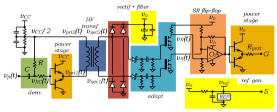
Figure 6.
Detailed diagram of the driver based on the impulse transformer.
4.2. Characterization of the Impulse Transformer
In order to define the turns-ratio of the transformer, the required voltage values at both the primary and the secondary side must be established, taking into account all the parasitic elements and the non-ideal components in the parts involved. The AC voltage waveform at the primary side has a peak value that can be represented as:
where vCC stands for the primary side supply voltage, and vBE and vCE are the base-to-emitter and the collector-to-emitter saturation voltage of the BJTs at the complementary power stage in the primary side of the transformer (see Figure 6), respectively. The peak value at the secondary side voltage needs to also consider a number of elements in the circuit, as shown in Figure 6:
where vF is the forward voltage drop in the rectifier diodes at the bridge at the secondary side, vRail is the difference from the supply voltage to the output voltage at the OA, and vBE and vCE are again the base-to-emitter and the collector-to-emitter saturation voltage of the BJTs at the complementary stage, respectively. Equations (4) and (5) are the expressions for the turns-ratio in the transformer:
The second basic requirement in the design is the value of the magnetizing inductor of the primary side, that can be defined considering the operation of the transformer. It is assumed that the impedance of the magnetizing inductor, ZLµ, needs to be significantly higher than that of the secondary side, Z′sec, as seen by the primary side:
where Lµ is the magnetizing inductor of the transformer at the primary side.
The value of Z′sec can be estimated by assuming the power consumption at the secondary side, Psec, and the RMS voltage at the primary side of the transformer, vpri(RMS). Given the voltage shape at the primary side (see Figure 5), a form factor, FF, can be used for this definition. This value depends on the RC time constant of the derivative network:
The value of Z′sec can be estimated by:
Therefore, the design condition for the magnetizing inductor at the primary side is:
Equations (6) and (10) determine the input parameters in the design of the transformer.
4.3. Generation of the Output Votage Levels
The supply voltage at the secondary side, vo, is obtained by rectifying and filtering the secondary side voltage, vsec. This value is ensured with the turns-ratio obtained from (6). The adequate supply of the power MOSFET implies a non-symmetric voltage drive, given by vGSon and vGSoff. In order to attain the adequate negative bias in the output voltage pulses, a voltage reference integrated circuit is needed which ensures a stable negative vGSoff voltage level.
4.4. Implementation of the Reconstructing Stage
The reconstructing stage is based on the use of a SR flipflop, that will be triggered by the rising edges in the secondary side terminals of the transformer. This edge-triggered flip-flop is implemented by means of two derivative networks that adapt the waveforms at the secondary side, followed by a rail-to-rail OA (see Figure 6). The output of the OA, attached to a BJT complementary power stage, provides the output waveform with the required levels to drive the power MOSFET. Therefore, the gate loop is formed by the external resistor Rgext, the OA + BJT complementary stage at the gate terminal, the capacitor in parallel with the voltage reference IC at the source. This capacitor has a large capacitance, which is implemented with an electrolytic device in parallel with a ceramic capacitor, in order to avoid any issue at HF operation.
4.5. Circuit Modeling and Simulation Results
A complete circuit of the driver, sketched in Figure 6, has been implemented in LTSpiceTM. This software allows for a complete modeling of all the parts in the circuit, including the parasitic components and the non-ideal parts. Table 2 shows the specific part references chosen for the components depicted in Figure 6 for the implementation of the driver prototype. The values of the parameters involved in the design of the transformer are given in Table 3.
Table 2.
Commercial parts to implement the driver based on the impulse transformer.
Table 3.
Design parameters for the calculation of the transformer.
With the parameters in Table 3, the main design parameters for the transformer can be obtained from (6) and (10):
It must be considered that, in order to ensure adequate operation of the transformer, the condition in the inequality in Equation (10) has been guaranteed by taking a factor of 20 for the final value of Lµ.
A set of simulations has been carried out to further design the rest of elements in the driver. Figure 7 shows the simulated waveforms for a 50% duty ratio pulse signal, switching at 100 kHz. It can be seen how the derived waveform is measured at the primary side of the transformer, and how the pulsed waveform is transferred to the secondary side. The terminals at the secondary side also provide the set and reset signals for the analog edge-triggered flip-flop. The final voltage at the gate of the SiC Power MOSFET reaches the target values of +20 V/−5 V.
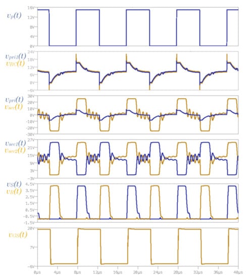
Figure 7.
Main waveforms in the impulse-based driver (Simulation in LTSpiceTM).
5. Experimental Validation of the Driver Based on the Impulse Transformer
However, the simulation only provides a partial validation of the operation of the driver. Aspects such as the full model of the transformer or details in the functional limitations of the circuit can only be assessed by constructing a laboratory prototype of the driver. Figure 8 shows the actual prototype of the driver. The initial design of the impulse driver presents a layout area of 82 × 19 mm2. The transformer has been implemented in a toroidal core, and the primary (left) and secondary (right) sides of the driver can be clearly identified. The design of the magnetic element has been carried out from the design constraints in expressions, and also following the procedures and the Design Tool SFDT given by the manufacture of the toroidal core, FerroxcubeTM []. Two devices were built, in order to test the operation of the driver in a bidirectional DC-DC buck-boost converter (see the main characteristics given in Table 4). This converter is implemented using C2M0080120D SiC Power MOSFET, from Wolfspeed (VDS = 1200 V, ID@25C = 36 A, RDSon = 80 mΩ, QG = 62 nC, GGS = 950 pF, GGD = 7.6 pF).
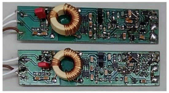
Figure 8.
Two drivers based on the impulse transformer intended for operation in a 2-switch converter.
Table 4.
Main operation parameters of the buck-boost converter laboratory setup.
In terms of immunity of the driver to EMI and common mode issues, the most critical component in the design is the magnetic transformer, which isolates the primary and secondary side galvanically. Some of the parasitic elements in the transformer, but especially the undesired coupling capacitance between the primary and secondary sides, yield an impedance path for coupling currents to enter in the gate loop. Thus, the parasitic impedances must be designed to not affect the operation of the driver. Table 5 shows the main parameters of the transformer of the driver, implemented on a toroid ring core TX16/9.6/6.3 3E5 from FerroxcubeTM, considering the references in Figure 9.
Table 5.
Main parameters of the built transformer.
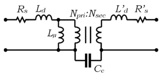
Figure 9.
Equivalent circuit of the transformer.
These parameters have been obtained from three different characterization procedures, at a frequency of 100 kHz. Besides the characteristic short-circuit and open-circuit tests, the primary-to-secondary side capacitance has also been measured. The obtained value for this parameter, close to 3 pF, is in line with the values of the commercial drivers for SiC power MOSFETs [].
5.1. Experimental Characterization of the Working Principle
In order to verify the operating principle of the driver, the main waveforms in key nodes in the driver circuit have been registered. These waveforms can be compared to the theoretical waveforms in Figure 5, but especially with the simulated waveforms shown in Figure 7. Figure 10 shows the waveforms in the driver for an input PWM voltage signal vp(t) of 50% duty ratio and 100 kHz switching frequency, from 0 V to 15 V. The waveform vp(t) is shown in CH1 in Figure 10a, while CH2 and CH3 represent the voltage after derivation in the RC network before, vRC(t), and after, vpri1(t), the BJT power stage, respectively. Figure 10b depicts the signals at the secondary side of the driver. In particular, CH1 and CH3 represent the voltage at the secondary side terminals of the transformer, vsec1(t) and vsec2(t), respectively, measured from the source terminal of the power device. As can be seen by comparing Figure 7 and Figure 10, the simulated waveforms are quite similar to the actual ones, which indicates that the modeling of the circuit has been carried out satisfactorily.
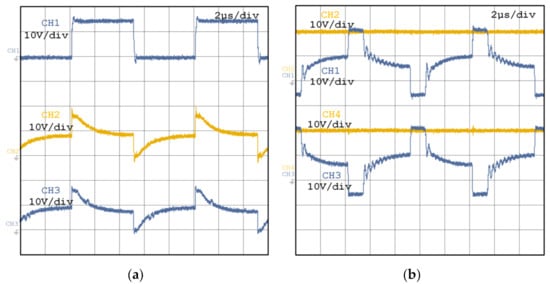
Figure 10.
Main waveforms in the impulse driver (operating principle). (a) CH1: Input PWM signal, vp(t). CH2: derived waveform, vRC(t). CH3: voltage at one primary side terminal, vpri1(t). (b) CH1, CH3: voltage at the secondary side, vsec1(t) and vsec2(t), respectively. CH2, CH4: output voltage supply, vo.
Figure 11 shows additional waveforms to demonstrate the operating principle. CH1 and CH2 in Figure 11a represent the set and reset waveforms, uS(t) and uR(t), respectively, which are the inputs of the flip-flop. These waveforms are generated from the secondary terminals of the transformers by means of the adapting stage shown in Figure 6. CH3 represents the output signal of the OA in the flip-flop, while CH4 depicts the waveform after the output complementary stage, vGS(t). Finally, Figure 11b shows a superposition of the input voltage PWM signal at the primary side of the driver, vp(t), and the output gate-to-source signal, vGS(t) in terminals of the power device, in order to show the synchronization between both signals.
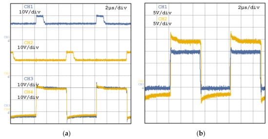
Figure 11.
Main waveforms in the driver based in the impulse transformer to show the operating principle (continued). (a) CH1, CH2: set and reset signals, respectively. CH3: output signal at the flip-flop. CH4: output vGS(t) signal, after the last complementary BJT stage. (b) Superposition of the input PWM waveform, vp(t), and the final output vGS(t) waveform.
Figure 12 shows detailed waveforms of the input and output waveforms in the driver: vp(t) and vGS(t), respectively. In Figure 12a, a detail of the superposed waveforms is shown. Moreover, in Figure 12b, the turn-on and turn-off propagation delays between both waveforms are characterized. It can be seen how the turn-on propagation delay is around 80 ns, while the corresponding turn-off delay reaches 70 ns. However, it must be mentioned that these propagation delays do not depend on the duty ratio, and therefore they can be easily compensated at the control stage in case it is required. This propagation delay is the result of the addition of different propagation delays in the cascaded stages of the driver. Most of the delays in these stages are relatively small, because they come from single analog parts (BJT complementary stages in all solutions, derivative network, etc.). However, the delay imposed by operational amplifier and associated circuitry at the secondary side of the driver cannot be neglected. This delay cannot be actively controlled in the current implementation, but it can be kept below a given design value, provided that the actual part used for the implementation of the OA is selected, taking into account key dynamic parameters from the AC electrical characteristics in the manufacturer’s datasheets.
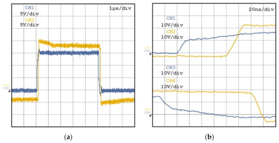
Figure 12.
(a) Detail of the superposition of the input PWM waveform, vp(t) (CH1) and the final output vGS(t) waveform (CH2). (b) Turn-on delay between vp(t) (CH1) and vGS(t) (CH2). Turn-off delay between vp(t) (CH3) and vGS(t) (CH4).
The operation of the driver at several duty ratio values, always at a switching frequency of 100 kHz, can be seen in Figure 13. The operation at duty ratio levels of 20%, 40%, 60% and 80% are shown in Figure 13a–d, respectively. The propagation delay is constant for any duty ratio operation.
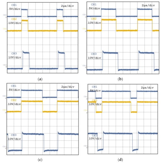
Figure 13.
Operation of the driver at different duty ratio levels. CH1 shows the driving signal from the controller, CH2 shows the signal vp, and CH3 shows the voltage signal at the output of the driver, vGS. (a) d = 20%. (b) d = 40%. (c) d = 60%. (d) d = 80%.
Figure 14 shows the output waveforms when connecting a simple RC network to the G and S terminals of the driver, regarding the rise and fall times at turn-on and turn-off, respectively. It can be seen how the behavior is symmetric for the turn-on and off intervals. It is clear that the turn-on and turn-off delays, as well as the values of the rise and fall times, leave scope for optimization, especially in the selection of components such as the OA or the transistors at the BJT stages. In any case, the functional characterization of the driver has been demonstrated. A representation of the rise and fall times at the output of the driver for all the possible combinations of the R and C values is presented in Figure 15a,b, respectively. The waveforms shown until this point represent the driver operating at a switching frequency of 100 kHz. However, the principle of operation of the impulse transformer is valid for higher switching frequencies, as long as the parts and components are able to function under such conditions. Figure 16a shows the waveforms of the driver operating at 150 kHz, while Figure 16b shows the operation at 200 kHz. Further increase in the frequency was not possible with the laboratory prototype because the losses, specially at the transformer, began to become excessive. In any case, it has been demonstrated how higher frequencies can also be achieved.
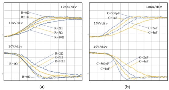
Figure 14.
Rise times (upper traces) and fall times (lower traces) for different RC output load networks in the driver. (a) C = 1nF, R = 0 Ω, 1 Ω, 2 Ω, 5 Ω and 10 Ω. (b) R = 1 Ω, C = 500 pF, 1 nF, 2 nF, 4 nF.
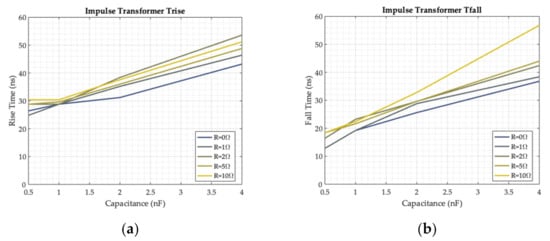
Figure 15.
Rise times (a) and fall times (b) for different RC output combinations in the driver output network (R = [0 Ω, 1 Ω, 2 Ω, 5 Ω], C = [500 pF, 1 nF, 2 nF, 4 nF]).
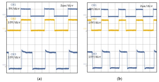
Figure 16.
Operation of the driver at switching frequencies higher than the design value. CH1 shows the driving signal from the controller, CH2 shows the signal vp, and CH3 shows the voltage signal at the output of the driver, vGS. (a) fSW = 150 kHz. (b) fSW = 200 kHz.
5.2. Validation in a Laboratory Converter
Once the working principle had been demonstrated, the next step was to test the operation of the driver in the laboratory prototype shown in Figure 8b, with the ratings given in Table 4. The power DC-DC converter, based on buck-boost topology, is presented in Figure 17. It can be seen how, in this topology the output voltage, Vout presented an inverted polarity. Besides, none of the sources of the power switches were referred to the ground, therefore isolation was required in both drivers. The specific conditions of the operating point in which the waveforms have been registered are described in Table 6. Figure 18 shows the complementary gate-to-source waveforms of the power switches, CH1 and CH2, including a given dead time, generated from a single PWM signal, vp(t) (CH3). Figure 18a,b shows the waveforms for a duty ratio of 50% and 30%, respectively.
Figure 17.
Diagram of the buck-boost converter used for validation of the drivers.
Table 6.
Main operation parameters of the buck-boost converter laboratory setup.
Figure 18.
Complementary gate-to-source waveforms of the power switches, CH1 and CH2, from a single PWM signal, vp(t) (CH3). (a) Duty ratio of 50%. (b) Duty ratio of 30%.
The actual waveforms in the power switches at the converter are shown in Figure 19 for a switching frequency of 100 kHz. The output parameters at the converter were 360 V and 5 A, accounting for an output power of 1.8 kW. The input voltage and current figures were 400 V and 4.7 A, yielding an efficiency of 95% in the converter. The average current in the inductor reached 9.6 A, with a peak-to-peak current value of 4 A.
Figure 19.
Main waveforms in the power stage of the converter operating with the proposed driver. (a) CH1: vGS1(t); CH2: vDS1(t); CH3: vGS2(t); CH4: vDS2(t) (b) Detailed turn-off (up) and turn-on (down) intervals of the waveforms vGS1(t) (CH1, CH3) and vDS1(t) (CH2, CH4).
The rise and fall times of the drain-to-source waveforms are strongly related to the switching power losses. These values in Figure 19b were in the range of 40 ns; they were registered for different vDS levels, and the results can be seen in Figure 20. The values were registered for the C2M0080120D switches with an external gate resistor of 15 Ω, at 100 kHz switching frequency and at 50% duty ratio. The dv/dt value at vDS was, therefore, of around 25 V/ns.
Figure 20.
Rise and fall times in the drain-to-source voltage for different voltage levels.
5.3. Discussion and Conclusions of the Implementation of the Driver Based on the Impulse Transformer
The analysis of results from the design and validation procedure for the driver allow for some conclusions to be made on the performance of the proposed solution. The circuit could operate properly at duty ratio values from 10% to 90%. However, operation beyond 90% is not possible with the current arrangement. This is the greatest limitation of the proposed impulse transformer-based method. Regarding the power consumption of the driver, Figure 21 depicts the power consumption of the driver as a function of the duty ratio and the frequency. Figure 21a shows the consumption at a fixed duty ratio of 50%, for a range of switching frequency from 50 kHz to 220 kHz. On the other hand, Figure 21b shows the power consumption of the driver for 10% to 90% duty ratio, at a fixed frequency of 100 kHz. It must be noted that the power consumption depends largely on the single parts used, such as the OA, the transistors selected for the BJT stages, and so on. Therefore, once the optimization is carried out, a significant reduction in this parameter is expected. This optimization also affects the final size of the driver. It is clear that the largest element is the transformer; therefore, it is the device that limits the power density. The rest of the components in the first driver version are not optimized in size (SMD1206 components, single layer arrangement, etc.). A careful re-design of the driver is expected to reduce the size of the driver by a factor between 3.0 to 4.0.
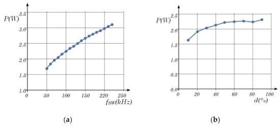
Figure 21.
(a) Driver consumption for different switching frequency values, for a duty ratio of 50%. (b) Driver consumption at 100 kHz for different values of the duty ratio.
The analysis and validation performed for the impulse driver enables the derivation of some general conclusions on the limit values for the switching frequency. The upper switching frequency limit was limited by the power losses in the driver itself. As can be seen in Figure 21a, the relationship between the power consumption and the switching frequency is mainly linear. Thus, a design for higher frequencies needs to carefully consider the constraints imposed by the packaging and system integration, in terms of heat dissipation and thermal behavior. In any case, this analysis needs to be done together with an optimization procedure that jointly considers all these aspects. Regarding the limit for lower frequencies, theoretically any value can be reached, provided that the effective pulse given by the RC time constant and the clamping value discussed previously guarantees that the power required for maintaining the pulse during the duty ratio is supplied to the secondary side. As it was explained before, this condition was met for a minimum duty ratio of 10% for the switching frequency of 100 kHz. However, the lower the switching frequency values, the higher the time constants that guarantee the required power as the frequency decreased, which has implications related to the size of some components in the driver (mainly the transformer and the capacitors at the output stage). Therefore, the implementation of the impulse transformer for low frequencies will penalize the total size of the driver, and therefore the power density of the full system. These constraints in the switching frequency, together with the limitations on the duty ratio, and especially the impossibility of the impulse driver to work at 100% duty ratio operation (complete turn-on of the transformer), limit the applicability of the driver to specific applications. Hence, the next proposal aims to ensure a full range in the duty ratio of the driver.
6. Description of the Modulated Transformer
The second proposal is based on the concept of an HF square waveform that modulates the PWM signal. The modulated signal consists of a waveform that encloses the turn-on and off information of the PWM signal, but with no DC component, thus suitable to be directly connected to the transformer. Besides, the modulating signal can also be used to provide the required power that drives the SiC MOSFET continuously, in a 100% duty ratio condition. This idea was previously explored in ref [], however it is discussed in detail in the following sections. Figure 22 depicts the block diagram that shows this operating philosophy. The starting signal is again the PWM generation block from the digital controller, vp, defined in the same way that in the previous solution. The keystone of the driver is the analog oscillator, osc, that provides an HF square wave signal employed to modulate the input waveform. This oscillator actually provides two output signals, vosc and v′osc, shifted 180°. These signals, shown in the theoretical waveforms presented in Figure 23, independently modulate the input signal, vp, to generate signals vmod and v′mod. In this manner, the differential signal between vmod and v′mod has the shape of vpri depicted in Figure 23. It must be noticed how such a signal has no DC component, and hence it can be directly connected to the primary side of the signal transformer. At the secondary side, the voltage of the signal transformer is rectified to generate signal vrect, thus resembling a waveform that is consistent with the input signal vp in terms of turn-on and turn-off events. This signal, finally, is the input of comparator that allows adapting the voltage values to the ones required for a proper turn-on and off of the SiC MOSFET power switch, vGS. It must be noticed that the output stage is basically the same as in the former case (OA + BJT complementary stage). Moreover, the oscillator osc always remained turned on. This situation opens the possibility of using the signals vosc and v′osc directly to supply a second transformer, which is used to generate the required supply, vo, and reference voltage, vref, at the secondary side of the driver. It can then be assured that the driver operates properly at any duty ratio, including 0% and 100%, thus enabling a full PWM driver scheme. Figure 24 shows a sketch of the theoretical waveforms at the second transformer.
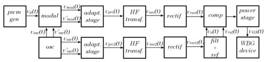
Figure 22.
Block diagram of the driver based on a single impulse transformer.
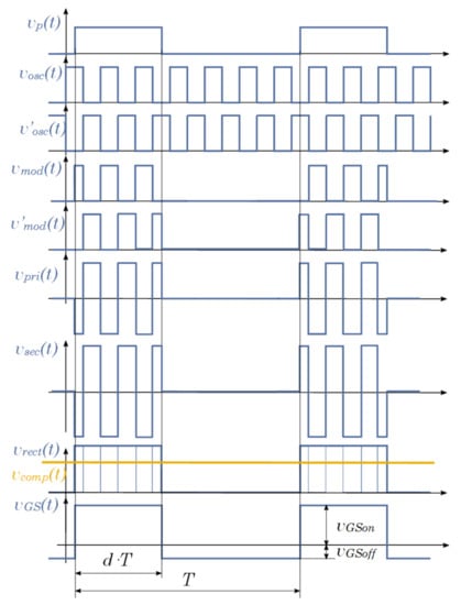
Figure 23.
Theoretical waveforms in the modulated driver.
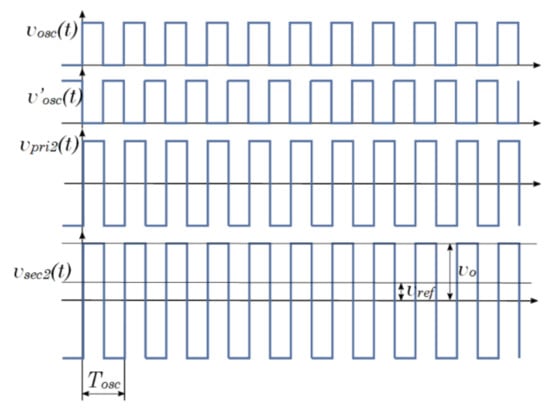
Figure 24.
Theoretical waveforms in the power transformer.
7. Main Characteristics of the Modulated Transformer
As mentioned earlier, the main characteristics of the modulated driver rely on the block that allows the construction of the voltage waveforms at the primary side terminals of the transformer, vmod and v′mod. The selection of the key aspects of the modulation process will define the requirements for the design of the magnetic transformer.
7.1. Implementation of the Working Principle
The working principle of the modulated driver is shown in the diagram of Figure 25. It can be seen how the component count is significantly higher than in the previous solution.
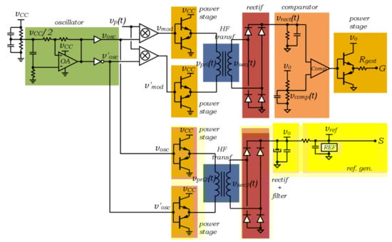
Figure 25.
Detailed diagram of the modulated driver.
7.2. Implementation of the Oscillator and Modulator Stage
The oscillator has been implemented by means of an OA, as depicted in Figure 25. The output of the oscillator is sent to a paired comparator to provide the 180° shifted signals vosc and v′osc. These signals are sent to the analog multipliers, also implemented by means of OA, to provide the signals vmod and v′mod, which have the same sequence of on/off intervals, however have a 180° switch when turned on. Provided that the modulating frequency is significantly higher than the switching frequency, then the signal that is formed by subtracting both vmod and v′mod, vpri presents a null average DC component. These signals, therefore, are connected to the primary terminals of the signal transformer after a BJT complementary stage that provides the required power levels to the signals.
7.3. Characterization of the Transformers
The turns-ratio of the transformer, and the limits for the magnetizing inductance, must be defined in order to design the component. Given that the signal and power transmission are decoupled in this driver, both transformers are defined independently. For the power transformer, the input peak voltage at the primary side is a function of the vCC input power supply voltage, taking into account the voltage drops at the BJT transformer:
The value at the secondary side is given in a similar manner to the former case, and it is given by Equation (5). Therefore, the turns-ratio for the power transformer can be defined as:
The magnetizing inductor of the primary side is designed considering the waveforms involved. Again, the condition in (7) needs to be fulfilled. The same general discussion followed in the former case, from (8)–(10) can be undertaken, but taking into account that the value of the secondary side RMS voltage is known for a square waveform:
The resulting expression for the primary side magnetizing inductor results in:
For the signal transformer, the primary side voltage has the same constraints given in (13), although at the secondary side it has a certain degree of freedom, because the signal is rectified and then compared in an analog comparator to generate the final signal vGS. Therefore, the limits of the voltage after being rectified are given by the output power source values at the secondary side, vo. This value is fixed because the vGSon and vGSoff voltage values for the SiC power MOSFET are known.
Therefore, the turns-ratio for the signal transformer can be defined as:
The magnetizing inductance is also defined as per (16).
7.4. Circuit Modeling and Simulation Results
Table 7 shows the specific part references chosen for the components depicted in Figure 25 for the implementation of the driver circuit.
Table 7.
Commercial parts to implement the driver based on the impulse transformer.
It must be taken into account that the value of the oscillator frequency implemented is:
With these values, the main design constraints for the signal transformer can be calculated:
Additionally, the following expressions are derived for the power transformer:
Figure 26 shows the key simulated waveforms in the driver, for a 40% duty ratio signal with a switching frequency fsw = 100 kHz, and with a modulating frequency fosc = 500 kHz. As can be seen, again the final waveform is generated to reach the values of +20 V/−5 V.
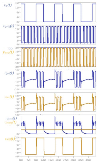
Figure 26.
Main waveforms in the modulated driver (Simulation in LTSpiceTM).
8. Experimental Validation of the Modulated Driver
Following the same methodology developed in the former case, a set of two demonstrators of the modulated driver were designed, built, and tested. Figure 27 shows a photograph of the two demonstrators for this solution. The PCB area of these prototypes was 87 × 21 mm2, similar to the prior solution, although slightly larger. Both the signal and power transformers have been designed following the design constraints defined in Equations (20)–(23), together with the guidelines from the manufacturer. The parts have been built and tested, and their characteristics are shown in Table 8. Again, the references in the equivalent circuit depicted in Figure 9 have been followed.
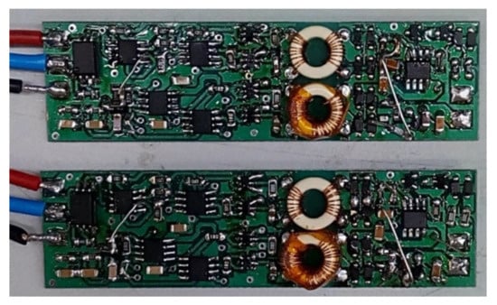
Figure 27.
Two modulated drivers intended for operation in a 2-switch converter.
Table 8.
Main parameters of the built signal transformer.
Experimental Characterization of the Working Principle
The next step was to demonstrate the operating principle of the driver by showing experimental waveforms in key nodes of the driver prototype. The trace CH1 in Figure 28a shows the input waveform of the driver, vp(t), in this case Transistor-Transistor Logic (TTL) levels, from 0 V to 5 V. CH2 shows a first adaptation of the signal from the TTL values to the primary vCC, supply voltage, in this case 15 V. CH3 shows the oscillator voltage, vosc. It can be seen how a slight undesired modulation is present in the frequency of the oscillator, due to non-ideal elements in the OA. In any case, this effect does not affect the operation of the circuit. Traces CH1 and CH2 in Figure 28b show the voltages vmod and v′mod, after the analog modulators. It can be seen that, while turned on, both modulators provided a signal that was 180° shifted. In this manner, the resulting primary side voltage is depicted in CH3.
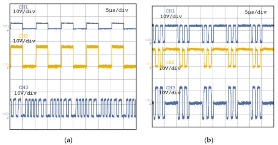
Figure 28.
Main waveforms in the modulated driver to show the operating principle. (a) CH1: input PWM signal, vp(t). CH2: amplified input voltage. CH3: voltage at the output of the analog, vosc(t). (b) CH1, CH2: modulated waveforms with the complementary scheme, to be connected to the primary side terminals of the transformer, vpri1(t) and vpri2(t), respectively. CH3: resulting primary side waveform at the signal transformer, vpri(t).
Figure 29a shows the output of the rectifying stage at the secondary side, after the rectifier formed by the full bridge diode. It can be seen how the information of the turn-on and turn-off intervals are present in this waveform, although the voltage levels are not adequate. This signal was compared with a fixed level, vcomp, by means of the output OA. The output of such amplifier feeds the output BJT complementary stage, in order to amplify the power levels of the output signal, vGS, depicted by CH2 in Figure 29a. The main waveforms at the primary side of the driver, that generate the signals for the power transformer, are shown in Figure 29b. CH1 again shows the amplified input signal. CH2 and CH3 show the signals vosc and v′osc after their respective BJT complementary stages, which are connected to the input terminals of the power transformer. CH2 and CH3 are phase-shifted 180°. CH4 shows the input voltage between the terminals at the primary side of this power transformer; this signal has no DC component. Once the operating principle had been experimentally validated, a series of laboratory tests were carried out in the 2 kW converter with the modulated driver. Trace CH1 and CH2 in Figure 30a show the gate-to-source voltage waveforms at both SiC power switches in the converter, for the operating point defined in Table 6 (400 V/4.7 A input, 360 V/5 A output, 100 kHz). CH3 in turn, shows the drain-to-source voltage waveform at the upper switch in Figure 17, vDS1. Detailed turn-on and turn off MOSFET voltage waveforms are shown in Figure 30b. The values registered were similar to the ones in the previous driver, which was consistent with the fact that the output stage in the driver was very similar in both solutions.
Figure 29.
Main waveforms in the modulated driver to show the operating principle (continued). (a) CH1: rectified waveform at the secondary side of the signal transformer. CH2: final reconstructed waveform after the comparator and BJT stage. (b) CH1: Amplified input voltage. CH2, CH3: vosc and v′osc signals (shifted 180°). CH4: Primary side voltage at the power transformer.
Figure 30.
Operation of the drivers in the laboratory converter. (a) CH1: vGS1(t); CH2: vGS2(t); CH3: vDS1(t). (b) Detailed turn-off (up) and turn-on (down) intervals of the waveforms vGS1(t) (CH1, CH3) and vDS1(t) (CH2, CH4).
The power consumption of the modulated driver has been also characterized, and the main evolution of this parameter is shown in Figure 31. The frequency at the oscillator has been varied from 200 kHz to 600 kHz, maintaining the switching frequency at 100 kHz. Figure 31a shows the trend in the consumption; up to the design level of 500 kHz, the driver operated in a stable manner. For low modulating frequencies (as low as twice the switching frequency) the driver was able to operate adequately, because the square modulating scheme allowed the signal to be reconstructed in the secondary side. However, some undesired glitches, derived from the low modulating frequency appeared in the operation of the driver. These issues, together with possible saturation issues, prevented the use of such low modulating frequencies. On the other hand, for high modulating frequencies (600 kHz and above), even if it is better from the point of view of further size reduction, the power consumption grows dramatically. For the rated modulating frequency of 500 kHz, Figure 31b shows the trend in the power consumption as a function of the duty ratio levels of the input signal vp. It is clear, that, as in the previous case, there is scope for power consumption improvement in the current stage of the driver. Nevertheless, these plots establish the trend of the variation in the power consumption that must guide the optimization procedure. On the other hand, the same remarks about the size optimization, that were established for the impulse driver, can be made for the solution based on the modulating scheme. The size can be largely reduced, although it is true that the component count in this driver is considerably larger than in the impulse case. Still, this driver allows the operation in the full PWM range, i.e., from 0% to 100%.
Figure 31.
(a) Driver consumption for different modulating frequency values, for fSW = 100 kHz and d = 50%. (b) Driver consumption at fSW = 100 kHz and fosc = 500 kHz for different values of the duty ratio.
However, the most important drawback in this design is the need for a second transformer, which has a major issue regarding the CMI, as discussed earlier. This driver has two paths for the undesired induced currents, and besides that, the resulting capacitance is the addition of the individual ones for each of the transformers, resulting in an impedance that is in the order of magnitude of twice the one found for the impulse driver. In order to solve this issue and to implement a solution based on a single transformer, and also to decrease the total component count, a third solution for the implementation of the isolated driver has been explored.
9. Description of the Bilevel Amplitude-Modulated Driver
The third solution can be considered as an evolution of the modulated transformer. In this case, the turn-off state of the input waveform vp does not correspond to a 0 V value in the modulated signal. Instead, the modulated signal is always a square waveform with different amplitudes for turn-on and turn-off, attaining a bilevel AM scheme. The same scheme of the 180° phase shift is employed, to generate an HF signal with no DC component that can be connected to the transformer. Thus, even in the extreme duty ratio conditions of 0% and 100%, the signal can be used for supplying power to the secondary side, and the second transformer is not necessary anymore. This idea was proposed in ref [] for SiC MOSFETS, and in ref [] for GaN power switches. Additionally, a deep analysis of the proposal was carried out in ref []. A block diagram of the driver with bilevel modulation scheme is shown in Figure 32. The solution uses a single transformer, which simultaneously encodes the driving signal and also provides the power requirements for driving the power device. The modulator provides the bilevel scheme, and therefore the resulting signals, vmod and v′mod, presenting the shape that is indicated in Figure 33, where the two different amplitude levels for the turn-on and off intervals can be seen.
Figure 32.
Block diagram of the bilevel amplitude-modulated (AM) driver.
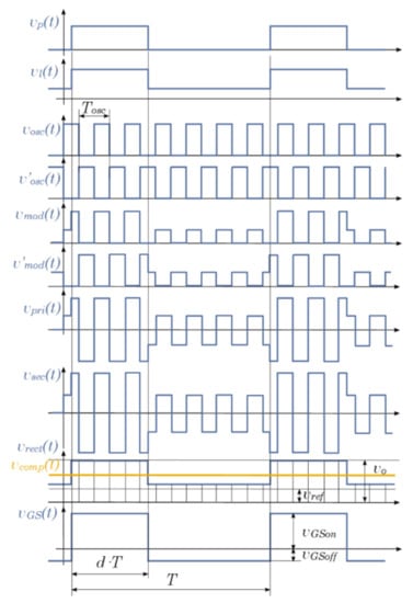
Figure 33.
Theoretical waveforms in the modulated driver.
10. Main Characteristics of the Bilevel AM Driver
The main characteristics of the bilevel AM driver rely on the block that generates the primary side waveforms, vmod and v′mod.
10.1. Implementation of the Working Principle
Figure 34 shows a detailed scheme of the single-transformer circuit that implements the bilevel AM strategy. Both vmod and v′mod modulated signals are amplified by means of two BJT stages, to interface to the primary side terminals of the transformer. The secondary side is now based on a two-winding scheme with a center tap. Therefore, at the secondary side terminals, two rectifiers have been placed, one for generating the signal vrect that is compared to a given value vcomp, at the OA, in order to generate the output waveform vGS. The second rectifier also has a filter in order to supply the output voltage source, vo, to feed the output OA. The reference voltage, vref, required to attain a negative gate-to-source value at turn-off is also connected to this second rectifier. One of the main differences with the former implementation is the inclusion of a synchronization block in the oscillator.
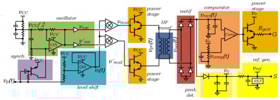
Figure 34.
Detailed diagram of the bilevel AM driver.
10.2. Synchronization Block
Figure 33 shows the most relevant theoretical waveforms in the driver. It can be seen that the oscillator waveform, vosc, and the PWM signal, vp, are not synchronized. This asynchronous feature leads to glitches in the final reconstructed signal in some operating conditions, especially when the duty ratio changes very rapidly, and therefore, a synchronization block has been included to cope with this issue. This block has been represented in Figure 32. The effect of the synchronization block is to reset the oscillator each switching period, in order to provide a much more stable output waveform. The effect of the synchronization block is indicated explicitly in Figure 35.
Figure 35.
Effect of the synchronization in the theoretical waveforms in the bilevel AM driver.
10.3. Characterization of the Transformers
In this case, the turns-ratio and the magnetizing inductor also need to be calculated. However, the constraints already defined for the power transformer in the previous driver are valid in this case, and therefore Equations (5), (13) and (14) define the turns-ratio of the transformer. In addition, for the value of the magnetizing inductor, Equations (15) and (16) can also be used.
10.4. Circuit Modeling and Simulation Results
A complete LTSpiceTM model of the circuit depicted in Figure 34 has been built and simulated. The parts used for the implementation of the driver were the same ones as in Table 7, except for the OA. For this part, an LM6172 was selected, in order to increase the oscillator frequency, fosc, leading to:
With these values, the main design constraints for the signal transformer can be calculated:
Figure 36 shows the main waveforms in a simulation of the bilevel AM driver, for a 45% duty ratio signal, with a switching frequency fsw = 100 kHz, and a modulating frequency fosc = 1 MHz.
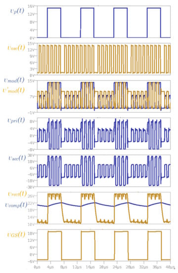
Figure 36.
Main waveforms in the bilevel AM driver (Simulation in LTSpiceTM).
11. Experimental Validation of the Modulated Driver
Figure 37 shows a picture of two bilevel AM drivers, following the procedure already discussed for the previous examples. In the first approach, the resulting size was quite similar to the drivers in the previous two cases. The HF transformer was built following the abovementioned design constraints, and the main parameters are presented in Table 9 (again for the references in Figure 9).
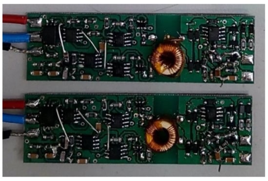
Figure 37.
Two bilevel AM drivers intended for operation in a 2-switch converter.
Table 9.
Main parameters of the built signal transformer.
11.1. Experimental Characterization of the Working Principle
The working principle has been verified experimentally, by acquiring the waveforms in the most significant nodes of the circuit. The input PWM signal was compatible with the common 3.3 V logic levels in digital controllers. CH1 in Figure 38a shows this input voltage signal, vp, from 0 to 3.3 V. CH2 shows the oscillator signal. In Figure 38b, the primary voltage waveforms in the transformer can be seen. CH1 and CH2 show the voltage at the input terminals, vmod and v′mod, and CH3 shows the differential voltage between both input terminals, vpri. CH1 and CH2 in Figure 39a show the voltage at both secondary side terminals, vsec1, and vsec2. In Figure 39b, in turn, CH1 shows the rectified voltage vrect at the input of the comparator used for reconstructing the gate-to-source waveform, while CH2 shows the value of comparison, vcomp. The fit also shows the output of the comparator (CH3), and the reference value vref (CH4). Figure 40a shows the final gate-to-source voltage, vGS (CH2), together with the initial PWM signal, vp. The operation of the two drivers working in a complementary stage with a dead time is shown in Figure 40b. CH1 and CH2 show the input PWM complementary signals at the driver, coming from the digital controller, while CH3 and CH4 show the output vGS signal at the output of the driver. The dead times of 200 ns, and the propagation delay in the drivers can be seen in detail in the waveforms of Figure 41a,b. In the same way as for the impulse transformer, the driver was characterized for a given set of RC loads in the gate and source terminals at the output of the circuit. The representations of the rise and fall times for all the R and C combinations are shown in Figure 42a,b, respectively. Additionally, in order to characterize the operation of the set of two drivers operating in complementary stages for the full PWM range, a series of oscilloscope plots has been registered. Figure 43 shows the operation of the driver inputs and outputs for duty ratios from 10% to 90%. It can be seen how a stable operation can be achieved; the propagation delay is constant for every duty ratio value.
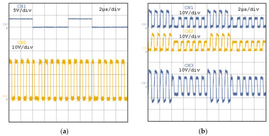
Figure 38.
Main waveforms of the operating principle in the modulated driver. (a) CH1: input PWM signal, vp(t). CH2: voltage at the output of the analog oscillator, vosc(t). (b) CH1, CH2: modulated waveforms with the complementary scheme, to be connected to the primary side terminals of the transformer, vpri1(t) and vpri2(t), respectively. CH3: primary side waveform at the signal transformer, vpri(t).
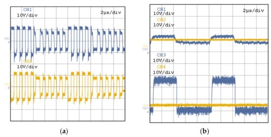
Figure 39.
Main waveforms in the modulated driver to show the operating principle (continued). (a) CH1 and CH2: output voltage at the secondary side terminals of the transformer. (b) CH1: rectified voltage at the secondary side, vrect, at the input of the comparator. CH2: comparison level, vcomp. CH3: output of the comparator (before the BJT amplifying stage). CH4: reference level, vref.
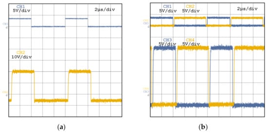
Figure 40.
Main waveforms in the modulated driver to show the operating principle (continued). (a) Input PWM signals, vp1, and output signal, vGS1, for the upper driver (CH1 and CH2, respectively) (b) Input PWM signals, vp1, and output signal, vGS1, for the upper driver (CH1 and CH3, respectively) and vp2 and vGS2 for the lower driver (CH2 and CH4, respectively).
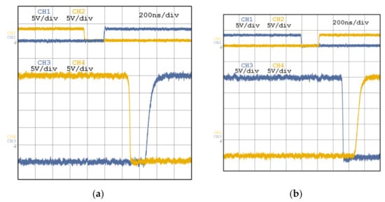
Figure 41.
Input PWM, vp1, and output, vGS1, signal for the upper driver (CH1 and CH3, respectively) and vp2 and vGS2 for the lower driver (CH2 and CH4, respectively). (a) Switch T1 turn-on. (b) Switch T2 turn-off.
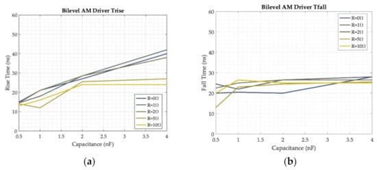
Figure 42.
Rise times (a) and fall times (b) for different RC output combinations in the driver output network (R = [0 Ω, 1 Ω, 2 Ω, 5 Ω], C = [500 pF, 1 nF, 2 nF, 4 nF]).
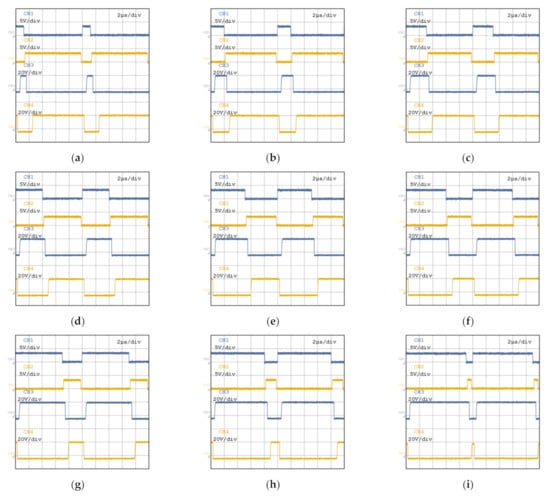
Figure 43.
Input PWM signals, vp1, and output signals, vGS1, for the upper driver (CH1 and CH3, respectively) and vp2 and vGS2 for the lower driver (CH2 and CH4, respectively). (a) d1 = 10%. (b) d1 = 20%. (c) d1 = 30%. (d) d1 = 40%. (e) d1 = 50%. (f) d1 = 60%. (g) d1 = 70%. (h) d1 = 80%. (i) d1 = 90%.
11.2. Validation in a Laboratory Converter
The set of two drivers operating in a complementary scheme has been tested in the laboratory converter and discussed in previous sections of this work. Figure 44 shows the gate-to-source voltage waveforms of the power transistors, vGS1 and vGS2, as well as the drain-to-source voltage waveform, vDS1, at transistor T1 in Figure 17. Detailed sets of waveforms for the turn-on and turn-off intervals of the transistor T1 under the same operating conditions are shown in Figure 45a,b, respectively. It can be seen how some undesired oscillations appear at the gate-to-source voltage waveforms in the exact instant of the power transistor switching. However, these values do not reach the threshold levels that would yield an undesired spurious triggering of the switches, and therefore the system shows adequate noise immunity. This immunity is ensured by a careful design of the PCB layout to minimize the parasitic inductance of the gate loop, but is also possible given the low coupling capacitance CC achieved for the driver.
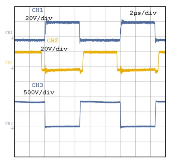
Figure 44.
Operation of the drivers in the laboratory converter. CH1: vGS1(t); CH2: vGS2(t); CH3: vDS1(t).
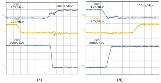
Figure 45.
Operation of the drivers in the laboratory converter. CH1: vGS1(t); CH2: vGS2(t); CH3: vDS1(t) (a) Detailed turn-on interval. (b) Detailed turn-off interval.
Even though the design of the driver has been designed for a switching frequency of 100 kHz, the operation of the circuitry has been validated at higher switching frequencies. Figure 46 shows the laboratory prototype waveforms at the conditions in Table 6, but for switching frequencies of 150 kHz (Figure 46a) and 200 kHz (Figure 46b). Regarding the drain-to-source voltage derivative, similar figures to the ones registered for the previous drivers have been achieved. This is consistent; the output stage was quite similar in all cases. This statement is confirmed by observing the plots in Figure 47, where the rise and fall times in the power switches for the bilevel AM driver are shown.
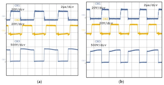
Figure 46.
Operation of the driver at switching frequencies higher than the design value. CH1 shows the driving signal from the controller, CH2 shows the signal vp, and CH3 shows the voltage signal at the output of the driver, vGS. (a) fSW = 150 kHz. (b) fSW = 200 kHz.
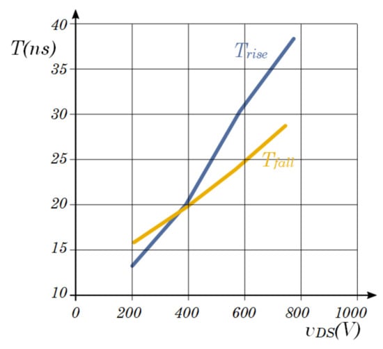
Figure 47.
Rise and fall times in the drain-to-source voltage for different voltage levels.
The last parameter to characterize was the power consumption of the driver. A similar characterization to the one carried out for the former solution was conducted for the bilevel AM driver. The oscillator frequency, fosc, has been varied from 500 kHz up to 1.25 MHz. Figure 48a shows the driver power consumption for that frequency span, at fSW = 100 kHz, for a 50% duty ratio. The consumption is smaller than in the case of the modulated driver with two transformers; however, in an analogous manner, it has been registered that power losses in the driver increase significantly up to dangerous levels for high oscillator frequencies (1.5 MHz and beyond). Lastly, Figure 48b shows the evolution of the power consumption as a function of the duty ratio, for a switching frequency of 100 kHz, an oscillator frequency of 1 MHz, and a duty ratio of 50%.
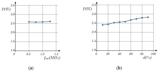
Figure 48.
(a) Driver consumption for different modulating frequency values, for fSW = 100 kHz and d = 50%. (b) Driver consumption at fSW = 100 kHz and fosc = 1 MHz, for different values of the duty ratio.
11.3. Main Conslusions and Discussion on the Bilevel AM Driver
The goal of the research, consisting of a demonstration of the feasibility of the driving scheme based on the bilevel AM strategy, was an isolated driver with full PWM range for SiC power MOSFET switches, which has been successfully attained. It is assumed that, in terms of optimization, significant improvements can be attained in the power consumption and in the size of the bilevel AM driver. Regarding the size, the component count is significantly smaller than in the modulated driver, and therefore the size can be greatly decreased. This decrease in the size is considered one of the main targets in future developments. The rest of the performance, however, in terms of operation, is very similar to that obtained with the former solution, based on the modulation strategy implemented with two transformers.
12. Comparison of Results for the Three Solutions Investigated
This section compares the performance of the three solutions discussed: the first one based on the impulse transformer; the second one based on an on/off modulation scheme implemented with two transformers; and the third one founded on the bilevel AM scheme, implemented with a single transformer. Once the three solutions for the isolated driver were analyzed, built, and tested, a comparison of the performance in power switches was carried out. This comparison focused on the main operational constraints (switching frequency margins, PWM duty ratio limits, switching speed, turn-on and off voltage levels, etc.), as well as electrical features of the driver (CMI constraints, power consumption) or implementation aspects (size, components count, etc.).
12.1. Main Operational Features
The three solutions are able to supply the gating waveforms for SiC power MOSFET switches, with asymmetrical output levels of vGSon = 20 V and vGSoff = −5 V. The target switching frequency was 100 kHz for the demonstrators that have been implemented, but in all cases higher frequencies were attained. The limits of the switching frequency in the case of the impulse-based transformer were solely due the power losses that are a function of this parameter. Therefore, it was easy to reach very high switching frequencies with simple variations of the circuit. Higher switching frequencies have also been achieved in both modulated versions, but in these cases the limitation is imposed not only by the power consumption, but also by the oscillator frequency. Therefore, increasing the switching frequency is also possible, but a careful redesign needs to be carried out in order to ensure that the circuit is able to withstand such conditions. Nevertheless, the distinctive feature of the impulse-based driver vs. the modulated versions is the margins of duty ratio that can be attained. The impulse driver achieves duty ratio margins from 10% to 90%. A 0% operation was also possible, but the 100% operating scheme was not possible with the studied topology. The values of the switching speed, characterized by the derivative of the drain-to-source voltage, vDS, were similar in the three solutions, around 20–25 V/ns. Moreover, these values depend on the output stage, which was the same in the three solutions, therefore independent of the driving approach. This leaves scope for the optimization of this parameter in the case that faster switching speeds are required.
12.2. Additional Electrical Features
In terms of power consumption, the values reported in the study need to be considered carefully; for instance, in the modulated versions, the oscillator frequency was different, which introduced some complexity in the comparison. Although, even if the OAs in the implementations of the three solutions were not the same, it can be concluded that the power consumption of the impulse-based solution was in the same magnitude with the bilevel AM driver, and that the power consumption of the modulator with two transformers was significantly higher than the other two solutions. Regarding the CMI aspects, the best performance was achieved by the bilevel AM driver, which provided the smallest value for the parasitic coupling capacitance between the primary and the secondary side.
12.3. Implementation Aspects
The largest component count was obtained for the modulated driver with two transformers. On the other hand, the lowest component count was attained by the impulse transformer. This parameter is relevant in terms of the achievable size, and also in terms of reliability. However, there is not a clear relationship between component count and final driver size, because the dependency is complex and depends on other factors such as the size of each component, for example. In fact, in terms of size, the three solutions presented had more or less the same size, but it must be noticed that these are not final, commercial drivers, but prototypes intended for the demonstration of the methodologies studied. The main conclusions in this regard are that in all cases the circuits were standard parts, which enabled cheap, reliable, and simple integration of the proposed drivers into the SiC MOSFET module.
13. Conclusions
This work has presented, analyzed, designed, and validated a set of alternate implementations for isolated gate driver circuits for driving power electronics transistors. The proposed topologies for the drivers have been designed specifically for SiC power MOSFETs, however the principles explored are valid for other WBG switches, and in fact one of the solutions has been already assessed for GaN High-Electron-Mobility Transistors (HEMTs). Three different solutions have been analyzed, all of them providing the required gate turn-on and turn-off command signals with the required galvanic isolation, also supplying the required power levels for the secondary side circuitry. In all cases, the isolation was carried out solely by means of magnetic transformers. The resulting solutions, all of them with simple circuitry, enabled the integration of the driver into the power cell, allowing for theoretical higher power density values of the final system. In principle, and considering the former discussion about the component count, the highest power density levels in theory can be achieved by the impulse-based solution, although a thorough optimization procedure needs to be undertaken. Table 10 compares the results of the analyses carried out, and also considers the most usual alternate scheme, that is to say, the implementation of an isolated driver by means of an optocoupler-based signal transfer plus an external isolated DC to DC power source. Some of the parameters can be easily compared. The typical power sources for SiC MOSFET drivers are designed for a power consumption of 2 W in the secondary side of the driver, which is a value in line with the ones presented in the proposed solutions []. Additionally, the value for the coupling capacitance can be easily taken from the datasheets of either these power sources or the optocoupler elements. In this regard, there are a number of reported solutions for isolated gate driving schemes, both commercial parts and research papers, that provide very low coupling capacitances, in the range of 1–3 pF, however these solutions still require an isolated DC-DC power source that will increase the final coupling capacitance level []. Separately, some other references propose implementations for the isolated power supply, with reported coupling capacitance values around 1–3 pF [,,]. However, the solutions discussed in this research would not require any extra component.
Table 10.
Comparative Results.
On the other hand, other functional parameters are very hard to define, given that a manifold of solutions and possible combinations exist in the market. For instance, regarding the switching frequency, if most manufacturers report values up to MHz, it is true that this parameter cannot be compared to the values achieved by the preliminary versions of the demonstrations presented in this work, because an optimization of the implementations is still pending. The same argument is applied to parameters such as the switching speed.
The principle of operation for the three solutions has been discussed, in particular dealing with the use of impulse transformers and square waveform modulation schemes. For each of the solutions, the main relevant implementation details are discussed. A systematic design procedure has been provided for the three driving schemes, including further design details with respect to the reported references [,,,,,]. Finally, the operation of the circuits has been demonstrated experimentally, by testing and characterizing a set of prototypes of these drivers. This provides a comprehensive design example that assesses the feasibility of the proposed solutions.
The main results of the performance of the three gate drivers, on an SiC MOSFET-based prototype, are presented and compared. From this comparison, one of the solutions (the one based in two transformers) can be disregarded, because it has a series of drawbacks that are solved by the bilevel AM scheme. This solution also provides a full PWM range, covering a duty ratio from 0% to 100%, unlike the impulse-based transformer. Future developments of this work include the optimization of the circuit in terms of number of components, part references, size, etc., in order to attain higher power density figures and lower power consumption. Additionally, higher dv/dt and di/dt values at the output of the driver can be attained by optimizing the output stage, formed by the secondary side OA followed by the output complementary BJT stage. In particular, open collector comparators might be used, together with alternate complementary stages.
Another interesting feature is the dynamic variation of the turn-on and off voltage levels vGSon and vGSoff, that might provide better levels of CMI and reliability parameters. Finally, a potential development is the inclusion of current protections and transfer of error signals back to the primary side of the driver, in order to enable fault detection in the driver. Specifically, UnderVoltage-LockOut circuit (UVLO) and desaturation protection (DESAT) must be considered in the industrialization of the proposed solutions. In addition, a key feature to implement is the activation of a fault signal at the primary side of the driver, in order to indicate fault conditions such as the ones indicated (or additional ones such as thermal shutdown), back to the digital controller.
Regarding the application of the proposed solutions to GaN HEMT devices, it must be noticed that the proposed solutions can easily be adapted to this technology. In fact, the on/off modulation scheme has been already applied to such devices, by adapting the final voltage values to reach specific vGSon and vGSoff levels of +6 V and −3 V, respectively []. The same can be applied for the remaining two proposals (the impulse-based driver and the bilevel AM driver), by adapting these values in the design of the transformer and the rest of the circuitry.
Author Contributions
Conceptualization, J.G.; supervision, J.G.; validation, J.G., E.G., A.C. and S.S.; writing—original draft, J.G.; writing—review and editing, J.G., E.G., A.C. and S.S. All authors have read and agreed to the published version of the manuscript.
Funding
This work has been partially supported by the Spanish Government, Innovation Development and Research Office (MEC), under research grant ENE2016-77919, Project “Conciliator”, and research grant PID2019-111051RB-100 Project “B2B-Energy” and by the European Union through ERFD Structural Funds (FEDER). This work has been partially supported by the government of the Principality of Asturias, under Grant FC-GRUPIN-IDI/2018/000241 and under the “Severo Ochoa” program of predoctoral grants for training in research and university teaching, grant number BP16-133.This work has been partially funded by the European Union’s H2020 Research and Innovation program under grant agreement 864459, Project “Cost Effective Technological Developments For Accelerating Energy Transition (TALENT)”.
Data Availability Statement
All the data presented in the study is contained within the article. No new data were created or analyzed in this study apart from the information already shown. Therefore, data sharing is not applicable to this article.
Conflicts of Interest
The authors declare no conflict of interest. The funding sponsors had no role in the design of the study; in the collection, analyses, or interpretation of data; in the writing of the manuscript, or in the decision to publish the results.
References
- Mantooth, H.A.; Glover, M.D.; Shepherd, P. Wide Bandgap Technologies and Their Implications on Miniaturizing Power Electronic Systems. IEEE J. Emerg. Sel. Top. Power Electron. 2014, 2, 374–385. [Google Scholar] [CrossRef]
- Palmour, J.W. Energy Efficient Wide Bandgap Devices. In Proceedings of the 2006 IEEE Compound Semiconductor Integrated Circuit Symposium, San Antonio, TX, USA, 12–15 November 2006; pp. 4–7. [Google Scholar] [CrossRef]
- Musumeci, S. Gate charge control of high-voltage Silicon-Carbide (SiC) MOSFET in power converter applications. In Proceedings of the 2015 International Conference on Clean Electrical Power (ICCEP), Taormina, Italy, 16–18 June 2015; pp. 709–715. [Google Scholar]
- Rice, J.; Mookken, J. SiC MOSFET gate drive design considerations. In Proceedings of the 2015 IEEE International Workshop on Integrated Power Packaging (IWIPP), Chicago, IL, USA, 3–6 May 2015; pp. 24–27. [Google Scholar]
- Kaminski, N. State of the Art and Future of Wide Band-Gap Devices. In Proceedings of the 2009 13th European Conference on Power Electronics and Applications, Barcelona, Spain, 8–10 September 2009. [Google Scholar]
- Lidow, A.; Strydom, J.; de Rooij, M.; Ma, Y. GaN Transistors for Efficient Power Conversion; John Wiley & Sons: Hoboken, NJ, USA, 2012; Chapter 5. [Google Scholar]
- Baliga, B.J. Semiconductors for high-voltage, vertical channel field-effect transistors. J. Appl. Phys. 1982, 53, 1759–1764. [Google Scholar] [CrossRef]
- Lidow, A. Is It the End of the Road for Silicon in Power Conversion? Available online: http://epc-co.com/epc/documents/product-training (accessed on 10 November 2020).
- Buttay, C.; Planson, D.; Allard, B.; Bergogne, D.; Bevilacqua, P.; Joubert, C.; Lazar, M.; Martin, C.; Morel, H.; Tournier, D.; et al. State of the art of high temperature power electronics. Mater. Sci. Eng. B 2011, 176, 283–288. [Google Scholar] [CrossRef]
- Millan, J.; Godignon, P.; Perpina, X.; Perez-Tomas, A.; Rebollo, J. A Survey of Wide Bandgap Power Semiconductor Devices. IEEE Trans. Power Electron. 2014, 29, 2155–2163. [Google Scholar] [CrossRef]
- Lidow, A.; Strydom, J. Gallium Nitride (GaN) Technology Overview; White Paper WP001; European Publishers Council: Bruxelles, Belgium, 2012. [Google Scholar]
- Gaska, R.; Yang, J.W.; Chen, Q.; Khan, A.; Orlov, A.O.; Snider, G.L.; Shur, M.S. Electron transport in AlGaN-GaN heterostructures grown on 6H-SiC substrates. App. Phys. Lett. 1998, 72, 707–709. [Google Scholar] [CrossRef]
- Song, X.; Ni, A.Q.H.X.; Zhang, L. Comparative evaluation of 6kV Si and SiC power devices for medium voltage power electronics applications. In Proceedings of the 2015 IEEE 3rd Workshop on Wide Bandgap Power Devices and Applications (WiPDA), Blacksburg, VA, USA, 2–4 November 2015; pp. 150–155. [Google Scholar]
- Chalker, P.R. Wide band-gap semiconductor: How good is diamond? In Proceedings of the IEEE Colloquium on Diamond in Electronics and Optics, London, UK, 4 November 1993; pp. 1/1–1/3. [Google Scholar]
- Roussel, P. SiC Market and Industry Update; Int. SiC Power Electron. Appl. Workshop: Kista, Sweden, 2011. [Google Scholar]
- Vaculik, P. The properties of SiC in comparison with Si semiconductor devices. In Proceedings of the 2013 International Conference on Applied Electronics (AE), Pilsen, Czech Republic, 10–12 September 2013; pp. 1–4. [Google Scholar]
- Li, X.; Zhang, L.; Guo, S.; Lei, Y.; Huang, A.Q.; Zhang, B.; Xuan, L.; Liqi, Z.; Suxuan, G.; Yang, L.; et al. Understanding switching losses in SiC MOSFET: Toward lossless switching. In Proceedings of the 2015 IEEE 3rd Workshop on Wide Bandgap Power Devices and Applications (WiPDA), Blacksburg, VA, USA, 2–4 November 2015; pp. 257–262. [Google Scholar]
- Hernando, M.; Sebastian, J.; Villegas, P.; Fernandez, A.; García, J.; Rascon, M. Comparing Si and SiC diodes performance in a commercial AC-to-DC rectifier with power factor correction. In Proceedings of the IEEE 34th Annual Conference on Power Electronics Specialist, PESC ’03, Acapulco, Mexico, 15–19 June 2003; Volume 4, pp. 1979–1983. [Google Scholar]
- Bindra, A. Recent Advances in Gate Driver Integrated Circuits for Wide-Bandgap FETs: Manufacturers introduce gate drivers for squeezing the best performance out of WBG devices. IEEE Power Electron. Mag. 2019, 6, 32–38. [Google Scholar] [CrossRef]
- Texas Instruments. IGBT & SiC Gate Driver Fundamentals. Available online: http://ti.com/sic2019 (accessed on 10 January 2021).
- Johnson, M.; Wilson, P.R.; Empringham, L.; Lillo, L.D. IEEE ITRW working group position paper-packaging and integration: Unlocking the full potential of wide-bandgap devices. IEEE Power Electron. Mag. 2018, 5, 26–33. [Google Scholar] [CrossRef]
- Huang, A.Q. Power semiconductor devices for smart grid and renewable energy systems. Proc. IEEE 2017, 105, 1–29. [Google Scholar] [CrossRef]
- Qin, H.; Mo, Y.; Xun, Q.; Zhang, Y.; Dong, Y. A Digital-Controlled SiC-Based Solid State Circuit Breaker with Soft Switch-Off Method for DC Power System. Electronics 2019, 8, 837. [Google Scholar] [CrossRef]
- Wang, Z.; Shi, X.; Xue, Y.; Tolbert, L.M.; Wang, F.; Blalock, B.J. Design and Performance Evaluation of Overcurrent Protection Schemes for Silicon Carbide (SiC) Power MOSFETs. IEEE Trans. Ind. Electron. 2014, 61, 5570–5581. [Google Scholar] [CrossRef]
- Gurpinar, E.; Castellazzi, A. Single-Phase T-Type Inverter Performance Benchmark Using Si IGBTs, SiC MOSFETs and GaN HEMTs. IEEE Trans. Power Electron. 2015, 31, 7148–7160. [Google Scholar] [CrossRef]
- Yin, S.; Wu, Y.; Liu, Y.; Pan, X. Comparative Design of Gate Drivers with Short-Circuit Protection Scheme for SiC MOSFET and Si IGBT. Energies 2019, 12, 4546. [Google Scholar] [CrossRef]
- Sapre, S. Isolated Gate Drivers—What, Why, and How? Available online: https://www.analog.com/en/analog-dialogue/articles/isolated-gate-drivers-what-why-and-how.html (accessed on 11 January 2021).
- Callanan, B. SiC MOSFET Isolated Gate Driver: Cree, Inc. Document Library: Cree, Inc. REV B, 01. 12 2012. Available online: http://www.cree.com/search-results?&search=CPWR-AN10 (accessed on 20 December 2012).
- Chen, H.; Divan, D. High speed switching issues of high power rated silicon-carbide devices and the mitigation methods. In Proceedings of the 2015 IEEE Energy Conversion Congress and Exposition (ECCE), Montreal, QC, Canada, 20–24 September 2015; pp. 2254–2260. [Google Scholar]
- Song, X.; Huang, A.Q.; Lee, M.; Wang, G. A dynamic measurement method for parasitic capacitances of high voltage SiC MOSFETs. In Proceedings of the 2015 IEEE Energy Conversion Congress and Exposition (ECCE), Montreal, QC, Canada, 20–24 September 2015; pp. 935–941. [Google Scholar]
- Tong, C.F.; Nawawi, A.; Liu, Y.; Yin, S.; Tseng, K.J.; Liu, Y.; See, K.Y.; Sakanova, A.; Simanjorang, R.; Gajanayake, C.J.; et al. Challenges in switching waveforms measurement for a high-speed switching module. In Proceedings of the 2015 IEEE Energy Conversion Congress and Exposition (ECCE), Montreal, QC, Canada, 20–24 September 2015; pp. 6175–6179. [Google Scholar]
- Saadeh, O.; Al-Hmoud, A.; Dalala, Z. Characterization Circuit, Gate Driver and Fixture for Wide-Bandgap Power Semiconductor Device Testing. Electronics 2020, 9, 703. [Google Scholar] [CrossRef]
- Li, H.; Munk-Nielsen, S. Detail study of SiC MOSFET switching characteristics. In Proceedings of the 2014 IEEE 5th International Symposium on Power Electronics for Distributed Generation Systems (PEDG), Galway, Ireland, 24–27 June 2014; pp. 1–5. [Google Scholar] [CrossRef]
- Zeng, Z.; Li, X. Comparative Study on Multiple Degrees of Freedom of Gate Drivers for Transient Behavior Regulation of SiC MOSFET. IEEE Trans. Power Electron. 2018, 33, 8754–8763. [Google Scholar] [CrossRef]
- Wang, Z.; Shi, X.; Tolbert, L.M.; Wang, F.; Liang, Z.; Costinett, D.; Blalock, B.J. A High Temperature Silicon Carbide mosfet Power Module With Integrated Silicon-On-Insulator-Based Gate Drive. IEEE Trans. Power Electron. 2015, 30, 1432–1445. [Google Scholar] [CrossRef]
- Wang, P.; Gao, F.; Jing, Y.; Hao, Q.; Li, K.; Zhao, H. An Integrated Gate Driver with Active Delay Control Method for Series Connected SiC MOSFETs. In Proceedings of the 2018 IEEE 19th Workshop on Control and Modeling for Power Electronics (COMPEL), Padova, Italy, 25–25 June 2018; pp. 1–6. [Google Scholar]
- Bhattacharya, S. Wide-band Gap (WBG) WBG devices enabled MV power converters for utility applications 2014; Opportunities and challenges. In Proceedings of the 2014 IEEE Workshop on Wide Bandgap Power Devices and Applications (WiPDA), Knoxville, TN, USA, 13–15 October 2014; pp. 1–125. [Google Scholar]
- Kreutzer, O.; Eckardt, B.; Maerz, M. Optimum gate driver design to reach SiC-MOSFET’s full potential—Speeding up to 200 kV/s. In Proceedings of the 2015 IEEE 3rd Workshop on Wide Bandgap Power Devices and Applications (WiPDA), Blacksburg, VA, USA, 2–4 November 2015; pp. 41–46. [Google Scholar]
- Balcells, J.; Bogónez-Franco, P. Effect of driver to gate coupling circuits on EMI produced by SiC MOSFETS. In Proceedings of the 2013 International Symposium on Electromagnetic Compatibility (EMC EUROPE), Bruges, Belgium, 5–9 August 2013; pp. 209–214. [Google Scholar]
- Balcells, J.; Mon, J.; Lamich, M.; Laguna, A.; Gonzalez, J.M. Improvement of driver to gate coupling circuits for SiC MOSFETS. In Proceedings of the 2014 IEEE 23rd International Symposium on Industrial Electronics (ISIE), Istanbul, Turkey, 1–4 June 2014; pp. 521–525. [Google Scholar]
- Yin, S.; Tseng, K.J.; Tong, C.F.; Simanjorang, R.; Gajanayake, C.J.; Nawawi, A.; Liu, Y.; Liu, Y.; See, K.Y.; Sakanova, A.; et al. Gate driver optimization to mitigate shoot-through in high-speed switching SiC half bridge module. In Proceedings of the 2015 IEEE 11th International Conference on Power Electronics and Drive Systems, Sydney, Australia, 9–12 June 2015; pp. 484–491. [Google Scholar]
- Chen, J.; Li, Y.; Liang, M. A Gate Driver Based on Variable Voltage and Resistance for Suppressing Overcurrent and Overvoltage of SiC MOSFETs. Energies 2019, 12, 1640. [Google Scholar] [CrossRef]
- Chen, J.; Du, X.; Luo, Q.; Zhang, X.; Sun, P.; Zhou, L. A Review of Switching Oscillations of Wide Bandgap Semiconductor Devices. IEEE Trans. Power Electron. 2020, 35, 13182–13199. [Google Scholar] [CrossRef]
- Mermet-Guyennet, M.; Castellazzi, A.; Fabre, J.; Fabre, J.; Ladoux, P. Electrical Analysis and Packaging Solutions for High-Current Fast-Switching SiC Components. In Proceedings of the 2012 7th International Conference on Integrated Power Electronics Systems (CIPS), Nuremberg, Germany, 6–8 March 2012; pp. 1–6. [Google Scholar]
- Collier, L.; Kajiwara, T.; Dickens, J.; Mankowski, J.; Neuber, A.A. Fast SiC Switching Limits for Pulsed Power Applications. IEEE Trans. Plasma Sci. 2019, 47, 5306–5313. [Google Scholar] [CrossRef]
- Qin, H.; Zhao, B.; Xu, W.; Wen, J.; Yan, Y. Evaluation of performance improvement of Silicon Carbide MOSFETs based DC-DC converter. In Proceedings of the 7th International Power Electronics and Motion Control Conference, Harbin, China, 2–5 June 2012; Volume 2, pp. 889–894. [Google Scholar]
- Zhang, Z.; Zhang, W.; Wang, F.; Tolbert, L.M.; Blalock, B.J. Analysis of the switching speed limitation of wide band-gap devices in a phase-leg configuration. In Proceedings of the 2012 IEEE Energy Conversion Congress and Exposition (ECCE), Raleigh, NC, USA, 15–20 September 2012; pp. 3950–3955. [Google Scholar]
- Zhang, Z.; Wang, F.; Tolbert, L.M.; Blalock, B.J.; Costinett, D.J. Active gate driver for fast switching and cross-talk suppression of SiC devices in a phase-leg configuration. In Proceedings of the 2015 IEEE Applied Power Electronics Conference and Exposition (APEC), Manila, Philippines, 18–19 November 2015; pp. 774–781. [Google Scholar]
- Zhang, Z.; Dix, J.; Wang, F.F.; Blalock, B.J.; Costinett, D.; Tolbert, L.M. Intelligent Gate Drive for Fast Switching and Crosstalk Suppression of SiC Devices. IEEE Trans. Power Electron. 2017, 32, 9319–9332. [Google Scholar] [CrossRef]
- Liu, S.; Lin, H.; Wang, T.; Liu, C. Design of Drive Parameters Considering Crosstalk Suppression for SiC MOSFET Applications. In Proceedings of the 2019 IEEE Energy Conversion Congress and Exposition (ECCE), Baltimore, MD, USA, 29 September–3 October 2019; pp. 3281–3286. [Google Scholar]
- Liu, C.; Zhang, Z.; Liu, Y.; Si, Y.; Lei, Q. Smart Self-Driving Multilevel Gate Driver for Fast Switching and Crosstalk Suppression of SiC MOSFETs. IEEE J. Emerg. Sel. Top. Power Electron. 2020, 8, 442–453. [Google Scholar] [CrossRef]
- ACPL-4800 Intelligent Power Module and Gate Drive Interface Optocoupler (277 KB). Available online: http://www.avagotech.com/docs/AV01-0193EN (accessed on 5 May 2016).
- Riazmontazer, H.; Mazumder, S.K. Optically Switched-Drive-Based Unified Independent dv/dt and di/dt Control for Turn-Off Transition of Power MOSFETs. IEEE Trans. Power Electron. 2015, 30, 2338–2349. [Google Scholar] [CrossRef]
- Velander, E.; Kruse, L.; Nee, H.-P. Optimal switching of SiC lateral MOSFETs. In Proceedings of the 2015 17th European Conference on Power Electronics and Applications (EPE’15 ECCE-Europe), Geneva, Switzerland, 8–10 September 2015; pp. 1–10. [Google Scholar]
- Li, C.; Lu, Z.; Chen, Y.; Li, C.; Luo, H.; Li, W.; He, X. High Off-State Impedance Gate Driver of SiC MOSFETs for Crosstalk Voltage Elimination Considering Common-Source Inductance. IEEE Trans. Power Electron. 2019, 35, 2999–3011. [Google Scholar] [CrossRef]
- Gao, F.; Zhou, Q.; Wang, P.; Zhang, C. A Gate Driver of SiC MOSFET for Suppressing the Negative Voltage Spikes in a Bridge Circuit. IEEE Trans. Power Electron. 2018, 33, 2339–2353. [Google Scholar] [CrossRef]
- Wang, G.; Mookken, J.; Rice, J.; Schupbach, M. Dynamic and static behavior of packaged silicon carbide MOSFETs in paralleled applications. In Proceedings of the 2014 IEEE Applied Power Electronics Conference and Exposition—APEC 2014, Beijing, China, 10–12 November 2014; pp. 1478–1483. [Google Scholar]
- Li, H.; Munk-Nielsen, S.; Pham, C.; Beczkowski, S. Circuit mismatch influence on performance of paralleling silicon carbide MOSFETs. In Proceedings of the 2014 16th European Conference on Power Electronics and Applications, Lappeenranta, Finland, 26–28 August 2014; pp. 1–8. [Google Scholar]
- Sadik, D.-P.; Colmenares, J.; Peftitsis, D.; Lim, J.-K.; Rabkowski, J.; Nee, H.-P. Experimental investigations of static and transient current sharing of parallel-connected silicon carbide MOSFETs. In Proceedings of the 2013 15th European Conference on Power Electronics and Applications (EPE), Lille, France, 3–5 September 2013; pp. 1–10. [Google Scholar]
- Chen, Z.; Burgos, R.; Boroyevich, D.; Wang, F.; Leslie, S. Modeling and simulation of 2 kV 50 A SiC MOSFET/JBS power modules. In Proceedings of the 13th European Conference on Power Electronics and Applications, 2009, EPE ’09, Barcelona, Spain, 8–10 September 2009; pp. 1–10. [Google Scholar]
- Wu, X.; Cheng, S.; Xiao, Q.; Sheng, K. A 3600 V/80 A Series--Parallel-Connected Silicon Carbide MOSFETs Module with a Single External Gate Driver. IEEE Trans. Power Electron. 2014, 29, 2296–2306. [Google Scholar] [CrossRef]
- Raszmann, E.; Sun, K.; Burgos, R.; Cvetkovic, I.; Wang, J.; Boroyevich, D. Voltage Balancing of Four Series-Connected SiC MOSFETs under 2 kV Bus Voltage using Active dv/dt Control. In Proceedings of the 2019 IEEE Energy Conversion Congress and Exposition (ECCE), Baltimore, MD, USA, 29 September–3 October 2019; pp. 6666–6672. [Google Scholar]
- Lee, I.; Yue, L.; Yao, X. Voltage Balancing Control with Active Gate Driver for Series Connected SiC MOSFETs. In Proceedings of the 2019 IEEE Energy Conversion Congress and Exposition (ECCE), Baltimore, MD, USA, 29 September–3 October 2019; pp. 3235–3239. [Google Scholar]
- Marzoughi, A.; Burgos, R.; Boroyevich, D. Active Gate-Driver With dv/dt Controller for Dynamic Voltage Balancing in Series-Connected SiC MOSFETs. IEEE Trans. Ind. Electron. 2019, 66, 2488–2498. [Google Scholar] [CrossRef]
- Pawaskar, V.U.; Gohil, G. Closed Loop dv/dt Control for Equal Voltage Sharing between Series Connected SiC MOSFETs. In Proceedings of the 2019 IEEE Energy Conversion Congress and Exposition (ECCE), Baltimore, MD, USA, 29 September–3 October 2019; pp. 3303–3310. [Google Scholar]
- Ericson, N.; Frank, S.; Britton, C.; Marlino, L.; Ryu, S.-H.; Grider, D.; Mantooth, A.; Francis, M.; Lamichhane, R.; Mudholkar, M.; et al. A 4H Silicon Carbide Gate Buffer for Integrated Power Systems. IEEE Trans. Power Electron. 2013, 29, 539–542. [Google Scholar] [CrossRef]
- Valle-Mayorga, J.A.; Rahman, A.; Mantooth, H.A. A SiC NMOS Linear Voltage Regulator for High-Temperature Applications. IEEE Trans. Power Electron. 2013, 29, 2321–2328. [Google Scholar] [CrossRef]
- Yamaguchi, K.; Katsura, K. Research on optimization design of high efficient low noise SiC-MOSFETs inverters. In Proceedings of the 2015 9th International Conference on Power Electronics and ECCE Asia (ICPE-ECCE Asia), Seoul, Korea, 2–4 June 2015; pp. 1442–1448. [Google Scholar]
- Yamaguchi, K.; Sasaki, Y.; Imakubo, T. Low loss and low noise gate driver for SiC-MOSFET with gate boost circuit. In Proceedings of the IECON 2014—40th Annual Conference of the IEEE Industrial Electronics Society, Dallas, TX, USA, 29 October–1 November 2014; pp. 1594–1598. [Google Scholar]
- Yamaguchi, K.; Katsura, K.; Yamada, T.; Sato, Y. Comprehensive study on gate driver for SiC-MOSFETs with gate boost. IEEJ J. Ind. Appl. 2018, 7, 218–228. [Google Scholar] [CrossRef]
- Vrtovec, R.; Trontelj, J. SiC MOSFETs in automotive motor drive applications and integrated driver circuit. In Proceedings of the 2014 29th International Conference on Microelectronics Proceedings—MIEL 2014, Belgrade, Serbia, 12–14 May 2014; pp. 424–430. [Google Scholar]
- Guo, S.; Zhang, L.; Lei, Y.; Li, X.; Xue, F.; Yu, W.; Huang, A.Q. 3.38 Mhz operation of 1.2kV SiC MOSFET with integrated ultra-fast gate drive. In Proceedings of the 2015 IEEE 3rd Workshop on Wide Bandgap Power Devices and Applications (WiPDA), Blacksburg, VA, USA, 2–4 November 2015; pp. 390–395. [Google Scholar]
- Lamichhane, R.R.; Ericsson, N.; Frank, S.; Britton, C.; Marlino, L.; Mantooth, A.; Francis, M.; Shepherd, P.; Glover, M.; Perez, S.; et al. A wide bandgap silicon carbide (SiC) gate driver for high-temperature and high-voltage applications. In Proceedings of the 2014 IEEE 26th International Symposium on Power Semiconductor Devices & IC’s (ISPSD), Waikoloa, HI, USA, 15–19 June 2014; pp. 414–417. [Google Scholar]
- Camacho, A.P.; Sala, V.; Ghorbani, H.; Martinez, J.L.R. A Novel Active Gate Driver for Improving SiC MOSFET Switching Trajectory. IEEE Trans. Ind. Electron. 2017, 64, 9032–9042. [Google Scholar] [CrossRef]
- Acharya, S.; She, X.; Tao, F.; Frangieh, T.; Todorovic, M.H.; Datta, R. Active gate driver for SiC MOSFET based PV inverter with enhanced operating range. In Proceedings of the 2018 IEEE Applied Power Electronics Conference and Exposition (APEC), Port Moresby, Papua New Guinea, 17–18 November 2018; pp. 3230–3237. [Google Scholar] [CrossRef]
- Lee, I.; Yao, X. Active gate control for series connected SiC MOSFETs. In Proceedings of the 2019 IEEE Applied Power Electronics Conference and Exposition (APEC), Anaheim, CA, USA, 17–21 March 2019; pp. 453–457. [Google Scholar] [CrossRef]
- Yang, Y.; Wen, Y.; Gao, Y. A Novel Active Gate Driver for Improving Switching Performance of High-Power SiC MOSFET Modules. IEEE Trans. Power Electron. 2019, 34, 7775–7787. [Google Scholar] [CrossRef]
- Niwa, A.; Imazawa, T.; Kojima, R.; Yamamoto, M.; Sasaya, T.; Isobe, T.; Tadano, H. A dead-time-controlled gate driver us- ing current-sense fet integrated in sic mosfet. IEEE Trans. Power Electron. 2018, 33, 3258–3267. [Google Scholar] [CrossRef]
- Chennu, J.V.P.S.; Maheshwari, R.; Li, H. New resonant gate driver circuit for high-frequency application of silicon carbide mosfets. IEEE Trans. Ind. Electron. 2017, 64, 8277–8287. [Google Scholar] [CrossRef]
- Rothmund, D.; Laboratory, E.Z.P.E.S.; Bortis, D.; Kolar, J.W. Highly Compact Isolated Gate Driver with Ultrafast Overcurrent Protection for 10 kV SiC MOSFETs. CPSS Trans. Power Electron. Appl. 2018, 3, 278–291. [Google Scholar] [CrossRef]
- Zhang, L.; Liu, P.; Huang, A.Q.; Guo, S.; Yu, R. An improved SiC MOSFET-gate driver integrated power module with ultra low stray inductances. In Proceedings of the 2017 IEEE 5th Workshop on Wide Bandgap Power Devices and Applications (WiPDA), Albuquerque, NM, USA, 30 October–1 November 2017; pp. 342–345. [Google Scholar] [CrossRef]
- Peftitsis, D.; Rabkowski, J. Gate and Base Drivers for Silicon Carbide Power Transistors: An Overview. IEEE Trans. Power Electron. 2015, 31, 1. [Google Scholar] [CrossRef]
- Engelmann, G.; Senoner, T.; Doncker, R.W.D. Experimental Investigation on the Transient Switching Behavior of Sic Mosfets Using a Stage-Wise Gate Driver. CPSS Trans. Power Electron. Appl. 2018, 3, 77–87. [Google Scholar] [CrossRef]
- Regardi, M. How Infineon controls and assures the reliability of SiC based power semiconductors. Available online: https://www.ispsd2020.com/exhibitor/document?file=39_1598866100.pdf (accessed on 11 January 2021).
- Kim, T.; Jang, M.; Agelidis, V.G. Ultra-fast MHz range driving circuit for SiC MOSFET using frequency multiplier with eGaN FET. IET Power Electron. 2016, 9, 2085–2094. [Google Scholar] [CrossRef]
- Galai, L.; Costa, F.; Revol, B. EMI disturbance in Double Galvanic Insulation Transformer for high voltage insulation- Application on multilevel converter for 10 kV SiC Mosfet drivers. In Proceedings of the 2012 6th Asia-Pacific Conference on Environmental Electromagnetics (CEEM), Shanghai, China, 6–9 November 2012; pp. 210–213. [Google Scholar]
- Gurpinar, E.; Iannuzzo, F.; Yang, Y.; Castellazzi, A.; Blaabjerg, F. Design of Low-Inductance Switching Power Cell for GaN HEMT Based Inverter. IEEE Trans. Ind. Appl. 2017, 54, 1592–1601. [Google Scholar] [CrossRef]
- Chen, C.; Chen, Y.; Li, Y.; Huang, Z.; Liu, T.; Kang, Y. An sic-based half-bridge module with an improved hybrid packaging method for high power density applications. IEEE Trans. Ind. Electron. 2017, 64, 8980–8991. [Google Scholar] [CrossRef]
- Varajao, D.; Matrisciano, C.M. Isolated Gate Driving Solutions, Increasing Power Density and Robustness with Isolated Gate Driver ICs; Infineon: Neubiberg, Germany, 2020. [Google Scholar]
- Kar, A.; Ahmad, S.S.; Narayanan, G.; Sengupta, M. Design, performance evaluation, fabrication and testing of a SiC MOSFET gate driver. In Proceedings of the 2017 IEEE International Conference on Signal Processing, Informatics, Communication and Energy Systems (SPICES), Kollam, India, 8–10 August 2017; pp. 1–6. [Google Scholar] [CrossRef]
- Zhang, Z.; Wang, F.; Tolbert, L.M.; Blalock, B.J. Active Gate Driver for Crosstalk Suppression of SiC Devices in a Phase-Leg Configuration. IEEE Trans. Power Electron. 2014, 29, 1986–1997. [Google Scholar] [CrossRef]
- Li, Y.; Liang, M.; Chen, J.; Zheng, T.Q.; Guo, H. A Low Gate Turn-OFF Impedance Driver for Suppressing Crosstalk of SiC MOSFET Based on Different Discrete Packages. IEEE J. Emerg. Sel. Top. Power Electron. 2018, 7, 353–365. [Google Scholar] [CrossRef]
- Gill, L.; Ikari, T. Analysis and Mitigation of Common Mode Current in SiC MOSFET Gate Driver Power Supply. In Proceedings of the 2018 IEEE International Conference on Electrical Systems for Aircraft, Railway, Ship Propulsion and Road Vehicles & International Transportation Electrification Conference (ESARS-ITEC), Nottingham, UK, 7–9 November 2018; pp. 1–6. [Google Scholar] [CrossRef]
- Blumenfeld, A.; Cervera, A.; Ben-Yaakov, S. Analysis and design of DC-isolated gate drivers. In Proceedings of the 2012 IEEE 27th Convention of Electrical and Electronics Engineers in Israel, Eilat, Israel, 14–17 November 2012; pp. 1–5. [Google Scholar]
- Zhao, B.; Qin, H.; Nie, X.; Yan, Y. Evaluation of isolated gate driver for SiC MOSFETs. In Proceedings of the 2013 IEEE 8th Conference on Industrial Electronics and Applications (ICIEA), Melbourne, Australia, 19–21 July 2013; pp. 1208–1212. [Google Scholar]
- Ryoo, H.J.; Kim, J.S.; Rim, G.H.; Sytykh, D.; Goussev, G. Current loop gate driver circuit for pulsed power supply based on semiconductor switches. In Proceedings of the 2007 16th IEEE International Pulsed Power Conference, Albuquerque, NM, USA, 17–22 June 2007; Volume 2, pp. 1622–1626. [Google Scholar]
- Wood, P. Transformer-Isolated Hexfet Driver Provides Very Large Duty Cycle Ratios; International Rectifier: El Segundo, CA, USA, 1987. [Google Scholar]
- Zhang, B.; Xie, S.; Xu, J.; Qian, Q.; Zhang, Z.; Xu, K. A Magnetic Coupling Based Gate Driver for Crosstalk Suppression of SiC MOSFETs. IEEE Trans. Ind. Electron. 2017, 64, 9052–9063. [Google Scholar] [CrossRef]
- Hui, S.; Tang, S.; Chung, H.S.-H. Optimal operation of coreless pcb transformer-isolated gate drive circuits with wide switching frequency range. IEEE Trans. Power Electron. 1999, 14, 506–514. [Google Scholar] [CrossRef]
- Bergh, T.; Karlsson, P.; Alakula, M. A resonant galvanically separated power MOSFET/IGBT gate driver. In Proceedings of the 2004 IEEE 35th Annual Power Electronics Specialists Conference (IEEE Cat. No.04CH37551), Aachen, Germany, 20–25 June 2004; Volume 4, pp. 3243–3247. [Google Scholar] [CrossRef]
- Seidel, A.; Costa, M.; Joos, J.; Wicht, B. Isolated 100% PWM gate driver with auxiliary energy and bidirectional FM/AM signal transmission via single transformer. In Proceedings of the 2015 IEEE Applied Power Electronics Conference and Exposition (APEC), Manila, Philippines, 18–19 November 2015; pp. 2581–2584. [Google Scholar]
- Ramesh, C.V.; Krishnan, V.; Ravikumar, H.M.; Manjunatha, A. Design of dual gate driver for IGBT by using pulse transformers without saturation effect. In Proceedings of the 2015 International Conference on Emerging Research in Electronics, Computer Science and Technology (ICERECT), Mandya, India, 17–19 December 2015; pp. 120–125. [Google Scholar]
- Norling, K.; Lindholm, C.; Draxelmayr, D. An Optimized Driver for SiC JFET-Based Switches Enabling Converter Operation with More Than 99% Efficiency. IEEE J. Solid-State Circuits 2012, 47, 3095–3104. [Google Scholar] [CrossRef]
- Pittini, R.; Zhang, Z.; Andersen, M.A.E. Switching performance evaluation of commercial SiC power devices (SiC JFET and SiC MOSFET) in relation to the gate driver complexity. In Proceedings of the 2013 IEEE ECCE Asia Downunder, Melbourne, Australia, 3–6 June 2013; pp. 233–239. [Google Scholar]
- Yu, H.; Lai, J.; Zhao, J.H.; Wright, B.H. Gate driver based soft switching for SiC BJT inverter. In Proceedings of the IEEE 34th Annual Conference on Power Electronics Specialist, PESC ’03, Acapulco, Mexico, 15–19 June 2003; Volume 4, pp. 1857–1862. [Google Scholar]
- Cai, A.; Herreria, A.C.; How, S.B.; Siek, L. 2-Phase 2-stage capacitor-less gate driver for Gallium Nitride Gate Injection Transistor for reduced gate ringing. In Proceedings of the 2015 IEEE 3rd Workshop on Wide Bandgap Power Devices and Applications (WiPDA), Blacksburg, VA, USA, 2–4 November 2015; pp. 129–134. [Google Scholar]
- Weber, S.; Merkert, A.; Mertens, A. Gate driver for safe operation of depletion mode SiC JFETs. In Proceedings of the 2014 IEEE Energy Conversion Congress and Exposition (ECCE), Pittsburgh, PA, USA, 14–18 September 2014; pp. 5716–5722. [Google Scholar]
- Safari, S.; Castellazzi, A.; Wheeler, P. Evaluation of SiC power devices for a high power density matrix converter. In Proceedings of the 2012 IEEE Energy Conversion Congress and Exposition (ECCE), Raleigh, NC, USA, 15–20 September 2012; pp. 3934–3941. [Google Scholar] [CrossRef]
- Riazmontazer, H.; Mazumder, S.K. Dynamic optical turn-off control of a high-voltage SiC MOSFET. In Proceedings of the 2013 Twenty-Eighth Annual IEEE Applied Power Electronics Conference and Exposition (APEC), Bali, Indonesia, 5–7 October 2013; pp. 1274–1278. [Google Scholar]
- Zhang, L.; Guo, S.; Li, X.; Lei, Y.; Yu, W.; Huang, A.Q. Integrated SiC MOSFET module with ultra low parasitic inductance for noise free ultra high speed switching. In Proceedings of the 2015 IEEE 3rd Workshop on Wide Bandgap Power Devices and Applications (WiPDA), Blacksburg, VA, USA, 2–4 November 2015; pp. 224–229. [Google Scholar]
- Chen, Z.; Danilovic, M.; Boroyevich, D.; Shen, Z. Modularized design consideration of a general-purpose, high-speed phase-leg PEBB based on SiC MOSFETs. In Proceedings of the 2011-14th European Conference on Power Electronics and Applications (EPE 2011), Birmingham, UK, 30 August–1 September 2011; pp. 1–10. [Google Scholar]
- Zhang, Z.; Wang, Z.; Wang, F.; Tolbert, L.M.; Blalock, B.J. Reliability-oriented design of gate driver for SiC devices in voltage source converter. In Proceedings of the 2015 IEEE International Workshop on Integrated Power Packaging (IWIPP), Chicago, IL, USA, 3–6 May 2015; pp. 20–23. [Google Scholar]
- Muhsen, H.; Lutz, J.; Hiller, S. Design and Evaluation of Gate Drivers of SiC MOSFET. In Proceedings of the PCIM Europe 2015, International Exhibition and Conference for Power Electronics, Intelligent Motion, Renewable Energy and Energy Management, Nuremberg, Germany, 19–21 May 2015; pp. 1–8. [Google Scholar]
- Lemmon, A.N.; Graves, R. Gate drive development and empirical analysis of 10 kV SiC MOSFET modules. In Proceedings of the 2015 IEEE 3rd Workshop on Wide Bandgap Power Devices and Applications (WiPDA), Blacksburg, VA, USA, 2–4 November 2015; pp. 108–112. [Google Scholar]
- Niwa, A.; Imazawa, T.; Kimura, T.; Sasaya, T.; Isobe, T.; Tadano, H. Novel dead time controlled gate driver using the current sensor of SiC-MOSFET. In Proceedings of the IECON 2015—41st Annual Conference of the IEEE Industrial Electronics Society, Yokohama, Japan, 9–12 November 2015; pp. 001651–001656. [Google Scholar]
- Zhou, Q.; Gao, F.; Jiang, T. A gate driver of SiC MOSFET with passive triggered auxiliary transistor in a phase-leg configuration. In Proceedings of the 2015 IEEE Energy Conversion Congress and Exposition (ECCE), Montreal, QC, Canada, 20–24 September 2015; pp. 7023–7030. [Google Scholar]
- Shen, M. A simple gate assist circuit for SiC devices. In Proceedings of the 2014 IEEE Conference and Expo Transportation Electrification Asia-Pacific (ITEC Asia-Pacific), Beijing, China, 31 August–3 September 2014; pp. 1–6. [Google Scholar]
- Haehre, K.; Simon, C.; Wild, B.; Kling, R.; Heering, W. Design of a 5-MHz-gate-driver for SiC-MOSFETs. In Proceedings of the 7th IET International Conference on Power Electronics, Machines and Drives (PEMD 2014), Manchester, UK, 8–10 April 2014; pp. 1–6. [Google Scholar]
- Whitaker, B.; Cole, Z.; Passmore, B.; Martin, D.; McNutt, T.; Lostetter, A.B.; Ericson, M.N.; Frank, S.S.; Britton, C.L.; Marlino, L.D.; et al. High-temperature SiC power module with integrated SiC gate drivers for future high-density power electronics applications. In Proceedings of the 2014 IEEE Workshop on Wide Bandgap Power Devices and Applications, Knoxville, TN, USA, 13–15 October 2014; pp. 36–40. [Google Scholar]
- De Rooij, M.; Strydom, J.; Van Wyk, J.; Beamer, P. Development of a 1 MHz MOSFET gate-driver for integrated converters. In Proceedings of the Industry Applications Conference, 2002, 37th IAS Annual Meeting, Pittsburgh, PA, USA, 13–18 October 2002; Volume 4, pp. 2622–2629. [Google Scholar] [CrossRef]
- Badawi, N.; Knieling, P.; Dieckerhoff, S. High-speed gate driver design for testing and characterizing WBG power transistors. In Proceedings of the 2012 15th International Power Electronics and Motion Control Conference (EPE/PEMC), Novi Sad, Serbia, 4–6 September 2012; p. LS6d.4-1. [Google Scholar]
- Anthony, P.; McNeill, N.; Holliday, D. High-Speed Resonant Gate Driver with Controlled Peak Gate Voltage for Silicon Carbide MOSFETs. IEEE Trans. Ind. Appl. 2014, 50, 573–583. [Google Scholar] [CrossRef]
- Tang, S.; Hui, S.; Chung, H.S.-H. A low-profile power converter using printed-circuit board (PCB) power transformer shielded with ferrite polymer composite. In Proceedings of the 2000 IEEE 31st Annual Power Electronics Specialists Conference, (Cat. No.00CH37018), Galway, Ireland, 23 June 2000; Volume 3, pp. 1279–1284. [Google Scholar]
- Qi, F.; Xu, L.; Zhao, B.; Zhou, Z. A high temperature de-saturation protection and under voltage lock out circuit for SiC MOSFET. In Proceedings of the 2015 IEEE Energy Conversion Congress and Exposition (ECCE), Montreal, QC, Canada, 20–24 September 2015; pp. 6169–6174. [Google Scholar]
- Qi, F.; Xu, L.; Zhao, B.; Zhou, Z. High current gate drive circuit with high temperature potential for SiC MOSFET module. In Proceedings of the 2015 IEEE Energy Conversion Congress and Exposition (ECCE), Montreal, QC, Canada, 20–24 September 2015; pp. 7031–7037. [Google Scholar]
- Anurag, A.; Acharya, S.; Gohil, G.; Bhattacharya, S. Benchmarking and Qualification of Gate Drivers for Medium Voltage (MV) Operation using 10 kV Silicon Carbide (SiC) MOSFETs. In Proceedings of the 2019 IEEE Applied Power Electronics Conference and Exposition (APEC), Anaheim, CA, USA, 17–21 March 2019; pp. 441–447. [Google Scholar] [CrossRef]
- Berning, D.W.; Duong, T.H.; Ortiz-Rodriguez, J.M.; Rivera-Lopez, A.; Hefner, A.R., Jr. High-Voltage Isolated Gate Drive Circuit for 10 kV, 100 A SiC MOSFET/JBS Power Modules. In Proceedings of the 2008 IEEE Industry Applications Society Annual Meeting, Edmonton, AB, Canada, 5–9 October 2008; pp. 1–7. [Google Scholar] [CrossRef]
- Qi, F.; Xu, L.; Zhao, G.; Wang, J. Transformer isolated gate drive with protection for SiC MOSFET in high temperature application. In Proceedings of the 2014 IEEE Energy Conversion Congress and Exposition (ECCE), Pittsburgh, PA, USA, 14–18 September 2014; pp. 5723–5728. [Google Scholar] [CrossRef]
- Wang, R.; Boroyevich, D.; Ning, P.; Wang, Z.; Wang, F.; Mattavelli, P.; Ngo, K.D.T.; Rajashekara, K. A High-Temperature SiC Three-Phase AC-DC Converter Design for > 100/spl deg/C Ambient Temperature. IEEE Trans. Power Electron. 2013, 28, 555–572. [Google Scholar] [CrossRef]
- Wang, Y.; Krishnamurthy, S. High temperature gate drive circuits for silicon carbide switching devices. In Proceedings of the 2013 IEEE Energy Conversion Congress and Exposition, Denver, CO, USA, 15–19 September 2013; pp. 4258–4262. [Google Scholar]
- Bergogne, D.; Martin, C.; Allard, B.; Falahi, K.E.; Picun, G.; Ezzeddine, H.; Pintout, C. High Temperature Discrete Integrated Coreless Signal Insulator. In Proceedings of the 8th International Conference on Integrated Power Electronics Systems, Nuremberg, Germany, 25–27 February 2014; pp. 1–4. [Google Scholar]
- Nguyen, V.; Le, T.-L.; Sarrafin, F.; To, N.-D.; Colin, D.; Rouger, N.; Lefranc, P.; Lembeye, Y.; Arnould, J.-D.; Allard, B.; et al. Contributions to dedicated gate driver circuitry for very high switching speed high temperature power devices. In Proceedings of the 2016 28th International Symposium on Power Semiconductor Devices and ICs (ISPSD), Prague, Czech Republic, 12–16 June 2016; pp. 443–446. [Google Scholar] [CrossRef]
- Zhang, Z.; Xie, S. A MOSFET’s Driver Applied to High-frequency Switching with Wide Range of Duty Cycles. J. Power Electron. 2015, 15, 1402–1408. [Google Scholar] [CrossRef][Green Version]
- Lu, Z.; Li, C.; Wu, H.; Li, W.; He, X.; Li, S. Design of Active SiC MOSFET Gate Driver for Crosstalk Suppression Considering Impedance Coordination between Gate Loop and Power Loop. In Proceedings of the 2019 IEEE Applied Power Electronics Conference and Exposition (APEC), Anaheim, CA, USA, 17–21 March 2019; pp. 986–990. [Google Scholar] [CrossRef]
- Garcia, J.; Gurpinar, E.; Castellazzi, A. Impulse transformer based secondary-side self-powered gate-driver for wide-range PWM operation of SiC power MOSFETs. In Proceedings of the 2016 IEEE 4th Workshop on Wide Bandgap Power Devices and Applications (WiPDA), Fayetteville, AR, USA, 7–9 November 2016; pp. 59–63. [Google Scholar] [CrossRef]
- Garcia, J.; Gurpinar, E.; Castellazzi, A. High-frequency modulated secondary-side self-powered isolated gate driver for full range PWM operation of SiC power MOSFETs. In Proceedings of the 2017 IEEE Applied Power Electronics Conference and Exposition (APEC), Da Nang, Vietnam, 10–11 November 2017; pp. 919–924. [Google Scholar]
- Garcia, J.; Gurpinar, E.; Castellazzi, A. Full-range PWM isolated gate driver with integrated signal and power transmission to the secondary side of the transformer: A case of study application with SiC MOSFETs. In Proceedings of the ECPE SiC & GaN Forum, Workshop on Potential of Wide Bandgap Semiconductors in Power Electronics Applications, ECPS, Nuremberg, Germany, 8–9 March 2017. [Google Scholar]
- Garcia, J.; Gurpinar, E.; Castellazi, A.; Garcia, P. Self-supplied isolated gate driver for SiC power MOSFETs based on bi-level modulation scheme. In Proceedings of the 2017 IEEE Energy Conversion Congress and Exposition (ECCE), Cincinnati, OH, USA, 1–5 October 2017; pp. 5101–5106. [Google Scholar] [CrossRef]
- Garcia, J.; Saeed, S.; Gurpinar, E.; Castellazzi, A.; Garcia-Fernandez, P. Self-Powering High Frequency Modulated SiC Power MOSFET Isolated Gate Driver. IEEE Trans. Ind. Appl. 2019, 55, 3967–3977. [Google Scholar] [CrossRef]
- Wu, H.; Garcia, J.; Castellazzi, A. GaN HEMT Gate-Driver for Achieving High Power Converter Integration Levels. In Proceedings of the Power Electronics Machines and Drives Conference, PEMD 2018, Liverpool, UK, 17–19 April 2018; IET: London, UK, 2018. [Google Scholar]
- SFDT Design Tool, Ferroxcube. Available online: https://ferroxcube.com/en-global/design_tool/index (accessed on 1 December 2020).
- Murata Power Solutions Inc. NME 5 V–12 V Series Isolated 1W Single Output DC/DC Converters; Murata Power Solutions Inc.: Nagaokakyo, Japan, 2016. [Google Scholar]
- High Isolated DC/DC Converters for Gate Drivers, RECOM. Available online: https://recom-power.com/en/applications/gate-drivers/gate-drivers.html (accessed on 1 December 2020).
- Gottschlich, J.; Schafer, M.; Neubert, M.; De Doncker, R.W. A galvanically isolated gate driver with low coupling capacitance for medium voltage SiC MOSFETs. In Proceedings of the 2016 18th European Conference on Power Electronics and Applications (EPE’16 ECCE Europe), Karlsruhe, Germany, 5–9 September 2016; pp. 1–8. [Google Scholar]
- Srdic, S.; Teng, F.; Lukic, S. High-isolation Low-coupling-capacitance Standalone Gate Drive Power Supply for SiC-based Medium-Voltage Power Electronic Systems. In Proceedings of the 2019 IEEE Energy Conversion Congress and Exposition (ECCE), Baltimore, MD, USA, 29 September–3 October 2019; pp. 3287–3291. [Google Scholar]
Publisher’s Note: MDPI stays neutral with regard to jurisdictional claims in published maps and institutional affiliations. |
© 2021 by the authors. Licensee MDPI, Basel, Switzerland. This article is an open access article distributed under the terms and conditions of the Creative Commons Attribution (CC BY) license (http://creativecommons.org/licenses/by/4.0/).