Article

A Multi-Cache System for On-Chip Memory Optimization in FPGA-Based CNN Accelerators

1
Department of Information Engineering, University of Pisa, Via G. Caruso 16, 56122 Pisa, Italy
2
IngeniArs S.r.l., Via Ponte a Piglieri 8, 56121 Pisa, Italy
*
Author to whom correspondence should be addressed.
Electronics 2021, 10(20), 2514; https://doi.org/10.3390/electronics10202514
Submission received: 7 September 2021 / Revised: 7 October 2021 / Accepted: 12 October 2021 / Published: 15 October 2021
(This article belongs to the Special Issue VLSI Implementation of Neural Networks)

Abstract

:
In recent years, FPGAs have demonstrated remarkable performance and contained power consumption for the on-the-edge inference of Convolutional Neural Networks. One of the main challenges in implementing this class of algorithms on board an FPGA is resource management, especially with regard to memory. This work presents a multi-cache system that allows for noticeably shrinking the required on-chip memory with a negligible variation of timing performance and power consumption. The presented methods have been applied to the CloudScout CNN, which was developed to perform cloud detection directly on board the satellite, thus representing a relevant case study for on the edge applications. The system was validated and characterized on a Xilinx ZCU106 Evaluation Board. The result is a 64.48 % memory saving if compared to an alternative hardware accelerator developed for the same algorithm, with comparable performance in terms of inference time and power consumption. The paper also presents a detailed analysis of the hardware accelerator power consumption, focusing on the impact of data transfer between the accelerator and the external memory. Further investigation shows that the proposed strategies allow the implementation of the accelerator on FPGAs with a smaller size, guaranteeing benefits in terms of power consumption and hardware costs. A broader evaluation about the applicability of the presented methods to other models demonstrates valuable results in terms of memory saving with respect to other works reported in the literature.

1. Introduction

Nowadays, Convolutional Neural Networks (CNNs) are one of the most widespread techniques in image recognition [1,2], audio classification [3,4], and video analysis [5,6]. CNNs have achieved such remarkable results thanks to their extremely high accuracy [7,8], but at the cost of computational power and memory occupation [9,10]. As a consequence, CNN applications are often run on clusters of CPUs or GPUs [11]. These devices are not the best solution whenever the processing of CNN algorithms has to be moved on-the-edge. This expression indicates that computations are performed directly where the information source is, without involving data transfers towards external hardware (e.g., cloud server) for the computations [12]. In recent years, the on-the-edge paradigm has acquired primary importance in many fields such as remote sensing [13], autonomous driving [14], or healthcare [15]. Indeed, it ensures advantages in terms of latency, security, and system-required bandwidth (reducing the amount of raw data to be transmitted) [16]. In this scenario, additional hardware constraints, like the limited power budgets, must be taken into account [17]. Specific devices for the on-the-edge inference of general CNNs have entered the market, such as the Intel Movidius Myriad X VPU [18], the NVIDIA Jetson AGX Xavier [19], the Google Coral [20], and the Gyrfalcon Lightspeeur [21]. FPGAs represent another valid solution as they can provide a good trade-off between performance and power consumption [22,23,24]. In addition, they offer the designer the possibility to develop a custom accelerator for a target network and to integrate onto the same chip dedicated hardware to perform other required tasks such as pre-processing, communication interfaces, or soft-core processors. Moreover, FPGA vendors, such as Xilinx, Microsemi, and NanoXplore, produce radiation hardened devices [25,26,27] that represent a valuable solution for the space market and high-energy physics.
The main challenge in implementing resource hungry algorithms like CNN is to efficiently exploit the resources available in the FPGA. In particular, most recent CNNs [28,29,30] require an amount of memory which often exceeds the storage capability of these devices. For this reason, finding efficient ways to organize data on FPGA resources acquires crucial importance to avoid memory bottleneck in the implementation.
In this paper, we present memory optimization techniques for CNN FPGA-based accelerators. Our goal is to present a design strategy to reduce the overall on-chip memory usage in order to ease the FPGA implementation of CNN models. The presented methods also allow the implementation of a target network on FPGAs with smaller size, thus achieving a reduction of the static power consumption and hardware cost.
The proposed techniques are used to design an accelerator for the CloudScout CNN, a network employed to perform cloud detection on board the CubeSat Phisat-1 [31,32]. The memory footprint of the model amounts to approximately 107 Mbit [13], and it hardly matches the on-chip memory availability of FPGAs. The developed accelerator is then compared with the architecture proposed in [13], which implements the same algorithm covered in this work, in order to have a direct comparison in terms of performance, design portability, and costs.
The main contributions of this work include:
  • design of a cache system that aims at reducing on-chip memory usage by properly re-using input feature maps data and by optimizing on-chip memory footprint for convolutional filters.
  • in hardware implementation and validation of the proposed architectural improvements on a Xilinx ZCU106 Evaluation Board for a case study CNN.
  • characterization of the main system metrics carried on with physical measurements in order to present a benchmark between the developed system and an alternative hardware accelerator for the same CNN reported in the literature [13].
  • detailed analysis on power consumption performed by reporting the current trends of the main system rails during the inference via the Maxim Digital PowerTool Dongle [33].
  • analysis of the enhanced device portability of the design together with the achievable benefits in terms of power consumption and component costs
  • broader evaluation about the applicability of the presented methods to other CNN models and comparison in terms of memory usage with alternative accelerators presented in the literature.
The article outline is the following: Section 2 presents an overview of the state-of-the-art strategies to implement a CNN on board an FPGA with a major focus on memory exploitation. Section 3 describes the proposed memory improvements, while the obtained results are summarized and discussed in Section 4. Finally, Section 5 offers the conclusions of our work.

2. Background

The development of a CNN hardware accelerator on an FPGA is usually a challenging task due to the high degrees of freedom offered by the programmable logic. In the literature, several architectures for realizing such accelerator are described. The proposed strategies deeply vary according to the size of the CNN model and to the available memory budgets. Since the focus of this work is on memory resources, we investigated state-of-the-art methods to address the problem.
The storage of the convolutional filters can be either on-chip or off-chip depending on the model size. In Section 3.2, we will analyze the possible trade-offs of this design choice. There are also different approaches in the storage techniques for the input image and for the hidden layers’ feature maps. The most common methods are the following:
  • fully on-chip: both the input image and the hidden layers feature maps are stored in the FPGA on-chip memories. Such an approach allows for reducing the overheads of off-chip data transfers at the cost of a higher memory occupation. Whenever the CNN memory footprint exceeds the FPGA memory budget, this technique is not viable. The fully on-chip paradigm is the one adopted in [34,35].
  • input image off-chip: a possible strategy to reduce memory usage is to store the input image in an external memory. This solution offers good trade-offs in terms of memory occupation and performance, but it still requires the hidden layers feature maps of the whole CNN to match the FPGA memory availability. Examples of this approach can be found in [36,37].
  • input image and hidden layers feature maps off-chip: this technique stores the input image and the hidden layers feature maps in the external memory. For this reason, it offers the best results in terms of on-chip memory usage. The works presented in [22,23] are based on this method.
Among the illustrated strategies, the ones that move the storage of either the input image or the hidden layers feature maps to the external memory require an on-chip buffer to temporarily save part of the data on board the FPGA [38,39]. Many works in the literature focus on this hybrid storage system, either by optimizing the data transfers with the external memory [40,41] or by presenting solutions to improve the resource management [42,43]. When dealing with these kinds of accelerators, the process in which a smaller quantity of data are extracted from a larger matrix is often called tiling [44]. There are several types of tiling for CNNs since elements can be loaded on-chip in a row-wise, column-wise, or channel-wise order. Different tiling techniques lead to different results in timing performance and memory utilization [45]. Once the tiled data are available in the on-chip buffer, there are multiple possible orders in which they can be read from the memory unit and then delivered to the processing unit. The law that determines this order is also referred to as the scheduling algorithm [46,47]. This algorithm plays a key role in terms of memory usage. Indeed, it determines the number of elements read per clock cycle, P e l e m that linearly affects the memory occupation of the input buffer [13,16,48].
In summary, the absence of an efficient tiling technique and of an efficient scheduling algorithm can easily lead to memory-bounded accelerators by inferring an input buffer that overuses the on-chip memory resources.
This problem was investigated with a theoretical analysis and synthesis results in our previous work [45]. The performed study indicated that the row-wise tiling technique is the best for memory utilization. With regard to the scheduling algorithm, the work identified a valuable way to read the input elements at each clock cycle in terms of memory efficiency. The suggested approach, which coincides with the one adopted in our case study, is reported in Figure 1a. For convenience, from now on, we will refer to the on-chip buffer as the Cache L2 system.
The main idea is to compute an output element by accumulating the convolution intermediate results across the input channels (red arrow) of the feature map and then slide horizontally for the next convolution step (blue arrow). The yellow cube represents the elements extracted from the Cache L2 system at each clock cycle. The parameters I w and I h determine the number of input elements read from a feature map and they are less than or equal to the filter dimensions F w and F h . The parameter I c h is the number of input channels involved in each step. The number of parallelly read data amounts to:
P e l e m = I c h · I w · I h
As shown in Figure 1b, the slide of the convolutional filters is modified whenever a max pool layer is cascaded to the convolutional layer under process. In particular, the generation of the outputs follows the grid order indicated by the subsequent max pooling layer. This technique allows for optimizing performance and power consumption at the cost of increased complexity for the scheduling algorithm.
Notice that, for the sake of clarity, Figure 1 advances the hypothesis that I w × I h coincides with the filter size. In Section 3.1, we will show how to properly modify the scheduling algorithm when this assumption is not true.

3. Methods

The block diagram of the proposed accelerator is reported in Figure 2. The hidden layers’ feature maps and the convolutional filters are stored in the external memory. During the inference, they are progressively loaded in the on-chip caches via an Advanced eXtendible Interface (AXI) bus [49]. The Processing Unit elaborates these data to produce the next layer feature maps, which are then stored back in the external memory.
This section mainly focuses on the implementation of the Cache L1 system and the Filters Cache system. The first is a hardware block capable of providing data re-use for the feature maps elements read from the Cache L2 system. The second is an architectural solution that aims at optimizing the memory utilization for convolutional filters, thus further reducing the accelerator memory footprint.
The microarchitectural design of both units was performed using VHDL for hardware description and QuestaSim for functional validation.

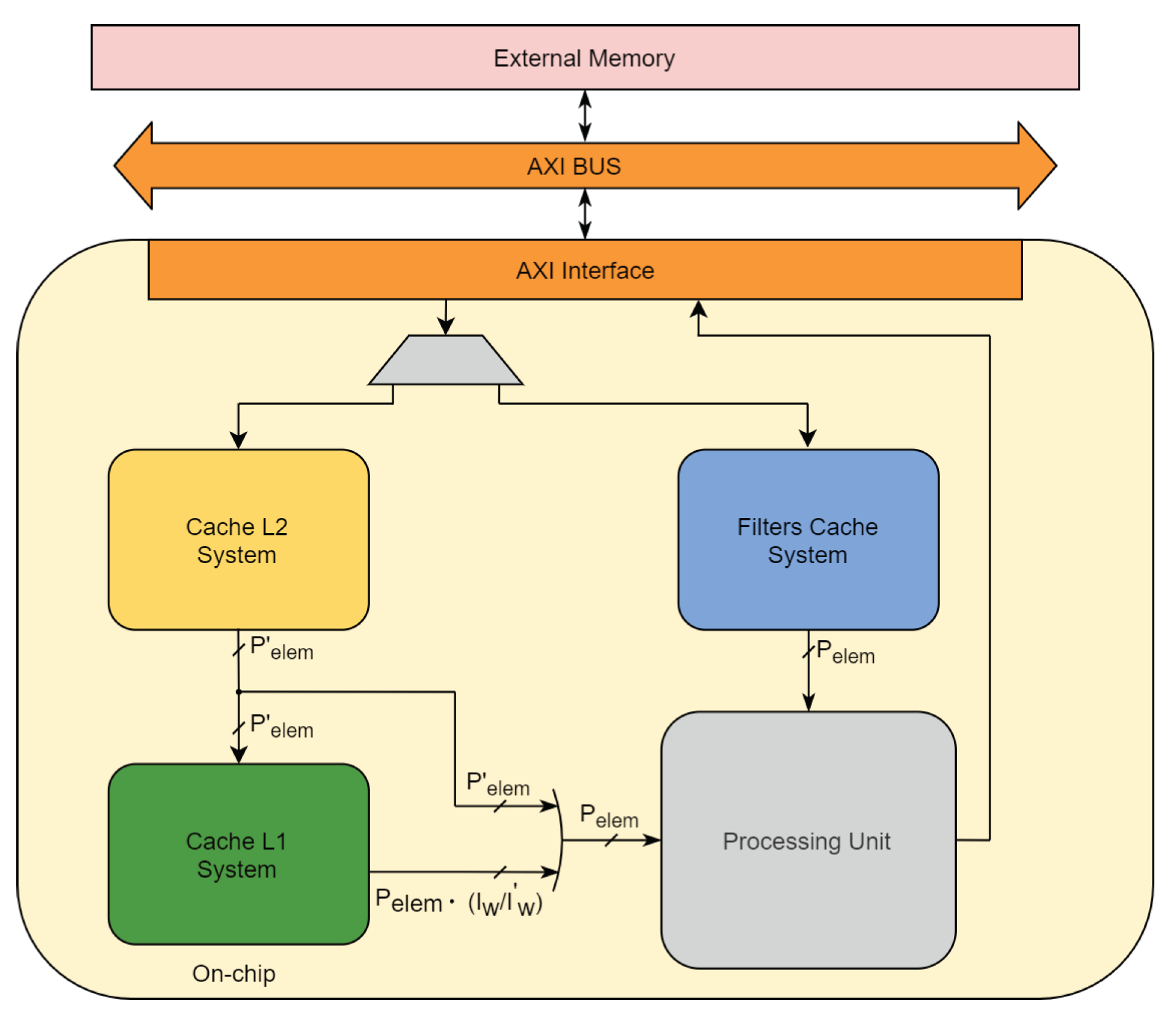
3.1. Cache L1 System

According to the adopted scheduling algorithm, the computations of two subsequent outputs often share a large amount of input feature map elements. This phenomenon does not happen if the horizontal stride S w is greater than or equal to the filter width F w . However, in a large set of convolutional layers, S w is less than F w and the filters partially overlap the adjacent input feature map regions when sliding for the next output computation, as shown in Figure 1. The idea of the Cache L1 system is to buffer the elements already read during the previous convolution step in order to decrease the number of parallelly read data from the Cache L2 system, P e l e m , without significantly affecting the throughput of the accelerator. As previously stated, memory occupation decreases linearly with P e l e m .
The developed Cache L1 system can be composed of one or more sub-modules, units designed to perform data re-use on convolutional layers. The concept behind the Cache L1 sub-module is shown in [45] together with a theoretical study about its applicability and synthesis results. This work presents an implementation strategy to efficiently integrate this sub-module inside a CNN accelerator. In particular, we will show how to modify the scheduling algorithm and how to combine multiple sub-modules to optimize the architecture for models with pooling layers and different kernel sizes.
As a first step, we summarize the functionalities of the Cache L1 sub-module before proceeding with further analysis. This unit performs data-reuse when sliding on a single row of the input feature map for a fixed layer. In particular, the aim of the Cache L1 sub-module is to decrease P e l e m by appropriately reducing I w , i.e., the number of kernel columns read. The value of I w after the introduction of the Cache L1 sub-module will be referred to as I w .
The operating principle of the Cache L1 sub-module is presented in Figure 3 by considering a layer with filter size f = 3 × 3 and horizontal stride S w = 1 . In this example, we will assume to decrease P e l e m by passing from I w = 3 to I w = 1 .
The yellow box, which represents the elements read from the Cache L2 at each clock cycle, is characterized by I c h = 1 , I h = 3 and I w = 1 .
At the beginning of each row, the input data are read from the Cache L2 following the column-wise order reported in Figure 3a. The numbers indicate the position of the yellow box at consecutive clock cycles. At this stage, the Cache L1 sub-module is loaded for the first time and does not output any data. Once the first output is computed and the filter shifts from this position, the Cache L1 sub-module starts providing part of the required elements (green blocks in Figure 3b).
In the regime condition, the Cache L2 only provides elements belonging to the same column, while the other two columns are read from the Cache L1 sub-module. The process described in Figure 3b continues until the last elements of the row have been processed. At this point, the sub-module returns to the idle state after flushing the stored data, and it is ready to process a new row.
It must be noticed that our VHDL custom design includes all the necessary hardware blocks for the address management. The read/write operations between the external memory and the Cache L2, and between the Cache L2 and the Cache L1 are all deterministic, following the order defined by the chosen scheduling algorithm. The miss condition for the proposed Cache system coincides with the lack of sufficient data for proceeding with a convolution step. This event happens when the Processing Unit (please refer to Figure 2) elaborates data faster than the AXI Bus sending data to the Cache L2. Indeed, the probability of a miss condition depends on the computational power of the Processing Unit and on the speed and arbitration of the AXI Bus. If a miss condition occurs, appropriate control logic freezes the Processing Unit until sufficient data are available in the Cache L2.
In the example reported in Figure 3, the Cache L1 sub-module works under the hypothesis of storing one column per clock cycle, i.e., I h = F h . However, in cases such as filters with size f = 5 × 5 or f = 7 × 7 , this assumption may lead to excessive memory usage since P e l e m linearly depends on I h . For this reason, in this work, we upgraded the scheduling algorithm in order to include the possibility to slide the yellow box across the column if necessary. If F h is not a multiple of I h , the Cache L2 provides I h elements whenever possible and ( F h mod I h ) at the end of the column. Figure 4 reports an example of this scheduling strategy for a layer with f = 5 × 5 , S w = 1 and I h = 3 . As it can be noticed, for each column, the Cache L2 firstly provides the upper three elements and then the remaining two. Once the value of I h is fixed, the same operating principle is applied to filters with different size f [ 7 × 7 , 11 × 11 , ] . In order to deliver to the Cache L1, the data generated according to this scheduling algorithm, we designed a control circuit that takes as input a maximum of I h elements ( I h < F h ) per clock cycle and provides F h elements to the Cache L1 sub-module when ready. In this way, the Cache L1 sub-module receives F h elements at a time and the designer is free to size I h according to the memory requirements of the application.
If I c h > 1, each input channel is executed in parallel with the others following the scheduling operations described above.
For what has been discussed so far, the new number of parallelly read elements from the Cache L2 can be computed as in Equation (2):
P e l e m = I c h · I w · I h
The depth, the word width, and the memory footprint of the Cache L1 sub-module for a specific layer are given by:
D s u b = C h i n
W s u b = ( F w I w ) · F h · b i n
M s u b = D s u b · W s u b = C h i n · ( F w I w ) · F h · b i n
where C h i n is the number of input feature maps of the layer, and b i n corresponds to the representation bits of the input elements. In terms of timing performance, the system slows down by a factor of P e l e m / P e l e m at the start of each row only. Indeed, in this step, the Cache L1 is empty and the Cache L2 needs more time to provide all the required elements due to the lower number of outputs. The timing slowdown for a given layer can be computed as indicated in (6):
T s d = I F M h · C h i n · F w · F h P e l e m C h i n · F w · F h P e l e m · T c l k
where I F M h is the input feature map height, and T c l k is the clock period of the accelerator.
In the following, we will discuss how the Cache L1 sub-module can be employed in a complete hardware implementation of a CNN model. The Cache L1 System combines multiple Cache L1 sub-modules to achieve an implementable design for a CNN characterized by several layers with different filter sizes and with max pooling operations. More precisely, layers with the same filter size exploit the same sub-module. The shared sub-module must be sized in order to be able to process the worst case among the selected layers, i.e., the layer with the highest number of elements to be cached. The sub-module memory footprint for a fixed filter size f = F w × F h can be calculated as:
M s u b f = ( F w I w ) · F h · max q L f { C h i n q } · b i n
where q is the layer index and L f is the set of layers with filter size f on which data re-use can be applied. In addition, multiple sub-modules must be inferred by the synthesis tool for those convolutional layers followed by max pooling layers. Indeed, the scheduling algorithm described in Section 2 simultaneously computes several output rows whenever max pool is applied. If the max pooling operations are performed on a P q · P q grid, then the number of parallelly computed rows is equal to P q . This is also the number of sub-modules to be inferred since each block can process a single row of outputs at a time. From this analysis, we can deduce that the number of sub-modules to be inferred for a given filter size f can be expressed as:
N s u b f = max q I ( P q )
According to this, the total memory footprint of the Cache L1 system is computed as:
M s y s = f M s u b f · N s u b f
Figure 5 reports the Cache L1 system architecture with further details on the additional logic responsible for the selection of the correct sub-module while performing computations on a generic layer.

3.2. Filters Cache System

A possible approach in the design of CNN accelerators is to fit the whole set of convolutional filters directly in the FPGA resources [50,51,52]. Such a design choice benefits the system in terms of timing performance as it avoids the off-chip data transfers required by external memories. Nevertheless, this approach prevents the optimal exploitation of memory resources since the computation of a layer requires the on-chip availability of only a subset of the total filters collection. In addition, the on-chip storage of the entire filter set can be unfeasible when the complexity of the network grows [28,29,30]. For this reason, we designed the Filters Cache system, a memory unit that allows storing on-chip the filters of the layer under process while the rest is saved in an external memory. Once the computation of a layer ends, the stored filters are updated to proceed with the processing of the subsequent layer. The depth, the word width, and the memory footprint of the block are given by:
D w = max q L { C h i n q }
W w = max q L { F w q · F h q · b f i l t e r q }
M w = D w · W w = max q L { C h i n q · F w q · F h q · b f i l t e r q }
where L is the layers collection and b f i l t e r corresponds to the filters representation bits.
In the fully on-chip approach, the required memory footprint is higher since it is computed by replacing the max value with the sum of all contributions. The additional time necessary to update the Filters Cache for the whole network can be estimated as:
T w = q L F w q · F h q · C h i n q · b f i l t e r q b w i d t h · T c l k
where b w i d t h is the width of the communication bus with the external memory.

4. Results

The presented architectural improvements were implemented for the CloudScout CNN presented in [32]. The network processes 512 × 512 × 3 images through ten convolutional layers and two fully connected layers. The first layer is characterized by a 5 × 5 filter with a 2 × 2 max-pooling. It is then followed by three triplets of convolutional layers: each triplet exploits a sequence of filters of 3 × 3 , 1 × 1 , 3 × 3 , and finally applies 2 × 2 max pooling [32]. All convolutional layers have horizontal stride S w = 1 . The developed Cache L1 system was equipped with four sub-modules, two for the 5 × 5 layer and two for the 3 × 3 layers, to match the network parameters. No sub-modules were inferred for the 1 × 1 layers as they do not exploit data re-use. Table 1 provides an overview on the parameters useful for the design of the Cache L2 system.
The first row of Table 1 reports the set of parameters that directly depend on the model features while the second row shows the ones chosen for the architecture development. The values of I c h , I h , and I w were sized to achieve a valuable trade-off between power consumption and inference time. The Cache L1 system allows for reducing the memory usage by passing from ( I w , P e l e m ) to ( I w , P e l e m ) without significantly affecting the metrics mentioned above, as we will show in this section.
Please notice that, despite the presence of a layer with f = 5 × 5 , we chose I h = 3 by considering only the memory requirements thanks to the improved scheduling strategy illustrated in Section Figure 5.
The design was implemented on a Xilinx ZCU106 Evaluation Board featuring a Zynq Ultrscale+ ZCU7EV FPGA in order to benchmark the accelerator with the one described in our previous work [13]. The implementation results of the developed system are reported in Table 2 together with the one of the hardware accelerator proposed in [13]. The architectures are referred to as respectively the Memory-optimized Accelerator and the Base Accelerator.
The Cache L2 system is the block responsible for the URAM resources utilization. In the upgraded accelerator, the number of URAMs decreases from 54 to 18, as expected by choosing P e l e m / P e l e m = 3 . This allows for reducing the Cache L2 block memory footprint from 15.19 Mbit to 5.06 Mbit. The Cache L1 system requires 3 BRAM units and 368 LUTRAMs for a total memory footprint of 0.105 Mbit, which is coherent with the results provided by Equation (9). In particular, the 5 × 5 sub-modules employ two 320 × 3 memories that are not efficiently mapped on BRAM units (9 BRAMs required) despite their negligible size. For this reason, we implemented these sub-modules in LUTRAMs to further optimize the design. Conversely, the 3 × 3 sub-modules are based on BRAM blocks. The remaining BRAM resources are exploited for the AXI communication FIFOs (4 BRAM required) and for the on-chip storage of convolutional filters. The introduction of the Filters Cache system allows for halving the memory utilization for this task by passing from 64 to 32 units, thus saving 1.13 Mbit.
The overall memory utilization of the system is 6.43 Mbit, which is clearly an improvement when compared to the 17.58 Mbit of the starting accelerator. The frequency of the AXI interface f a x i and the frequency of the accelerator f a c c are unchanged since the proposed architecture does not affect the critical path timing.
The system was validated and characterized within the testing environment presented in [13]. We performed the inference time measure by using an internal counter triggered at the start of the inference and read at the end by the ARM Cortex a53 hardcore processor. With regard to power measures, we applied the methods described in [53,54] while processing multiple inferences. In particular, data were collected through the INA226 power monitors hosted on the ZCU106 for the various power rails via software and were compared with current measures logged via the Digital PowerTool software from Maxim Integrated [33]. Power measurements were repeated also for the base accelerator in order to take into account the VDDQ power supply rail of the off-chip MT40A256M16GE-075E DDR4 memory [55] (rail not considered in [13]).
Table 3 reports the power consumption P c , the inference time T i n f , the energy per inference E i n f , and the classification accuracy A c c . In order to offer a term of comparison with an embedded CNN accelerator, we also reported these metrics for the Intel Movidius Myriad 2 implementation [18].
The Memory Optimized Accelerator achieves better inference times at the cost of a higher power consumption when compared to the VPU solution. The negligible accuracy drop is caused by the quantization process performed on the model before the FPGA implementation.
When compared to the Base Accelerator, we notice that the power consumption P c has increased by 0.12 W. The voltages of the monitored rails together with the measured currents are listed in Table 4 [54,56].
Figure 6 reports the current trends extracted directly from the Digital PowerTool interface. The value of P c is obtained as the sum of all power contributions.
The main contribution to the power increase is given by the higher number of inferred LUTs and registers.
The reduction of the URAM and BRAM memories does not significantly diminish power consumption as suggested by the Vivado Power Estimator. Indeed, the tool indicates that each of these resources is responsible for 2% of the total power consumption.
The off-chip storage of the filters negligibly affects power consumption. The power variation obtained by monitoring the VDDQ power supply rail [55] via the Digital PowerTool amounts to 0.012 W. The trends of the currents belonging to this rail are reported in Figure 7 for both the accelerators. This result is reasonable when considering that the off-chip storage of the filters increases the number of reading and writing operations in the external memory as well as the processing time.
The inference time T i n f is now 3.1 ms longer, which is caused by the slowdown introduced by the Cache systems as described in Section 3.1 and Section 3.2.
The energy per inference E i n f is 0.3 W higher because it is the product of P c and T i n f . The data transfers of the filters do not significantly affect the energy consumption since the filters’ memory footprint amounts to 2.2 Mbit, which constitutes only 2% of the overall transferred data during an inference.
As shown in Table 3, the accuracy is the same for both accelerators. In fact, the applied architectural improvements do not modify the functional behavior of the system, thus leaving this metric unchanged.
We implemented the system on different FPGAs to prove the enhanced portability of the developed accelerator. The selected devices are the following:
  • Xilinx Zynq Ultrascale+ ZU3EG;
  • Xilinx Zynq 7000 Z7030;
  • Xilinx Kyntex Ultrascale KU025;
  • Xilinx Artix 7 XC7A200T;
  • Intel Arria 10 GX 270.
These components were chosen from different FPGA families in order to extend the results of our analysis on a heterogeneous set of devices. Figure 8 reports the on-chip memory budgets of the target FPGAs together with the one of the ZU7EV, which is the FPGA hosted on the ZCU106 Evaluation Board.
The red dashed lines represent the memory footprints required by the two accelerators under analysis. As the figure suggests, the implementation of the system without the proposed memory improvements is not feasible on the new set of devices due to the reduced memory availability.
Moreover, FPGAs with smaller area usually come also with a lower number of DSP units, which are heavily exploited resources by CNNs. In order to match the DSP availability of the proposed devices, we reduced the number of Multiply and Accumulate (MAC) blocks instantiated in the Processing Unit. These units are responsible for the computational operations required by convolutions and they are the main source of DSP usage. More specifically, we halved the number of MAC blocks, thus passing from 576 to 288 Xilinx DSP slices used by the Processing Unit. This change causes an increase of the inference time T i n f by a 2 x factor since this metric linearly depends on the Processing Unit throughput. On the other hand, the classification accuracy A c c is unchanged since the number of MAC blocks does not affect the results of the inference.
Table 5 reports the implementation results on the considered FPGAs.
The RAM Blocks indicate, respectively, BRAM units or M20K blocks whether the FPGA is a Xilinx or Intel product. The absence of URAM memories within these devices was compensated by using RAM blocks in their place. The DSP usage varies from Xilinx to Intel FPGAs since the considered devices exploit different hardware primitives for these resources. We chose the same clock frequency (constrained by the least performing device) in order to perform a power comparison. Figure 9 reports the static and dynamic power estimated for the same design at the fixed clock frequency with the Vivado Power Analyzer and the Quartus Power Analyzer, respectively, for Xilinx and Intel FPGAs. The lowest power consumption amounts to 0.64 W, which is 63.34% inferior to the one achievable with the ZCU106 Evaluation Board (ZU7EV FPGA). Even if this analysis is just an estimation of the real power consumption, it suggests that the application of the proposed architectural strategies on a target design allows for reducing the power consumption by migrating on FPGAs with smaller size. In addition to this, a benefit of this enhanced portability is also the reduction of the device cost. We included the Arria 10 GX 270 in our analysis because, despite higher power consumption, it provides a characterization of our accelerator also in terms of Intel FPGA resources.
Finally, Table 6 reports an estimate of the on-chip memory requirements of the designed system for commonly used CNNs: LeNet-5 for MNIST, NiN for CIFAR10, and VGG-16 for ImageNet. The aim of this analysis is to show how the proposed memory optimizations scale on different models while tuning the architecture parameters, and to present a first comparison in terms of memory usage with alternative accelerators presented in the literature. The implementation and characterization of the reported configurations, together with a detailed comparison in terms of performance with the other accelerators, require a more careful analysis which will be part of our future work.
From Table 6, we observe that, as mentioned in Section 3.2, the Filters Cache plays a key role when moving to larger models such as VGG-16. Indeed, for this network, the number of convolutional filters far exceeds the memory budget of many FPGA devices and the introduction of the Filters Cache allows for solving this problem.

5. Conclusions

This article presents the Cache L1 system and the Filters Cache system, two memory optimization techniques for CNN hardware accelerators.
The Cache L1 system is an architectural unit designed to implement data re-use on the input feature maps’ elements. The provided analysis shows that this block allows for reducing the overall memory resources by decreasing the size of the input feature maps buffer, i.e., the Cache L2 system.
The Filters Cache system allows for optimizing the required on-chip memory for convolutional filters by limiting the storage to the filters of a single layer at a time.
The proposed architectural improvements were exploited to design an accelerator for the CloudScout CNN proposed in [32]. The system was validated and tested on the Xilinx ZCU106 Evaluation Board. The result is a memory reduction of 63.48%, passing from 17.58 Mbit to 6.42 Mbit, when compared to an alternative hardware accelerator for the same CNN proposed in [13]. The Cache L1 system and the Filters Cache system allow for saving, respectively, 58.19% and 5.29% of the total memory resources. The variations in the inference time and in the power consumption, which amount to 2.14 % and 2.73 % , prove that the memory optimization slightly affects the accelerator performance.
Further investigation demonstrates that the memory-optimized system has higher portability in terms of device choice thanks to the enhanced efficiency in resource exploitation. Several implementations of the presented accelerator on devices with smaller size are reported in order to prove this achievement. The migration of the accelerator on these FPGAs allows for reducing power consumption and device cost.
Finally, a preliminary analysis about the applicability of our methods to other CNN models shows valuable results in terms of memory saving even in comparison with other works from the literature.

Author Contributions

Conceptualization, G.D.; methodology, T.P. and E.R.; software, T.P. and E.R.; validation, T.P.; formal analysis, T.P. and G.D.; investigation, T.P. and E.R.; resources, L.F.; data curation, T.P. and E.R.; writing—original draft preparation, T.P.; writing—review and editing, G.D. and E.R.; visualization, T.P.; supervision, L.F.; project administration, L.F.; funding acquisition, L.F. All authors have read and agreed to the published version of the manuscript.

Funding

This work has been partially funded by the European Space Agency under contract number 4000129792/20/NL and by the European Union’s Horizon 2020 innovation action under Grant No. 761349, TETRAMAX (Technology Transfer via Multinational Application Experiments).

Conflicts of Interest

The authors declare no conflict of interest.

Abbreviations

The following abbreviations are used in this manuscript:
AXIAdvanced eXtendible Interface
BRAMBlock RAM
CNNConvolutional Neural Network
CPUCentral Processing Unit
DDRDouble Data Rate
DSPDigital Signal Processing
FPGAField Programmable Gate Array
GPUGraphics Processing Unit
LUTLook Up Table
MACMultiplay and Accumulate
RAMRandom Access Memory
URAMUltra RAM
VHDLVHSIC Hardware Description Language
VHSICVery High Speed Integrated Circuits
VPUVisual Processing Unit
XPEXilinx Power Estimator

References

  1. Chauhan, R.; Ghanshala, K.K.; Joshi, R.C. Convolutional Neural Network (CNN) for Image Detection and Recognition. In Proceedings of the 2018 First International Conference on Secure Cyber Computing and Communication (ICSCCC), Jalandhar, India, 15–17 December 2018; pp. 278–282. [Google Scholar] [CrossRef]
  2. Traore, B.B.; Kamsu-Foguem, B.; Tangara, F. Deep convolution neural network for image recognition. Ecol. Inform. 2018, 48, 257–268. [Google Scholar] [CrossRef] [Green Version]
  3. Hershey, S.; Chaudhuri, S.; Ellis, D.P.W.; Gemmeke, J.F.; Jansen, A.; Moore, R.C.; Plakal, M.; Platt, D.; Saurous, R.A.; Seybold, B.; et al. CNN architectures for large-scale audio classification. In Proceedings of the 2017 IEEE International Conference on Acoustics, Speech and Signal Processing (ICASSP), New Orleans, LA, USA, 5–9 March 2017; pp. 131–135. [Google Scholar] [CrossRef] [Green Version]
  4. Avanzato, R.; Beritelli, F.; Di Franco, F.; Puglisi, V.F. A Convolutional Neural Networks Approach to Audio Classification for Rainfall Estimation. In Proceedings of the 2019 10th IEEE International Conference on Intelligent Data Acquisition and Advanced Computing Systems: Technology and Applications (IDAACS), Metz, France, 18–21 September 2019; Volume 1, pp. 285–289. [Google Scholar] [CrossRef]
  5. Nishani, E.; Çiço, B. Computer vision approaches based on deep learning and neural networks: Deep neural networks for video analysis of human pose estimation. In Proceedings of the 2017 6th Mediterranean Conference on Embedded Computing (MECO), Bar, Montenegro, 11–15 June 2017; pp. 1–4. [Google Scholar] [CrossRef]
  6. Karpathy, A.; Toderici, G.; Shetty, S.; Leung, T.; Sukthankar, R.; Fei-Fei, L. Large-scale Video Classification with Convolutional Neural Networks. In Proceedings of the IEEE Conference on Computer Vision and Pattern Recognition (CVPR), Columbus, OH, USA, 23–28 June 2014. [Google Scholar]
  7. Szegedy, C.; Ioffe, S.; Vanhoucke, V.; Alemi, A. Inception-v4, Inception-ResNet and the Impact of Residual Connections on Learning. In Proceedings of the Thirty-First AAAI Conference on Artificial Intelligence, San Francisco, CA, USA, 4–9 February 2017; Volume 31. [Google Scholar]
  8. Khan, R.U.; Zhang, X.; Kumar, R.; Aboagye, E.O. Evaluating the Performance of ResNet Model Based on Image Recognition. In Proceedings of the 2018 International Conference on Computing and Artificial Intelligence, Chengdu, China, 12–14 March 2018; Association for Computing Machinery: New York, NY, USA, 2018; pp. 86–90. [Google Scholar] [CrossRef]
  9. Véstias, M. A Survey of Convolutional Neural Networks on Edge with Reconfigurable Computing. Algorithms 2019, 12, 154. [Google Scholar] [CrossRef] [Green Version]
  10. Oh, S.; Kim, M.; Kim, D.; Jeong, M.; Lee, M. Investigation on performance and energy efficiency of CNN-based object detection on embedded device. In Proceedings of the 2017 4th International Conference on Computer Applications and Information Processing Technology (CAIPT), Kuta Bali, Indonesia, 8–10 August 2017; pp. 1–4. [Google Scholar] [CrossRef]
  11. Strigl, D.; Kofler, K.; Podlipnig, S. Performance and Scalability of GPU-Based Convolutional Neural Networks. In Proceedings of the 2010 18th Euromicro Conference on Parallel, Distributed and Network-Based Processing, Pisa, Italy, 17–19 February 2010; pp. 317–324. [Google Scholar] [CrossRef]
  12. Shi, W.; Dustdar, S. The Promise of Edge Computing. Computer 2016, 49, 78–81. [Google Scholar] [CrossRef]
  13. Rapuano, E.; Meoni, G.; Pacini, T.; Dinelli, G.; Furano, G.; Giuffrida, G.; Fanucci, L. An FPGA-Based Hardware Accelerator for CNNs Inference on Board Satellites: Benchmarking with Myriad 2-Based Solution for the CloudScout Case Study. Remote Sens. 2021, 13, 1518. [Google Scholar] [CrossRef]
  14. Liu, S.; Liu, L.; Tang, J.; Yu, B.; Wang, Y.; Shi, W. Edge Computing for Autonomous Driving: Opportunities and Challenges. Proc. IEEE 2019, 107, 1697–1716. [Google Scholar] [CrossRef]
  15. Greco, L.; Percannella, G.; Ritrovato, P.; Tortorella, F.; Vento, M. Trends in IoT based solutions for health care: Moving AI to the edge. Pattern Recognit. Lett. 2020, 135, 346–353. [Google Scholar] [CrossRef] [PubMed]
  16. Dinelli, G.; Meoni, G.; Rapuano, E.; Fanucci, L. Advantages and Limitations of Fully on-Chip CNN FPGA-Based Hardware Accelerator. In Proceedings of the 2020 IEEE International Symposium on Circuits and Systems (ISCAS), Seville, Spain, 12–14 October 2020; pp. 1–5. [Google Scholar] [CrossRef]
  17. Lee, Y.; Tsung, P.; Wu, M. Techology trend of edge AI. In Proceedings of the 2018 International Symposium on VLSI Design, Automation and Test (VLSI-DAT), Hsinchu, Taiwan, 16–19 April 2018; pp. 1–2. [Google Scholar] [CrossRef]
  18. Intel® Movidius™ Myriad™ X Vision Processing Unit Specifications. Available online: https://www.intel.it/content/www/it/it/products/docs/processors/movidius-vpu/myriad-x-product-brief.html (accessed on 2 April 2021).
  19. NVIDIA Jatson AGX Xavier. Available online: https://www.nvidia.com/it-it/autonomous-machines/embedded-systems/jetson-agx-xavier/ (accessed on 5 April 2021).
  20. Google Coral Specifications. Available online: https://coral.ai/docs/accelerator/datasheet/ (accessed on 5 April 2021).
  21. Gyrfalcon Lightspeeur 5801 Specifications. Available online: https://www.gyrfalcontech.ai/solutions/lightspeeur-5801/ (accessed on 5 April 2021).
  22. Zhang, C.; Li, P.; Sun, G.; Guan, Y.; Xiao, B.; Cong, J. Optimizing FPGA-based Accelerator Design for Deep Convolutional Neural Networks. In Proceedings of the 2015 ACM/SIGDA International Symposium on Field-Programmable Gate Arrays, Monterey, CA, USA, 22–24 February 2015; pp. 161–170. [Google Scholar] [CrossRef]
  23. Qiu, J.; Wang, J.; Yao, S.; Guo, K.; Li, B.; Zhou, E.; Yu, J.; Tang, T.; Xu, N.; Song, S.; et al. Going Deeper with Embedded FPGA Platform for Convolutional Neural Network. In Proceedings of the 2016 ACM/SIGDA International Symposium on Field-Programmable Gate Arrays, Monterey, CA, USA, 21–23 February 2016. [Google Scholar]
  24. Mittal, S. A survey of FPGA-based accelerators for convolutional neural networks. Remote Neural Comput. Appl. 2018, 32, 1109–1139. [Google Scholar] [CrossRef]
  25. Kyntex XQRKU060 Specifications. Available online: https://www.xilinx.com/support/documentation/data_sheets/ds882-xqr-kintex-ultrascale.pdf (accessed on 20 May 2021).
  26. Microsemi Polarfire Specifications. Available online: https://www.microsemi.com/product-directory/rad-tolerant-fpgas/5559-rt-polarfire-fpgas#documents (accessed on 20 May 2021).
  27. NanoXplore NG-Large NX1H140TSP Specifications. Available online: https://www.nanoxplore.com/uploads/NanoXplore_NG-LARGE_Datasheet_v1.0.pdf (accessed on 2 June 2021).
  28. He, K.; Zhang, X.; Ren, S.; Sun, J. Deep Residual Learning for Image Recognition. In Proceedings of the IEEE Conference on Computer Vision and Pattern Recognition, Las Vegas, NV, USA, 27–30 June 2016; pp. 770–778. [Google Scholar] [CrossRef] [Green Version]
  29. Howard, A.; Zhu, M.; Chen, B.; Kalenichenko, D.; Wang, W.; Weyand, T.; Andreetto, M.; Adam, H. MobileNets: Efficient Convolutional Neural Networks for Mobile Vision Applications. arXiv 2017, arXiv:1704.04861. [Google Scholar]
  30. Simonyan, K.; Zisserman, A. Very Deep Convolutional Networks for Large-Scale Image Recognition. In Proceedings of the International Conference on Learning Representations, San Diego, CA, USA, 7–9 May 2015. [Google Scholar]
  31. Esposito, M.; Conticello, S.S.; Pastena, M.; Domínguez, B.C. In-orbit demonstration of artificial intelligence applied to hyperspectral and thermal sensing from space. In CubeSats and SmallSats for Remote Sensing III; Pagano, T.S., Norton, C.D., Babu, S.R., Eds.; International Society for Optics and Photonics: Bellingham, WA, USA, 2019; Volume 11131, pp. 88–96. [Google Scholar] [CrossRef]
  32. Giuffrida, G.; Diana, L.; de Gioia, F.; Benelli, G.; Meoni, G.; Donati, M.; Fanucci, L. CloudScout: A Deep Neural Network for On-Board Cloud Detection on Hyperspectral Images. Remote Sens. 2020, 12, 2205. [Google Scholar] [CrossRef]
  33. Maxim Integrated MAXPOWERTOOL002. Available online: https://www.maximintegrated.com/en/products/power/switching-regulators/MAXPOWERTOOL002.html (accessed on 7 June 2021).
  34. Dinelli, G.; Meoni, G.; Rapuano, E.; Benelli, G.; Fanucci, L. An FPGA-Based Hardware Accelerator for CNNs Using On-Chip Memories Only: Design and Benchmarking with Intel Movidius Neural Compute Stick. Int. J. Reconfigurable Comput. 2019, 2019. [Google Scholar] [CrossRef] [Green Version]
  35. Li, H.; Fan, X.; Jiao, L.; Cao, W.; Zhou, X.; Wang, L. A high performance FPGA-based accelerator for large-scale convolutional neural networks. In Proceedings of the 2016 26th International Conference on Field Programmable Logic and Applications (FPL), Lausanne, Switzerland, 29 August–2 September 2016; pp. 1–9. [Google Scholar]
  36. Shen, Y.; Ferdman, M.; Milder, P. Maximizing CNN accelerator efficiency through resource partitioning. In Proceedings of the 2017 ACM/IEEE 44th Annual International Symposium on Computer Architecture (ISCA), Toronto, ON, Canada, 24–28 June 2017; pp. 535–547. [Google Scholar]
  37. Nguyen, D.T.; Nguyen, T.N.; Kim, H.; Lee, H. A High-Throughput and Power-Efficient FPGA Implementation of YOLO CNN for Object Detection. IEEE Trans. Very Large Scale Integr. (VLSI) Syst. 2019, 27, 1861–1873. [Google Scholar] [CrossRef]
  38. Guo, K.; Sui, L.; Qiu, J.; Yao, S.; Han, S.; Wang, Y.; Yang, H. Angel-Eye: A Complete Design Flow for Mapping CNN onto Customized Hardware. In Proceedings of the 2016 IEEE Computer Society Annual Symposium on VLSI (ISVLSI), Pittsburgh, PA, USA, 11–13 July 2016; pp. 24–29. [Google Scholar] [CrossRef]
  39. Zhao, R.; Niu, X.; Wu, Y.; Luk, W.; Liu, Q. Optimizing CNN-Based Object Detection Algorithms on Embedded FPGA Platforms. In Applied Reconfigurable Computing; Wong, S., Beck, A.C., Bertels, K., Carro, L., Eds.; Springer International Publishing: Cham, Switzerland, 2017; pp. 255–267. [Google Scholar]
  40. Alwani, M.; Chen, H.; Ferdman, M.; Milder, P. Fused-layer CNN accelerators. In Proceedings of the 2016 49th Annual IEEE/ACM International Symposium on Microarchitecture (MICRO), Taipei, Taiwan, 15–19 October 2016; pp. 1–12. [Google Scholar] [CrossRef]
  41. Shen, Y.; Ferdman, M.; Milder, P. Escher: A CNN Accelerator with Flexible Buffering to Minimize Off-Chip Transfer. In Proceedings of the 2017 IEEE 25th Annual International Symposium on Field-Programmable Custom Computing Machines (FCCM), Napa, CA, USA, 30 April–2 May 2017; pp. 93–100. [Google Scholar] [CrossRef]
  42. Zhang, N.; Shi, H.; Chen, L.; Lin, T.; Shao, X. A Novel CNN Architecture on FPGA-based SoC for Remote Sensing Image Classification. In Proceedings of the 2019 IEEE International Conference on Signal, Information and Data Processing (ICSIDP), Chongqing, China, 11–13 December 2019; pp. 1–5. [Google Scholar] [CrossRef]
  43. Liu, B.; Zou, D.; Feng, L.; Feng, S.; Fu, P.; Li, J. An FPGA-Based CNN Accelerator Integrating Depthwise Separable Convolution. Electronics 2019, 8, 281. [Google Scholar] [CrossRef] [Green Version]
  44. Chen, T.; Du, Z.; Sun, N.; Wang, J.; Wu, C.; Chen, Y.; Temam, O. DianNao: A Small-Footprint High-Throughput Accelerator for Ubiquitous Machine-Learning. ACM SIGARCH Comput. Archit. News 2014, 49, 269–284. [Google Scholar] [CrossRef]
  45. Dinelli, G.; Meoni, G.; Rapuano, E.; Pacini, T.; Fanucci, L. MEM-OPT: A Scheduling and Data Re-Use System to Optimize On-Chip Memory Usage for CNNs On-Board FPGAs. IEEE J. Emerg. Sel. Top. Circuits Syst. 2020, 10, 335–347. [Google Scholar] [CrossRef]
  46. Stoutchinin, A.; Conti, F.; Benini, L. Optimally Scheduling CNN Convolutions for Efficient Memory Access. arXiv 2019, arXiv:1902.01492. [Google Scholar]
  47. Niu, Y.; Kannan, R.; Srivastava, A.; Prasanna, V. Reuse Kernels or Activations? In A Flexible Dataflow for Low-Latency Spectral CNN Acceleration. In Proceedings of the 2020 ACM/SIGDA International Symposium on Field-Programmable Gate Arrays, Seaside, CA, USA, 23–25 February 2020; Association for Computing Machinery: New York, NY, USA, 2020; pp. 266–276. [Google Scholar] [CrossRef] [Green Version]
  48. Blott, M.; Preußer, T.; Fraser, N.; Gambardella, G.; O’Brien, K.; Umuroglu, Y.; Leeser, M.; Vissers, K. FINN- R: An End-to-End Deep-Learning Framework for Fast Exploration of Quantized Neural Networks. ACM Trans. Reconfigurable Technol. Syst. 2018, 11, 1–23. [Google Scholar] [CrossRef]
  49. AMBA Advanced Extensible Interface 4 Specifications. Available online: https://www.arm.com/products/silicon-ip-system/embedded-system-design/amba-specifications (accessed on 2 June 2021).
  50. Huang, C.; Ni, S.; Chen, G. A layer-based structured design of CNN on FPGA. In Proceedings of the 2017 IEEE 12th International Conference on ASIC (ASICON), Guiyang, China, 25–28 October 2017; pp. 1037–1040. [Google Scholar] [CrossRef]
  51. Yonekawa, H.; Nakahara, H. On-Chip Memory Based Binarized Convolutional Deep Neural Network Applying Batch Normalization Free Technique on an FPGA. In Proceedings of the 2017 IEEE International Parallel and Distributed Processing Symposium Workshops (IPDPSW), Lake Buena Vista, FL, USA, 29 May–2 June 2017; pp. 98–105. [Google Scholar] [CrossRef]
  52. Park, J.; Sung, W. FPGA based implementation of deep neural networks using on-chip memory only. In Proceedings of the 2016 IEEE International Conference on Acoustics, Speech and Signal Processing (ICASSP), Shanghai, China, 20–25 March 2016; pp. 1011–1015. [Google Scholar] [CrossRef] [Green Version]
  53. Accurate Design Power Measurement Made Easier. Available online: https://developer.xilinx.com/en/articles/accurate-design-power-measurement.html (accessed on 20 May 2021).
  54. ZCU106 Evaluation Board User Guide. Available online: https://www.xilinx.com/support/documentation/boards_and_kits/zcu106/ug1244-zcu106-eval-bd.pdf (accessed on 22 May 2021).
  55. Micron MT40A256M16GE-075E Specifications. Available online: https://media-www.micron.com/-/media/client/global/documents/products/data-sheet/dram/ddr4/4gb_ddr4_dram.pdf?rev=a4122900efb84963a0d9207033a5a286 (accessed on 25 May 2021).
  56. Zynq UltraScale+ MPSoC Data Sheet: DC and AC Switching Characteristics. Available online: https://www.xilinx.com/support/documentation/data_sheets/ds925-zynq-ultrascale-plus.pdf (accessed on 22 May 2021).
  57. Piyasena, D.; Wickramasinghe, R.; Paul, D.; Lam, S.K.; Wu, M. Reducing Dynamic Power in Streaming CNN Hardware Accelerators by Exploiting Computational Redundancies. In Proceedings of the 2019 29th International Conference on Field Programmable Logic and Applications (FPL), Barcelona, Spain, 8–12 September 2019; pp. 354–359. [Google Scholar] [CrossRef]
  58. Irmak, H.; Alachiotis, N.; Ziener, D. An Energy-Efficient FPGA-based Convolutional Neural Network Implementation. In Proceedings of the 2021 29th Signal Processing and Communications Applications Conference (SIU), Istanbul, Turkey, 9–11 June 2021; pp. 1–4. [Google Scholar] [CrossRef]
  59. Ma, Y.; Suda, N.; Cao, Y.; Seo, J.S.; Vrudhula, S. Scalable and modularized RTL compilation of Convolutional Neural Networks onto FPGA. In Proceedings of the 2016 26th International Conference on Field Programmable Logic and Applications (FPL), Lausanne, Switzerland, 29 August–2 September 2016; pp. 1–8. [Google Scholar] [CrossRef]
  60. Li, J.; Un, K.F.; Yu, W.H.; Mak, P.I.; Martins, R.P. An FPGA-Based Energy-Efficient Reconfigurable Convolutional Neural Network Accelerator for Object Recognition Applications. IEEE Trans. Circuits Syst. II Express Briefs 2021, 68, 3143–3147. [Google Scholar] [CrossRef]
  61. Li, G.; Liu, Z.; Li, F.; Cheng, J. Block Convolution: Towards Memory-Efficient Inference of Large-Scale CNNs on FPGA. IEEE Trans. Comput. Aided Des. Integr. Circuits Syst. 2021. [Google Scholar] [CrossRef]
Figure 1. (a) Scheduling algorithm in absence of max pooling layers; (b) scheduling algorithm in the presence of 2 × 2 max pooling layer.
Electronics 10 02514 g001
Figure 2. Accelerator block diagram.
Electronics 10 02514 g002
Figure 3. Scheduling operations and Cache L2-L1 behavior for filter size f = 3 × 3 with horizontal stride S w = 1 . The numbers indicate the position of the yellow box at consecutive clock cycles. (a) Operations at the beginning of each row; (b) operations in the regime condition.
Electronics 10 02514 g003
Figure 4. Scheduling operations and Cache L2-L1 behavior for filter size f = 5 × 5 with horizontal stride S w = 1 . The numbers indicate the position of the yellow box at consecutive clock cycles. (a) Operations at the beginning of each row; (b) operations in the regime condition.
Electronics 10 02514 g004
Figure 5. Cache L1 system architecture.
Electronics 10 02514 g005
Figure 6. Current trends in the Memory Optimized Accelerator.
Electronics 10 02514 g006
Figure 7. Current of the VDDQ power supply rail for the DDR4 memory.
Electronics 10 02514 g007
Figure 8. FPGA memory budgets and system memory requirements.
Electronics 10 02514 g008
Figure 9. Accelerator power consumption on several devices.
Electronics 10 02514 g009
Table 1. System parameters.
Swbin max 3 × 3 (Chinq) max 3 × 3 (Pq) max 5 × 5 (Chinq) max 5 × 5 (Pq)
116256232
IchIhIwI’wPelemP’elem
133193
Table 2. Zynq Ultrascale+ XCZU7EV implementation overview.
ResourcesAvailableBase
Accelerator [13]
Memory Optimized
Accelerator
LUTs230,40053,188
(23.09%)
59,195
(25.69%)
Flip-Flops460,80017,454
(3.79%)
20,771
(4.51%)
LUTRAM101,760755
(0.74%)
1128
(1.11%)
BlockRAM31268
(21.79%)
39
(12.5%)
UltraRAM9654
(56.25%)
18
(18.75%)
DSP17281163
(67.3%)
1158
(67.0%)
Frequency
(MHz)
f a c c = 115.4 , f a x i = 200
Table 3. Measured metrics.
MetricsBase
Accelerator
Memory Optimized
Accelerator
Intel Movidius
Myriad 2 VPU
Pc (W)4.394.511.8
Tinf (ms)141.7144.8346
Einf (J)0.620.650.63
Acc (%)929292.3
Table 4. Voltage and current measures for the monitored rails.
Base
Accelerator
Memory Optimized
Accelerator
RailVoltage
(V)
Current
(A)
PSINTFP0.851.291.35
PSINTLP0.850.350.35
VCCINT0.851.652.00
VCCBRAM0.90.010.01
VCCAUX1.80.140.15
VCC1V21.20.010.10
VCC3V33.30.020.01
VADJ_FMC1.80.080.07
DDR4_DIMM_VDDQ1.20.610.62
Table 5. System implementation on different FPGAs.
ResourcesZU3EGZ7030XC7A200TKU025A10 GX 270
LUTs52,346
(74.19%)
53,097
(67.55%)
53,004
(39.38%)
52,339
(35.99%)
16,688
(16%)
Flip-Flops13,705
(9.71%)
13,927
(8.86%)
13,865
(5.15%)
13,710
(4.71%)
11,600
(2.85%)
LUTRAM368
(1.28%)
432
(1.62%)
432
(0.94%)
368
(0.54%)
511
(1.01%)
RAM Blocks215
(99.54%)
215
(81.13%)
215
(58.90%)
215
(59.72%)
350
(47%)
UltraRAM-----
DSP294
(81.67%)
294
(73.50%)
294
(39.73%)
294
(25.52%)
763
(92.0%)
Frequency
(MHz)
f a c c = 38.5 , f a x i = 62.5
Table 6. Memory usage evaluation for different CNN models.
LeNet-5NiNVGG-16
# Conv. Filters33,412969,82214,714,688
bin1616161688
bfilter16168844
Conv. Filters Footprint
(Mbit)
0.510.517.47.456.156.1
Ich121112
Ih553533
Iw553533
Pelem2550925918
I’w111111
P’elem5103536
w/o Cache system
(Mbit)
0.5651.0912.5721.762.667.9
w/ Cache system
(Mbit)
0.1070.255.246.399.612.9
Literature
(Mbit)
0.98 [57], 1.02 [58]52.0 [59]16.42 [60], 9.3 [61]
Publisher’s Note: MDPI stays neutral with regard to jurisdictional claims in published maps and institutional affiliations.

