Article

Optimization of Self-Heating Driven Leakage Current Properties of Gate-All-Around Field-Effect Transistors Using Neural Network Modeling and Genetic Algorithm

Department of Electrical and Electronic Engineering, Yonsei University, Seoul 03722, Korea
*
Author to whom correspondence should be addressed.
Electronics 2021, 10(21), 2570; https://doi.org/10.3390/electronics10212570
Submission received: 13 September 2021 / Revised: 10 October 2021 / Accepted: 19 October 2021 / Published: 21 October 2021

Abstract

:
As the technology nodes of semiconductor devices have become finer and more complex, progressive scaling down has been implemented to achieve higher densities for electronic devices. Thus, three-dimensional (3D) channel field-effect transistors (FETs), such as fin-shaped FETs (FinFETs) and gate-all-around FETs (GAAFETs), have become popular as they have increased effective surface areas for the channels (Weff), owing to the scaling down strategy. These 3D channel FETs, which have completely covered channel structures with gate oxide and metal, are prone to the self-heating effect (SHE). The SHE is generally known to degrade the on-state drain current; however, when AC pulsed inputs are applied to these devices, the SHE also degrades the off-state leakage current during the off-phase of the pulse. In this study, an optimization methodology to minimize leakage current generation by the SHE is examined.

1. Introduction

Recently, research papers related to technology computer-aided design (TCAD) and machine learning (ML) have been actively published [1,2,3,4,5,6]. In Refs. [1,2,3,4,5,6], the authors present how ML can be used with TCAD simulation. In Refs. [1,2,3,4,5,6], the authors mainly used TCAD as a variation source, and the corresponding variation in device characteristics are trained by ML. Eventually, the prediction of device characteristics is implemented. In short, ML is used to build the interface for connecting TCAD results and neural networks [1,2,3,4,5,6]. In our work, as well as the construction of an interconnection model between TCAD and ML, the optimization of the neural network model is also considered. Thus, improvements to the device characteristics are achieved via TCAD–ML and an optimizer. The platform for optimizing the device characteristics has been realized by constructing an optimizer-compatible neural network model in this paper. In this study, three-dimensional (3D) TCAD simulations were used to examine the self-heating effect (SHE) in gate-all-around field-effect transistors (GAAFETs). The TCAD Sentaurus Workbench from Synopsys Incorporation was used to simulate the SHE when a pulsed signal input was applied to the device [7]. Figure 1 illustrates the 3D structure of the GAAFET used in our simulation environment.
The specific parameters of the device in the simulation are summarized in Table 1 [8,9]. Not only the dimension of the device, but also the target specification that device should satisfy, are introduced in Table 2 [9,10,11]. Since the simulated GAAFET in this work is targeted as a low-power (LP) application—designed for the purpose of accomplishing a low level of steady-state power—the simulated and target specifications of GAAFET (as shown in Table 2) have been tuned to achieve an extremely low level of off-state leakage current (Ioff.sat). This has been done by adopting a higher threshold voltage (Vth) than that of high performance (HP) devices. In the simulation structure of the GAAFET, with specific device parameters, the thermodynamic transport model and the Poisson coupled drift–diffusion equation were solved simultaneously to estimate the drain current at the self-heating condition. In this work, since our simulated GAAFET is targeted as having LP applications, we applied a pulsed signal as the input to the gate electrode to examine and optimize the leakage properties induced by the SHE, while the device commenced operation under the zero-biased state of the pulse. Through the simulation of the leakage current properties, the question of how the self-heating effect influences the leakage current on the target GAAFET (which requires very low steady-state current) has been examined and optimized in this paper. Modeling of the self-heating effect is implanted through training the thermal characteristics of the device. There are two different thermal parameters that can be evaluated from the device. The first one is thermal resistance (RTH) and the other is thermal capacitance (CTH). RTH indicates how much the device can be heated up by the input power. Larger RTH means that the device generates more heat at the same power consumption.
CTH is a measure of the extent to which the device can store the heat within the volume of the device. If the heat is generated inside the device by the self-heating effect, the heat is stored inside the device proportional to CTH. The stored thermal energy is released when the device is under the zero-biased state. The zero-biased state indicates that there is no external heat generation through the device; thus, CTH behaves as a heating source when the actual heating source, the self-heating effect, is removed due to the zero bias on the contact electrodes. It is the same principle with the example of natural response, where the forced input is removed in common situations of resistor–capacitor (RC) electric circuits. Therefore, square pulses of various frequencies were applied to estimate the CTH properties. By applying the DC bias condition to the gate electrode, i.e., VGS = 0.7 V and VDS = 0.7 V, the RTH properties were also examined via TCAD simulation. Since TCAD simulation for the device usually requires plenty of computational time budget, in this paper the TCAD-based prediction model for the thermal parameters was built and the thermal time constant (τTH), which is the product of CTH and RTH, was finally modeled based on the TCAD simulation results, and was optimized for the device to improve the total thermal properties. The thermal characteristics of the SHE exhibit a complicated and nonlinear response for variations of the input device parameters, as is discussed later in this paper. Such highly unpredictable responses, induced by the variations of the input variables, cannot be appropriately modeled by empirical or analytical methods. Hence, the neural network modeling method, which is a data-oriented functional model, is used to build the complex responses of the output characteristics. Furthermore, it is useful to construct the model by a neural network modeling method if we consider the mutual interaction effects between the input parameters, which are usually not easily revealed. After constructing the model by feeding 125 independent input sets and output sets of data, a genetic algorithm is used for optimization under certain constrained conditions. Since the neural network model for the prediction of thermal parameters considers the multiple outputs with respect to the multiple inputs, the genetic algorithm, which is easily compatible for the multidimensional variables, is used as an optimizer. By using the neural network modeling method and a genetic algorithm, we propose a methodology for the optimization of the thermal properties of GAAFETs.

2. Modeling and Optimization Methods

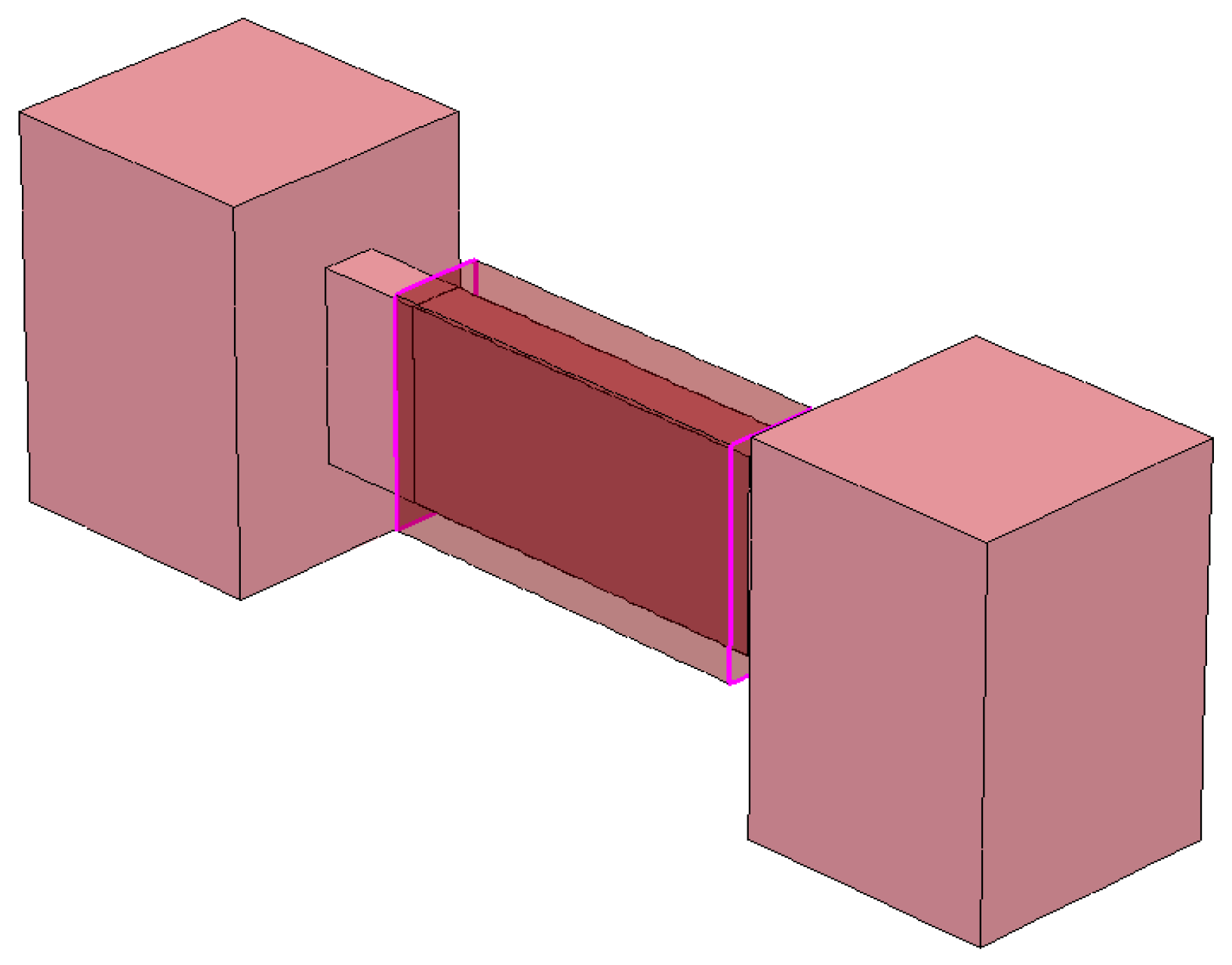
2.1. Simulation Environment

In this study, we used the TCAD Sentaurus Device (SDevice) to simulate the electrical and thermal characteristics of GAAFETs [7]. The device parameters of the GAAFET are summarized in Table 1 [8], and the electrical characteristics of the GAAFET in the simulation environment are listed in Table 2 [9,10,11]. In Refs. [9,10,11], the authors set the target specifications for the electrical characteristics that the GAAFETs are required to satisfy in the 5 nm technology node. The results of our simulations are also presented in Table 2. To satisfy the target electrical characteristics of the GAAFETs, various physics-related models and parameters were calibrated. The calibrated saturation velocity and the exponent in the high field saturation electron mobility model are used for the quasi-ballistic transport inside the very short channel structure [12]. In addition, the Lombardi mobility model for the consideration of Si/SiO2 interface, the lattice temperature-dependent mobility degradation model for the consideration of the SHE [13], the inversion/accumulation layer mobility model, and the thin-layer mobility model for the scaled channel [14] are used to calibrate the electrical characteristics, as has been documented in our previous work [2]. With these models, the thermodynamic transport model is applied simultaneously to consider the SHE conditions. With the thermodynamic transport model, the lattice temperature equation is simultaneously considered while solving the Poisson coupled drift–diffusion (DD) equation. Thus, the driving current is estimated by both the DD and lattice temperature equations, which corresponds to the current at the self-heating condition. For precise simulation of the SHE, various thermal-related parameters are defined in our simulation, based on the specifications in [15]. For the consideration of defining the thermodes of the device, proper thermal boundaries, including the thermal contact area and the thermal resistance at thermal contact, have to be considered. For the definition of thermal contacts, a temperature of 300 K is initially applied to the thermode contact. Thermodes in our simulated device are defined as the same region of electrical contact region, i.e., source, drain, and gate electrodes. Thus, the thermal effects by the input power have been evaluated under the same dimension as the contact area. Then, the thermal contact resistance of the thermode contact has been taken by referring to [16,17]. When compared with thermal contact resistance of [10], our estimated thermal contact resistance is 3.33 × 10⁶ K/W. By applying the thermal contact resistance with 3.33 × 10⁶, the simulated GAAFET is heated up to about 360 K at maximum, which is consistent with the result in [17]. The simulated structure of GAAFET, containing the lattice temperature distribution, is depicted in Figure 2. By referring to papers [16,17], the simulation for the consideration of proper thermal boundaries has been implemented. After simulation of the SHE, we extracted the thermal characteristics of the GAAFET from the TCAD results. From the DC simulation results, the RTH value was obtained using Equation (3). The CTH and τTH values were extracted using different rise time simulations after the AC transient simulation, which was previously introduced in [16] and also used in our previous work [8].

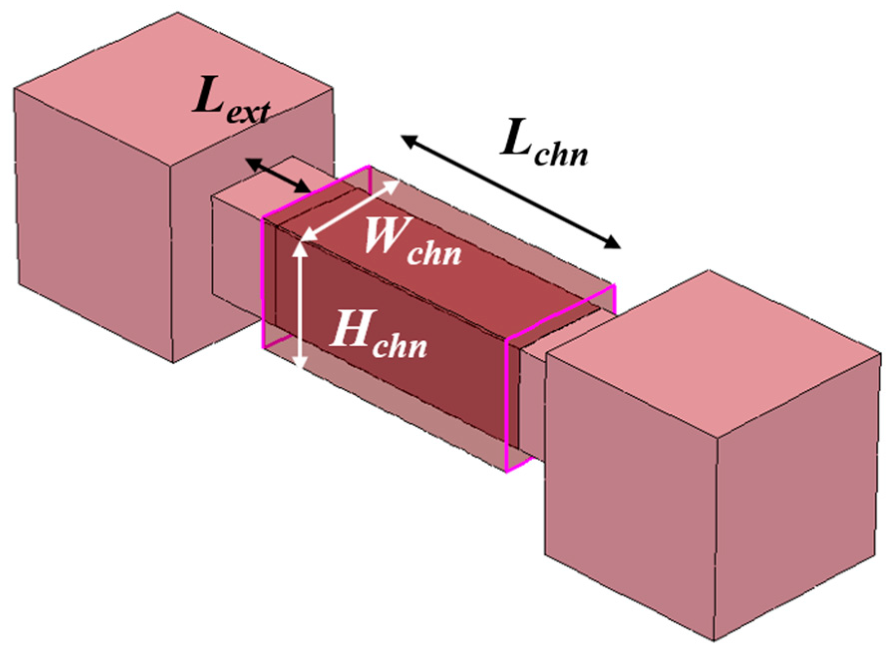
2.2. Thermal Characteristics of GAAFETs

The RTH of the device represents how much the device generates heat at the DC biased condition. Since higher heat induces frequent vibration of lattice atom, a decrease in electron mobility is observed when the device has a larger RTH. Thus, on-state current characteristic is related with the RTH parameter. On the other hand, CTH is activated at AC applied situation, for instance, pulsed input. Generated heat during the on-state of the pulse is stored at CTH and stored heat is released during the off-state of the pulse. Since larger CTH can store and release more heat, leakage current during the off-state of the pulse can be degraded by CTH. In short, RTH degrades on-state current and CTH degrades off-state current of the device. We used pulse signals to estimate the SHE when the GAAFET was operating under the AC conditions. Our simulated frequency of the pulses was at least 10 GHz; specifically, simulations were performed for 10, 25, and 50 GHz. When the AC pulse signal was applied to the gate electrode for gate bias, the corresponding lattice temperature generated by the SHE showed common RC delay properties. Figure 3 illustrates the relationship between the gate signal and the lattice temperature at different operating frequencies. As shown in Figure 3, the lattice temperature properties can be observed as RC delay characteristics, along with the gate voltages. Moreover, it is seen that the lattice temperature does not react quickly enough with the applied gate voltage at higher operating frequencies. In the RC-delayed case, this decrease in reaction speed occurs when the time constant is not small enough to fully follow the abrupt changes in gate voltage, especially at higher operating frequencies. In terms of the thermal characteristics, the time constant of the thermal response can be defined as the thermal time constant τTH. Similarly to the general circumstances of the RC circuit and system, τTH can be expressed as the product of RTH and CTH, as introduced with the equivalent thermal circuit of the device in [18]. A smaller τTH means faster response of the thermal properties. As shown in Figure 3b, at higher operating frequencies, the lattice temperature at the off-phase does not decrease to 300 K. This is critical for the off-phase leakage properties because the remaining heat generates extra carriers. Such thermally generated carriers degrade the leakage current properties during the off-phase of the pulse, which is originally of an extremely low current level, by creating a zero-bias state at the gate electrode. In Figure 4, the leakage current generation by the SHE at the off-phase is seen to increase. Thus, if we optimize the τTH properties and dissipate the heat effectively, the leakage current generation can be successfully suppressed even at higher operating frequencies. After modeling the τTH properties using a neural network, the genetic algorithm is used for the optimization of the neural network model to minimize the SHE.

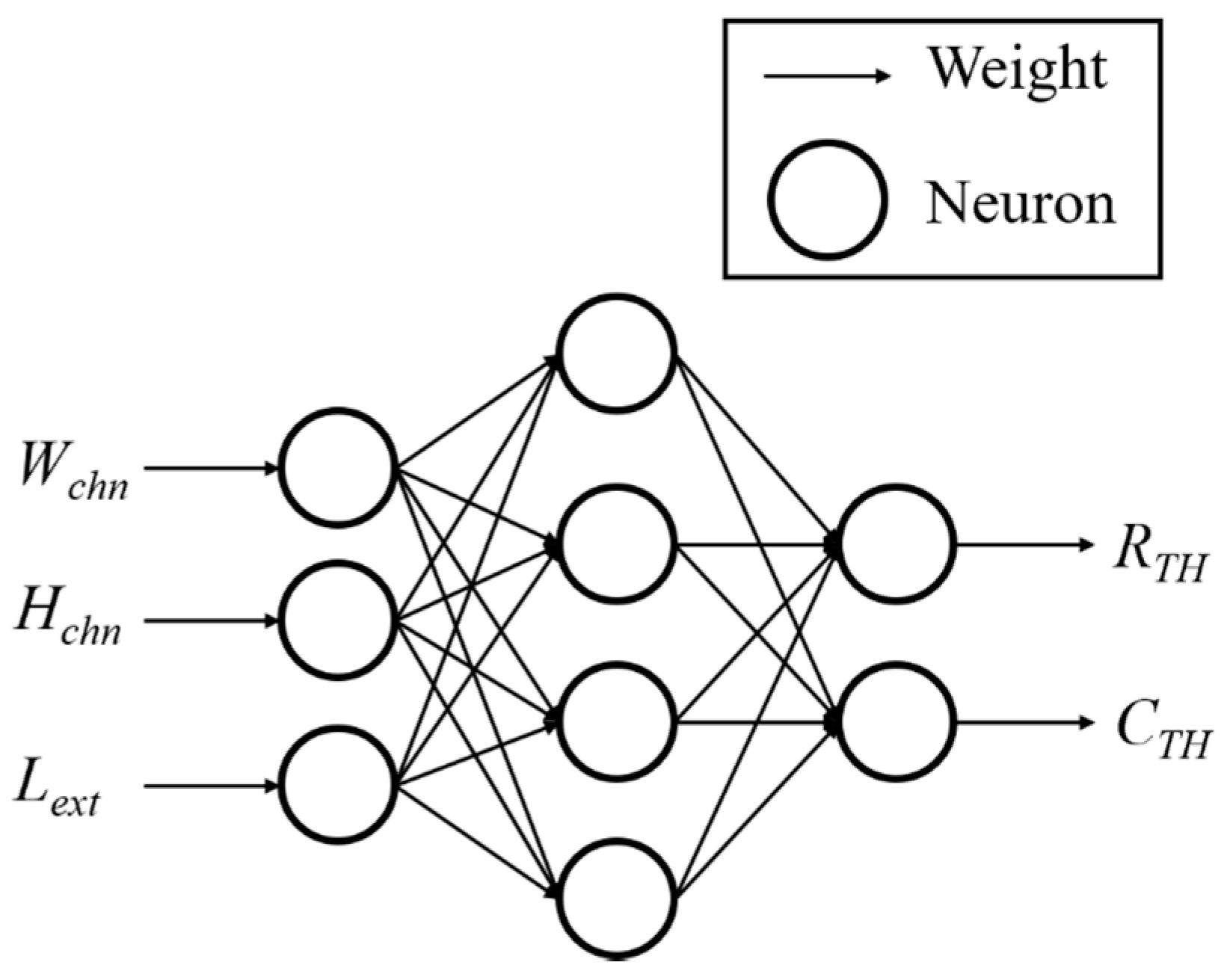
2.3. Neural Network Modeling

The neural network modeling of the thermal characteristics, RTH and CTH, was achieved using MATLAB from MathWorks. Figure 5 illustrates the schematic of the neural network model for prediction of the thermal characteristics. As shown in Figure 5, we set the device parameters as the input set of the model and the thermal characteristics as the output set. Since τTH is the product of RTH and CTH, we set the outputs of the model as RTH and CTH [8]. Thus, we simulated the means by which RTH and CTH could be influenced by varying the device parameters. The device parameters were varied in the range of 3–7 nm for both Wchn and Hchn, and in the range of 4–16 nm for Lext. From the TCAD simulations, the thermal characteristics (i.e., RTH, CTH, and τTH) were extracted. Using these extracted thermal parameters, the shallow neural network was trained to predict the thermal characteristics in accordance with structural variations. These three parameters were simulated with five divided points within the variation range, so that the training and testing of the network were implemented using a total of 125 (53) cases of non-replicated combinations of the input and output sets. We built the shallow neural network model using a single hidden layer with four hidden neurons, as shown in Figure 5. In our model, we used the tangent hyperbolic function shown in Equation (1) as the activation function [19].
f ( x ) = e 2 x 1 e 2 x + 1
Since the tangent hyperbolic function has relatively broader and larger slopes of the first-order derivatives, when compared with those of the common sigmoid function, the weight parameters of the network can be updated quickly with fewer errors, as reported in [19]. Thus, for training the data with speed and accuracy, the tangent hyperbolic function was used as the activation function in this study.
The network was trained via Bayesian regularization, as the training function to prevent large values of the weights; hence, our model showed well-controlled characteristics for the over-fitting problem, as shown in Figure 6. In Figure 6a, the τTH value, with respect to the device parameters in TCAD, shows a complicated surface response; thus, since the TCAD results of the τTH properties are complicated and unpredictable, modeling through the neural network method would be an appropriate solution for the highly sophisticated response. However, data-driven network training can be easily over-fitted, especially when trained to follow the response as a target with high variance and abrupt fluctuations, as shown in Figure 6a. The high variance of the model implies that the network is trained with higher values of the weight parameters. If there are no countermeasures for preventing such over-training, the model would exhibit generally over-trained properties, as seen in Figure 6b, which is an intentionally generated surface showing the properties of over-fitting. Therefore, if the model is over-fitted, the optimization process may be disadvantageous, or the model may not predict the apparent tendency of τTH variation appropriately. Since optimization on the over-trained surface might distort the optimization results and lower the accuracy of prediction, preventing over-training is one of the key points to consider in this work. As stated previously, the over-fitting problem can be suppressed when the model has a smaller variance, which is possible when the network is trained with smaller values of the weight parameters. In our modeling environment, we use the Bayesian regularization method as a countermeasure to prevent over-training, which assumes that the weight parameters follow a Gaussian distribution, with a mean of 0 and a standard deviation of σw. By this assumption, we set the weight parameters to be selected frequently near 0 during network training. Additionally, with the assumption of the Gaussian distribution of the weight parameters, the cost function can be expressed as follows:
C o s t ( w , b ) = 1 m i m ( t i y ( x i ) ) 2 + w 2 2 σ w 2 = β E D + α E W
where m, ti, y(xi), w, and σw are the number of data, the ith target data, the ith model output, the weight value, and the standard deviation of weight distribution conforming to the Gaussian profile, respectively.
From Equation (2), it is seen that the equation is a sum of two different quantities. The first is the sum of squared errors (SSE) and the other is the sum of squared weights (SSW). The SSE and SSW are expressed as ED and EW, with coefficients β and α (β + α = 1), respectively. If β is closer to 1, the network is trained to focus on smaller errors; however, if β < α, then the training process considers reducing the weight values rather than the errors. Thus, appropriate selection of β and α values is important when training the model. In this study, the method for estimation and calculation of β and α is derived from Refs. [20,21]. In accordance with Equation (2), the cost function has a penalty that is proportional to the SSW. Since the weight and bias values in the network are determined when the cost function is minimized by the backpropagation method [22], larger values of the weight parameters are rarely accepted, owing to the increased penalty in the cost function for larger weights. Using the restrictions where the weight values are distributed in a narrow range near 0 and the penalty in the cost function is as suggested in Equation (2), we build a generalized model with mechanisms for the prevention of over-fitting problems.
By the regularization on the network, it is seen in Figure 7 that the SSW of the network is much smaller than that without regularization algorithm. Figure 6c depicts the response of our neural network model surface for τTH prediction; a relatively softened surface response is observed, owing to the restriction of having high weights via Bayesian regularization. When compared with Figure 6b, which is intentionally generated for comparison, our model response is seen to be resistant to the over-fitting problem. Thereafter, we built a parameter-aware device prediction model for the thermal characteristics. Our model was constructed with a total of 125 combinations of independent input and output sets. Approximately 80% of the total datasets (i.e., 100 sets) were used to train the network, and the remaining 20% of datasets (i.e., 25 sets) were used for testing the trained network. The testing of the trained network was treated by evaluating the normalized mean squared error (NMSE) values. The prediction model for τTH shows the NMSE values of 0.0257 and 0.0276 after training and after testing, respectively. Since our NN model is generalized via the Bayesian regularization method, the test of how well our model is generalized was also treated with an NMSE evaluation. The NMSE test was taken on the random samples that are located outside the training boundary. The tested NMSE values for the outside samples were 0.476 with regularization and 2.708 without regularization. Thus, it is observed that the generalized NN model can be obtained from our modeling method.

2.4. Optimization under Constrained Conditions

As shown in Figure 8, the τTH properties with variations in the device parameters show complicated and highly nonlinear results; thus, it would be laborious to find the minimum value from such a surface when using the general method. Since the genetic algorithm is well known for its effectiveness in finding the minimum or maximum values at certain surfaces among multiple variables, while also avoiding local minima or maxima, we used the genetic algorithm to optimize the model.
Figure 9 describes the optimization scheme of the genetic algorithm in our manuscript. For optimization by the genetic algorithm, various parameters related with optimization process were used. For the selection, the tournament selection function was used and the selection parameter—the selection tournament size—was 2. A crossover fraction of 0.8 was used for crossover. At last, the mutation parameter (the mutation rate) was set to be 0.01 (1%).
From our previous work on the SHEs of FinFETs and GAAFETs, both were seen to have increased RTH values and decreased CTH values with scaled-down channel parameters. Since GAAFETs inherently have larger RTH values than FinFETs, mainly owing to the extremely small structures of GAAFETs, the RTH of GAAFETs should be carefully considered [8]. From the structural properties, the heat generated by the SHE in the channel was dissipated through the surface area of the channel; thus, RTH was inversely proportional to the surface area of the channel [23]. From the relation between the RTH and surface area, we set the linear constrained condition on the genetic algorithm (i.e., the surface area of the channel was always constant), to prevent the increase of RTH and maintain its initial value during optimization. The constrained condition was that the sum of Wchn and Hchn was 10 nm, which corresponded to the same value of the sum of these parameters in the reference structure, as shown in Table 1. By applying the genetic algorithm within the training boundary on the τTH prediction neural network model, we attempted to find the minimum value of τTH, which w the representative value for the SHE evaluation.

3. Results and Discussion

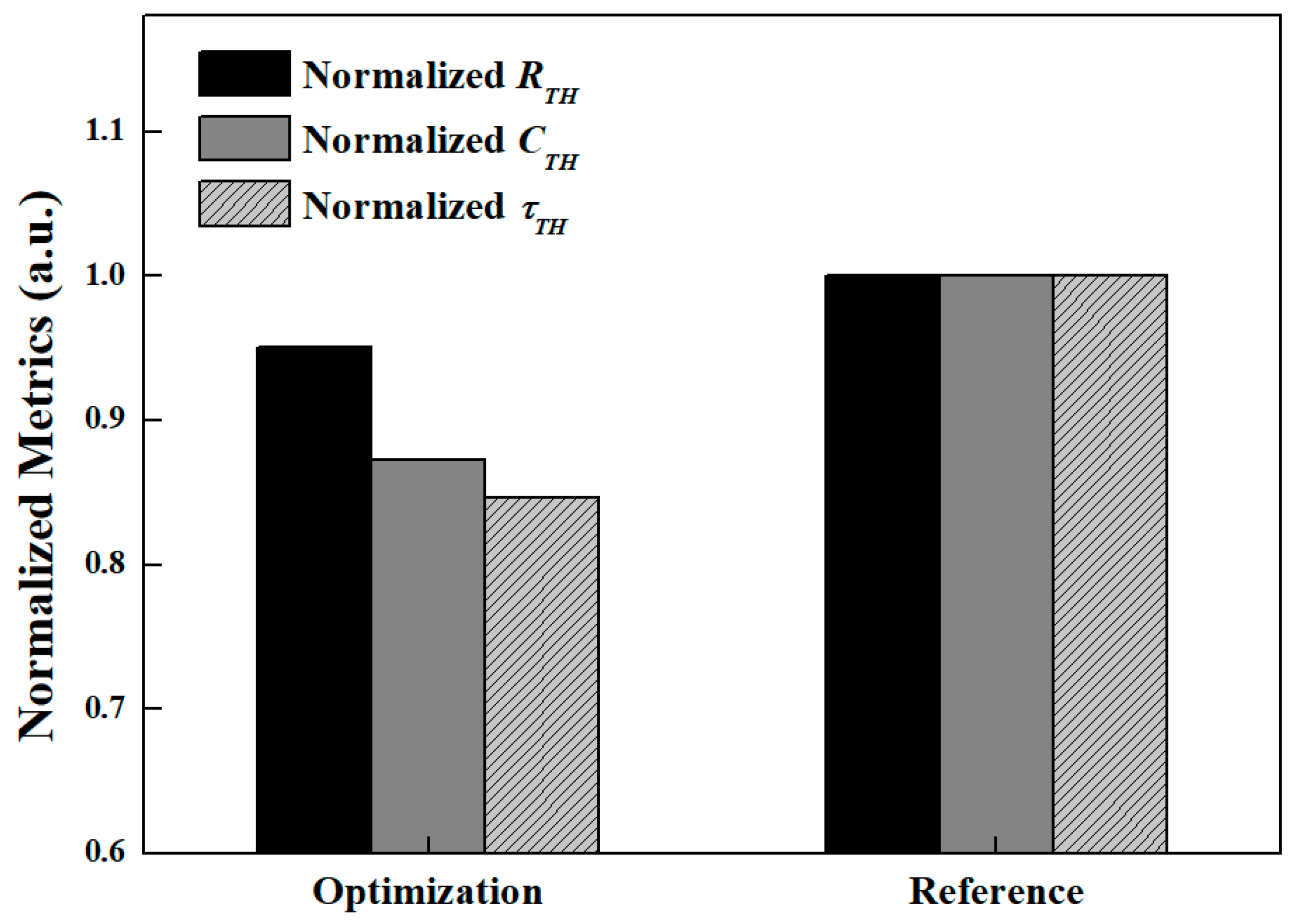
3.1. Optimization Results from Genetic Algorithm

Table 3 shows the optimization results of the genetic algorithm, with a total of 102 epochs, which represent the fitness value at each epoch. As it can be seen in Table 3, the optimal value of τTH was observed as the epoch goes on. Owing to the linear constratined condition that prevented the RTH from increasing, the sum of Wchn and Hchn was always limited to 10 nm, as shown in Table 3. It can be seen that, during the optimization process, the τTH characteristics showed improved tendencies when Lext was minimized and the channel had a nanosheet-like structure. Specifically, when the channel parameters, Wchn and Hchn, were split as 3 nm and 7 nm instead of 5 nm and 5 nm, respectively, the extension length converged to the lower limit of the training and optimization boundary, and the τTH characteristics were improved. Since our targeted GAAFET is designed for 5 nm node technology, the linear constrained condition on the genetic algorithm—which limited the sum of Wchn and Hchn to 10 nm—was applied to optimize the device charateristics within the design space of technology node specification. By doing so, the thermal characteristics of the target GAAFET were optimized within the technology node of 5 nm. It was observed that the optimized device parameters were settled in the edge of the training and optimization boundaries. This result can be analysed as a result of regularization on the neural network model and the constrained condition on the optimizing algorithm. Since we used a smoothed surface model by regularization during the optimzation process, there was less possibility of finding an optimum point within the optimization space. As well as the regularization of our model, the constrained condition on the genetic algorithm also contributed to the emigration of the optimum point. The constrained condition—which limited the sum of Wchn and Hchn to 10 nm—made the genetic algorithm explore along the line that satisfied the constrained condition in the neural network model. Thus, limited optimization results were obtained, when compared with the results from entire surface model; however, the linear constrained condition in our work is inevitable, since Weff had to be fixed as a node specification. Thus, optimization results, split at the edge of training boundary, are observed.
Our model predicts the optimized τTH value as 32.25 ps, as listed in Table 4, which is a precise result when compared to the TCAD result of 31.91 ps, showing an error of about 1.06%. Moreover, in the evaluation of the other characteristics of the SHE (i.e., RTH and CTH) it was shown that the RTH and CTH values can be precisely predicted by the neural network model, as shown in Table 4. Figure 10 depicts the predicted structure of the GAAFET after optimization by the genetic algorithm.

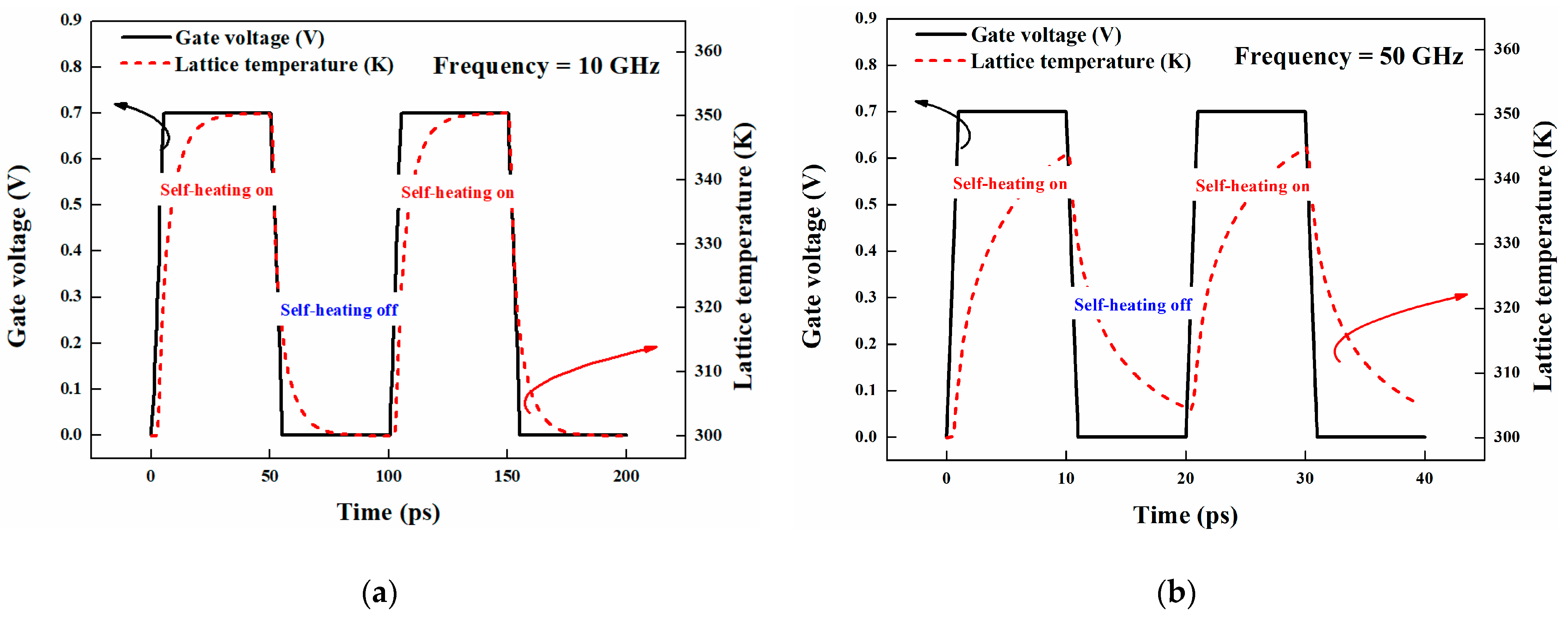
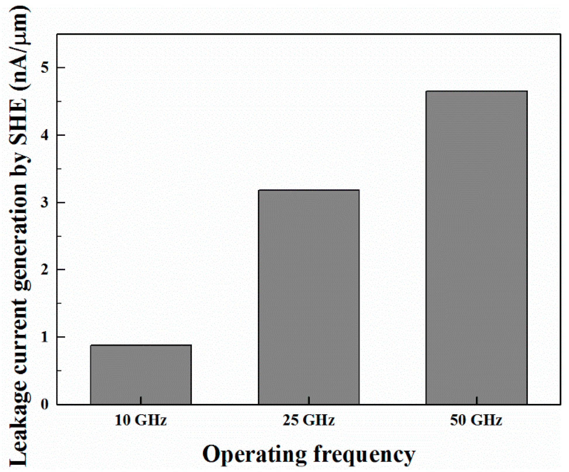
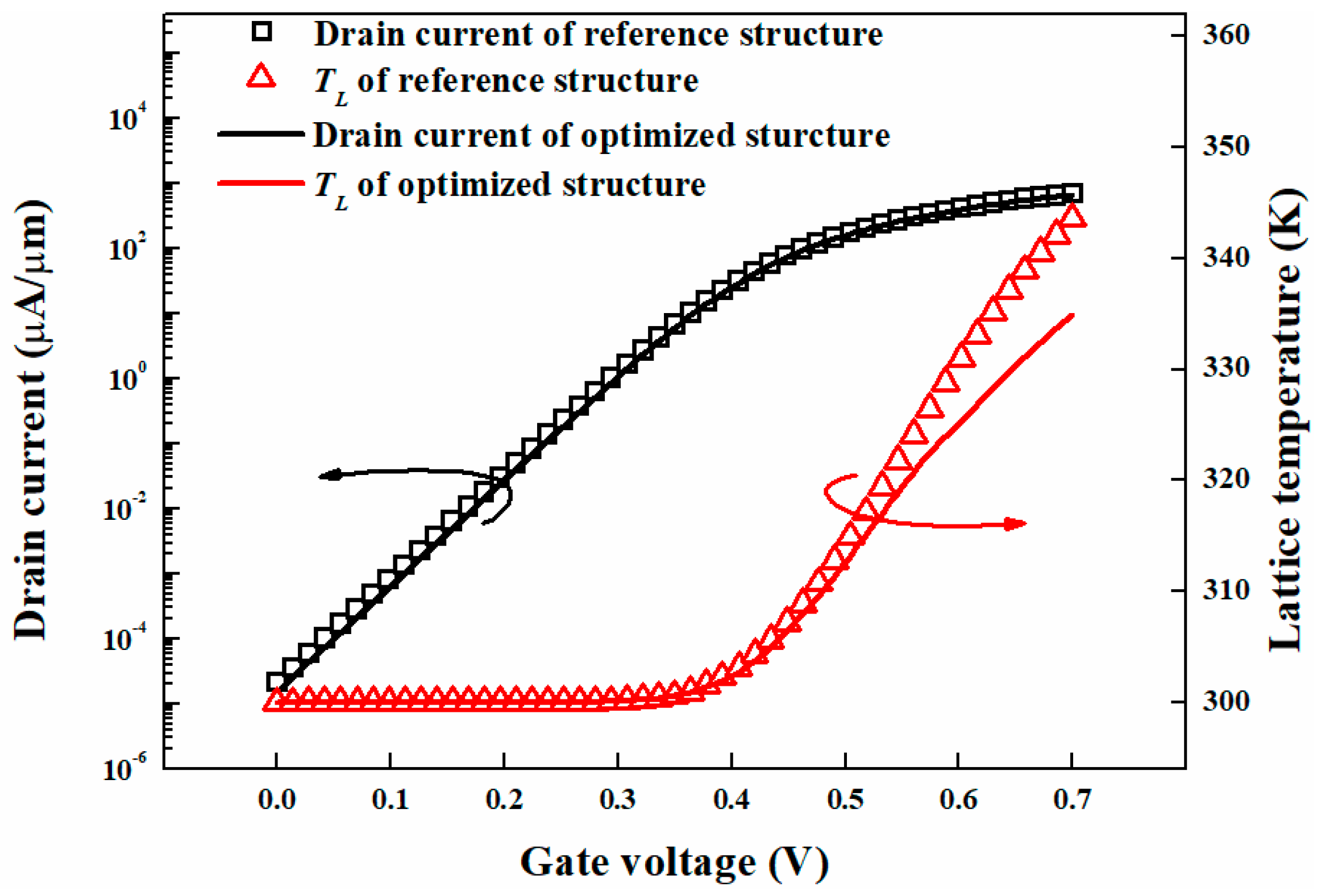
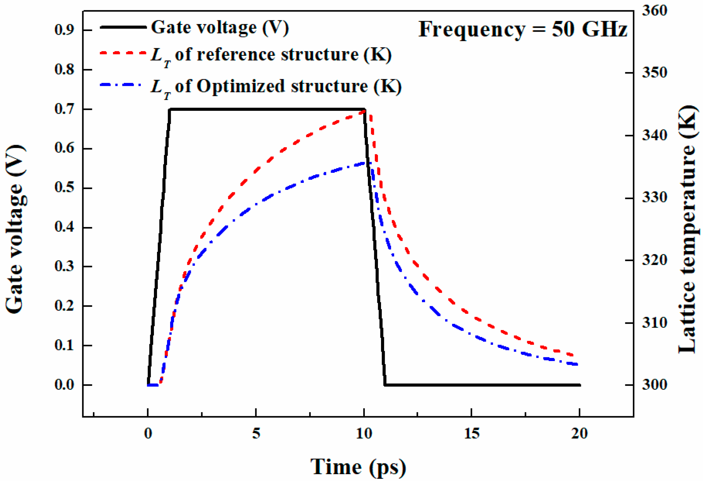
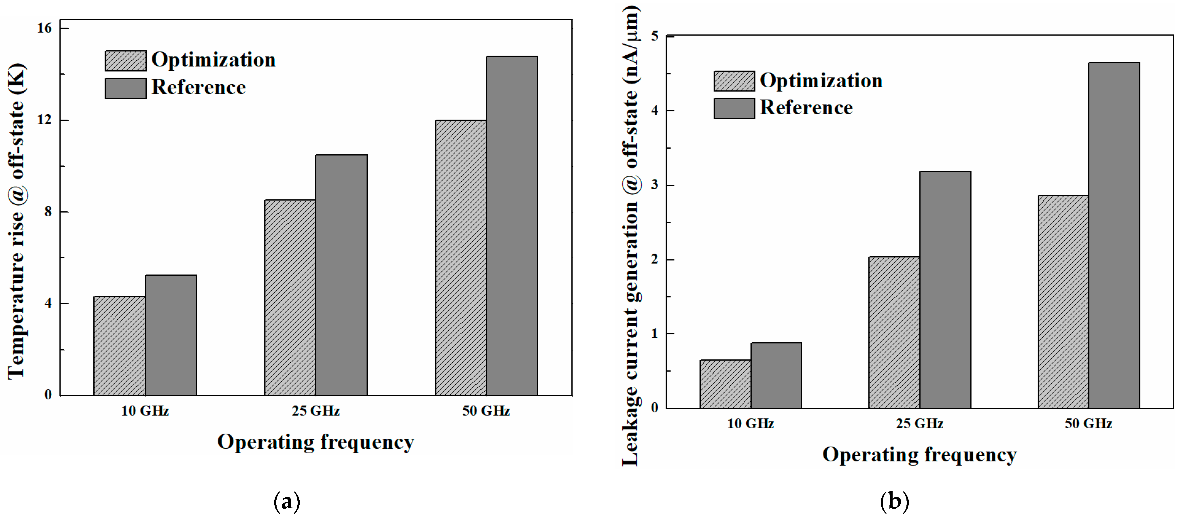
3.2. Thermal Characteristics after Optimization

Figure 11 shows that the optimized structure has a smaller τTH than the reference structure. The reference structure in the figure also indicates the structure before the optimization, which is also depicted in Figure 1. As seen in the figure, the RTH value remains almost unchanged (~5%) but perhaps slightly decreased, which is the result of the constrained condition of the algorithm. Unlike the trend of the RTH, the optimized structure has a relatively decreased CTH value, which contributes to the reduction of τTH. Since the heat generated by the SHE is confined and transported within the volume of the channel (Vchn), the heat capacity is proportional to the Vchn. As shown in Figure 12, the optimized structure has a smaller channel volume than the reference structure of the GAAFET. Furthermore, it can be seen from Figure 12 that the decrease in CTH is similar to the decrease in Vchn. Thus, the decrease in the channel volume after optimization is the main contributor to the smaller CTH value, which results in the decrease in τTH properties. The thermal characteristics before and after optimization are compared in Figure 13 and Figure 14.
In Figure 13, the DC characteristics of the SHE are examined by sweeping the DC voltage at the gate electrode from 0 to VDD (0.7 V); further, the drain current to gate voltage (I–V) transfer characteristics are illustrated with lattice temperature information. It is observed that the drain current properties before and after optimization are only slightly changed. In terms of the lattice temperature, the optimized sturcture shows improved characteristics for thermal generation. As seen in Figure 13, the temperature rise inside the device is suppressed while maintaining the operating current, which is directly related to the DC power. This means that the opimized device generates less heat than the reference structure for similar levels of DC power consumption [24]. From Equation (3):
R T H = Δ T Input   DC   power   [ K / W ]  
where less heat generation at a similar DC power consumption implies that a smaller RTH [8] can be achieved.
From the results shown in Figure 13, it can be concluded that the optimized structure—which is the nanosheet-shaped channel with a rectangular structure and extension region—has more effective properties for the disspation of heat than the reference structure (owing to the broad structures of the channel and extension) while having the same channel surface area. Thus, as shown in Figure 12 and Equation (3), the optimized structure achieves a relatively smaller RTH, which is consistent with the results in Figure 11.
The lattice temperature properties with propagation of the AC pulse as gate bias, after the optimzation process, are presented in Figure 14 for both the optimized and the reference structures. In Figure 14, the rise in the maximum lattice temperature by the SHE is suppressed after optimization, and a smaller temperature rise at the off-phase of the pulse is observed. Less temperature increase in the off-phase of the pulse indicates that the thermally generated leakage current can be successfully suppressed after optimization.
Figure 15 presents comparisons between the SHEs for both the optimized structure and the reference structure, in terms of lattice temperature increase and leakage current generation. Figure 15a shows comparisons between the temperature increases at the off-phase of the pulse, before and after optimization; here, less increase in the lattice temperature is observed at the optimized structure for each operating frequency. As the operating frequency increases, there is a corresponding increment in lattice temperature; however, the decreases in the rates of temperature rise after optimization are similar (about 20%) for each of the operating frequencies, i.e., 10, 25, and 50 GHz. Thus, we could suppress the increase in lattice temperature by about 20% when the optimized device was biased with an AC pulsed signal. Figure 15b shows the optimization results for the leakage current generation at the off-phase of the pulse by the SHE. It can be seen that the leakage current generation is also suppressed according to the suppression in temerpature rise, similar to that in Figure 15a. It is worth noting here that the leakage current generation is suppressed by about 40% at the opreating frequency of 50 GHz after optimization. Thus, we could improve the thermal generation and leakage current properties induced by the SHE of the GAAFET by modeling and optimizing the thermal time constant τTH.
The results of the optimization of the neural network model, under the linear constrained conditions, indicate that optimization is achieved when the shape of the channel has a nanoscaled sheet-shaped structure. The device parameters after optimization are noted as 3 nm, 7 nm, and 4 nm for Wchn, Hchn, and Lext, respectively. Compared with the reference structure and parameters shown in Figure 1 and Table 1, the RTH value remains almost unchanged between the reference and the optimized structures—i.e., the RTH value change after optimization was <5%—mainly owing to the additional linear constrained condition applied to the genetic algorithm. On the other hand, in the case of the CTH, the optimized structure has a smaller value with almost a 13% reduction in the CTH value seen after optimization, which eventually reduces the τTH properties by almost 15%. As seen in Figure 11, τTH is reduced by about 15% after optimization, which means that the device now dissipates heat more quickly to the increased lattice temperature by the SHE. Thus, the rise in lattice temperature and the generation of off-state leakage current by the SHE are also suppressed by up to 40% at the operating frequency of 50 GHz, in addition to the reduction of τTH.

4. Conclusions

In this study, the thermal characteristics of GAAFETs were modeled via a shallow neural network modeling method. By applying the genetic algorithm with a linear constrained condition to the neural network model, the thermally aware network was optimized. Herein, we suggested an optimized structure of the GAAFET based on the genetic algorithm, which had the smallest τTH value within the constrained boundary. Based on the results of the optimization of the thermal characteristics, the τTH value was reduced by about 15%, which suppressed the rise in lattice temperature by the SHE by about 20%. Thus, less current generation was observed at the off-phase of the pulse via modeling and optimization of the τTH properties. In our work, the optimization of the output characteristics is achieved using the neural network modeling method and a genetic algorithm. Further, the optimization of the semiconductor device in this work is achieved using only a restricted dataset, which was extracted from TCAD simulations.

Author Contributions

Writing—original draft preparation, C.P. and I.Y.; writing—review and editing, C.P. and I.Y.; Conceptualization, C.P.; methodology, C.P.; investigation, C.P.; supervision, I.Y.; project administration, I.Y. All authors have read and agreed to the published version of the manuscript.

Funding

This work was supported by the Institute of BioMed-IT, Energy-IT, and Smart-IT Technology (BEST), a Brain Korea 21 plus program at Yonsei University. And The APC was supported by Y-BASE R&E Institute, a Brain Korea 21 four program, Yonsei University.

Acknowledgments

This work has been supported by Y-BASE R&E Institute, a Brain Korea 21 four program, Yonsei University. The electronic design automation (EDA) tool was also supported by the IC Design Education Center (IDEC), Seoul, Korea.

Conflicts of Interest

The authors declare no conflict of interest.

References

  1. Ko, K.; Lee, J.K.; Kang, M.; Jeon, J.; Shin, H. Prediction of process variation effect for ultrascaled GAA vertical FET devices using a machine learning approach. IEEE Trans. Electron Devices 2019, 66, 4474–4477. [Google Scholar] [CrossRef]
  2. Lim, J.; Shin, C. Machine Learning (ML)-Based Model to Characterize the Line Edge Roughness (LER)-Induced Random Variation in FinFET. IEEE Access 2020, 8, 158237–158242. [Google Scholar] [CrossRef]
  3. Mehta, K.; Wong, H.-Y. Prediction of FinFET Current-Voltage and Capacitance-Voltage Curves using Machine Learning with Autoencoder. IEEE Electron Device Lett. 2020, 42, 136–139. [Google Scholar] [CrossRef]
  4. Moroz, V.; Smith, L.; Huang, J.; Choi, M.; Ma, T.; Liu, J.; Zhang, Y.; Lin, X.-W.; Kawa, J.; Saad, Y. Modeling and optimization of group IV and III–V FinFETs and nano-wires. In Proceedings of the 2014 IEEE International Electron Devices Meeting, San Francisco, CA, USA, 15–17 December 2014; pp. 7.4.1–7.4.4. [Google Scholar]
  5. Wong, H.Y.; Xiao, M.; Wang, B.; Chiu, Y.K.; Yan, X.; Ma, J.; Sasaki, K.; Wang, H.; Zhang, Y. TCAD-machine learning framework for device variation and operating temperature analysis with experimental demonstration. IEEE J. Electron Devices Soc. 2020, 8, 992–1000. [Google Scholar] [CrossRef]
  6. Park, J.; Lee, J.K.; Shin, H. Machine learning method to predict threshold voltage distribution by read disturbance in 3D NAND Flash Memories. Jpn. J. Appl. Phys. 2020, 59, 081003. [Google Scholar] [CrossRef]
  7. Sentaurus Device User Guide, Version L-2016.03; Synopsys TCAD Sentaurus: San Jose, CA, USA, 2016.
  8. Park, C.; Yun, I. Degradation of off-phase leakage current of FinFETs and Gate-All-Around FETs Induced by the self-heating effect in the high-frequency operation regime. IEEE Trans. Nanotechnol. 2020, 19, 308–314. [Google Scholar] [CrossRef]
  9. Wu, Y.-C.; Jhan, Y.-R. Introduction of synopsys sentaurus TCAD simulation. In 3D TCAD Simulation for CMOS Nanoeletronic Devices; Springer: Berlin/Heidelberg, Germany, 2018; pp. 1–17. [Google Scholar]
  10. Yoon, J.-S.; Lee, S.; Yun, H.; Baek, R.-H. Digital/Analog Performance Optimization of Vertical Nanowire FETs Using Machine Learning. IEEE Access 2021, 9, 29071–29077. [Google Scholar] [CrossRef]
  11. Zheng, P.; Connelly, D.; Ding, F.; Liu, T.-J.K. FinFET evolution toward stacked-nanowire FET for CMOS technology scaling. IEEE Trans. Electron Devices 2015, 62, 3945–3950. [Google Scholar] [CrossRef]
  12. Bude, J. MOSFET modeling into the ballistic regime. In Proceedings of the 2000 International Conference on Simulation Semiconductor Processes and Devices (Cat. No. 00TH8502), Seattle, WA, USA, 6–8 September 2000; pp. 23–26. [Google Scholar]
  13. Karlik, B.; Olgac, A.V. Performance analysis of various activation functions in generalized MLP architectures of neural networks. Int. J. Artif. Intell. Expert Syst. 2011, 1, 111–122. [Google Scholar]
  14. Khandelwal, S.; Duarte, J.P.; Medury, A.S.; Venugopalan, S.; Paydavosi, N.; Lu, D.D.; Lin, C.-H.; Dunga, M.; Yao, S.; Morshed, T. BSIM-CMG 110.0.0: Multi-Gate MOSFET Compact Model: Technical Manual; BSIM Group UC Berkeley: Berkeley, CA, USA, 2015. [Google Scholar]
  15. Kompala, B.K.; Kushwaha, P.; Agarwal, H.; Khandelwal, S.; Duarte, J.-P.; Hu, C.; Chauhan, Y.S. Modeling of nonlinear thermal resistance in FinFETs. Jpn. J. Appl. Phys. 2016, 55, 04ED11. [Google Scholar] [CrossRef]
  16. Kumar, U.S.; Rao, V.R. A thermal-aware device design considerations for nanoscale SOI and bulk FinFETs. IEEE Trans. Electron Devices 2015, 63, 280–287. [Google Scholar] [CrossRef]
  17. Lombardi, C.; Manzini, S.; Saporito, A.; Vanzi, M. A physically based mobility model for numerical simulation of nonplanar devices. IEEE Trans. Comput.-Aided Des. Integr. Circ. Syst. 1988, 7, 1164–1171. [Google Scholar] [CrossRef]
  18. Myeong, I.; Son, D.; Kim, H.; Shin, H. Analysis of self heating effect in DC/AC mode in multi-channel GAA-field effect transistor. IEEE Trans. Electron Devices 2019, 66, 4631–4637. [Google Scholar] [CrossRef]
  19. Reggiani, S.; Gnani, E.; Gnudi, A.; Rudan, M.; Baccarani, G. Low-field electron mobility model for ultrathin-body SOI and double-gate MOSFETs with extremely small silicon thicknesses. IEEE Trans. Electron Devices 2007, 54, 2204–2212. [Google Scholar] [CrossRef]
  20. Wang, L.; Brown, A.R.; Nedjalkov, M.; Alexander, C.; Cheng, B.; Millar, C.; Asenov, A. Impact of self-heating on the statistical variability in bulk and SOI FinFETs. IEEE Trans. Electron Devices 2015, 62, 2106–2112. [Google Scholar] [CrossRef] [Green Version]
  21. Foresee, F.D.; Hagan, M.T. Gauss-Newton approximation to Bayesian learning. In Proceedings of the International Conference on Neural Networks (ICNN’97), Houston, TX, USA, 12 June 1997; pp. 1930–1935. [Google Scholar]
  22. Hecht-Nielsen, R. Theory of the backpropagation neural network. In Neural Networks for Perception; Elsevier: Amsterdam, The Netherlands, 1992; pp. 65–93. [Google Scholar]
  23. Makovejev, S.; Olsen, S.; Raskin, J.-P. RF extraction of self-heating effects in FinFETs. IEEE Trans. Electron Devices 2011, 58, 3335–3341. [Google Scholar] [CrossRef]
  24. Park, C.; Yun, I. Thermal modeling of 7 nm node bulk fin-shaped field-effect transistors for device structure-aware design. Semicond. Sci. Technol. 2018, 33, 115014. [Google Scholar] [CrossRef]
Figure 1. 3D structure of simulated GAAFET.
Electronics 10 02570 g001
Figure 2. Distribution of lattice temperature at self-heating condition: @ VGS = VDS = 0.7 V.
Electronics 10 02570 g002
Figure 3. Lattice temperature response to the gate voltage of (a) 10 GHz and (b) 50 GHz.
Electronics 10 02570 g003
Figure 4. Leakage current generation by the SHE at the off-phase of the pulse.
Electronics 10 02570 g004
Figure 5. Schematic of a neural network model for thermal characteristics.
Electronics 10 02570 g005
Figure 6. Comparison of responses of the (a) TCAD surface, (b) intentionally over-trained neural network surface, and (c) our neural network surface.
Electronics 10 02570 g006
Figure 7. Trend of SSW along with training epoch, with and without regularization.
Electronics 10 02570 g007
Figure 8. Scatter plot of thermal time constant, along with variation of (a) Wchn and Hchn, (b) Wchn and Lext.
Electronics 10 02570 g008
Figure 9. Optimization flow of genetic algorithm.
Electronics 10 02570 g009
Figure 10. Structure of the GAAFET after optimization using genetic algorithm.
Electronics 10 02570 g010
Figure 11. Optimization results of RTH, CTH, and τTH properties.
Electronics 10 02570 g011
Figure 12. Relation between the channel volume (Vchn) and CTH for the optimization and reference GAAFET structures.
Electronics 10 02570 g012
Figure 13. DC applied to the gate characteristics of the SHE, before and after optimization.
Electronics 10 02570 g013
Figure 14. AC applied gate characteristics of the SHE, before and after optimization.
Electronics 10 02570 g014
Figure 15. Comparison between: (a) the temperature rise by the SHE between the optimized and the reference structures; (b) corresponding leakage current generation at the off-phase of the pulse between the optimized and the reference structures.
Electronics 10 02570 g015
Table 1. Device parameters.
ParameterGAAFET
Channel length (Lchn)15 nm
Channel Width (Wchn)5 nm
Channel Height (Hchn)5 nm
Extension length (Lext)4 nm
Effective Oxide Thickness (EOT)0.8 nm
Source/Drain Doping 1 × 10 20 cm−3
Channel Doping 1 × 10 15 cm−3
Table 2. Electrical properties used in the simulation.
ParameterGAAFET from [3,4,5]GAAFET, Our Simulation
VDD0.7 V0.7 V
Ion.sat610–702 μA/μm695 μA/μm
Ioff.sat20 pA/μm21 pA/μm
Vth0.3–0.4 V0.35 V
SS64–71 mV/dec62.76 mV/dec
Table 3. Optimization results from the genetic algorithm on the neural network model.
Wchn [nm]Hchn [nm]Lext [nm]τTH [ps]
7.003.0023.1558.96
6.883.1223.0958.70
5.964.0421.8557.11
5.454.4518.6455.53
3.106.909.5543.46
3.066.944.2533.09
3.007.004.0032.25
3.007.004.0032.25
Table 4. Comparison of TCAD and GA results.
TCAD ResultGA Result
Wchn [nm]33
Hchn [nm]77
Lext [nm]44
RTH [K/μW]4.094.16
CΤH [zJ/K]7.877.75
τTH [ps]31.9132.25
Publisher’s Note: MDPI stays neutral with regard to jurisdictional claims in published maps and institutional affiliations.

