Article

Design of a Compact Ultra-Wideband Bandpass Filter Using Inductively Compensated Parallel-Coupled Lines

by
Meechai Jamsai
1,
Niwat Angkawisittpan
1,2,* and
Adisorn Nuan-On
1,2
1
Department of Electrical and Computer Engineering, Faculty of Engineering, Mahasarakham University, Maha Sarakham 44150, Thailand
2
Research Unit for Computational Electromagnetics and Optical Systems (CEMOS), Faculty of Engineering, Mahasarakham University, Maha Sarakham 44150, Thailand
*
Author to whom correspondence should be addressed.
Electronics 2021, 10(21), 2575; https://doi.org/10.3390/electronics10212575
Submission received: 20 September 2021 / Revised: 17 October 2021 / Accepted: 19 October 2021 / Published: 21 October 2021

Abstract

:
An ultra-wideband bandpass filter (UWB-BPF) using inductively compensated parallel-coupled lines (ICPCL) is presented in this article. It consists of three circuits: a high-pass filter (HPF), a lowpass filter (LPF), and a transmission line. The HPF and the LPF are independently synthesized from the ICPCL. The proposed filter can suppress unwanted frequencies in the upper stopband and increase the skirt slope of the frequency response in the transition bands. The fabricated UWB-BPF with compact size provides good passband performances, with insertion loss of better than −0.49 dB and return loss of better than −12 dB in the frequency range of 2.92–10.95 GHz (the bandwidth of 8.03 GHz). The 107% bandwidth is achieved. In addition, the proposed filter can suppress the spurious frequencies at 2f0, which is greater than 30 dB. The measured results accord well with the simulation results. The novelty of the paper is the introduction of the ICPCL for the construction of the compact UWB-BPF.

1. Introduction

In recent years, wireless microwave communication systems have played a significant role in our daily activities. The Federal Communications Commission defined that the commercial communications could apply the 3.10–10.60 GHz frequency band for their uses in 2002. UWB-BPF has been paid attentions from research communities and industries [1]. Several circuits and techniques have been developed to operate in this frequency band [2,3,4,5,6,7,8,9,10,11,12,13]. In [4], a composite microstrip bandpass filter with more than 100% bandwidth is introduced. An HPF and an LPF are embedded into each other to increase the efficiency of the circuit as a bandpass filter (BPF) by applying stubs for tuning the passband. In [5], two-section open-circuited stubs are applied to synthesize UWB filters using the Z-transformation technique to achieve sharp attenuations. In [6], UWB filters are synthesized by cascading an HPF and an LPF. The HPF is fabricated from interdigital capacitors and short-circuited stubs while the defected ground structure arrays are used to fabricate the LPF. It achieves a 20 dB attenuation with a wide stopband. In [10], a branch-line with transmission lines is applied to synthesize UWB-BPF. In [11], a stepped-impedance stub is employed to generate the UWB-BPF. Additionally, triple-mode stepped resonators are applied to design the UWB filters using triple-notched bands [12]. Normally, UWB-BPFs are simple to design and they apply a stub transmission line for fine-tuning of the circuit’s frequency band [14,15]. The UWB-BPF is used to filter harmonic frequencies from the circuit’s output. Therefore, the filter design focuses on improving the circuit’s frequency response to achieve wide stopbands. The filters should provide a high skirt slope of the frequency response in the transition frequency ranges, low insertion loss, and high return loss. In previous studies, the circuit design applied transmission lines with high impedances and low impedances which were cascaded to form filter circuits [16,17,18]. It turned out the circuits were large.
There are many applications of ICPCL in the research community. In [19], the ICPCL is applied for designing multi-section parallel-coupled lines, Lange couplers, and Marchand Baluns. In addition, this technique is used to design the microstrip parallel-coupled lines (PCL) with high directivity in [20]. The advantages of the inductively compensated technique are that the compact size of the design circuit is achieved, and the fabrication process is easy.
In the proposed work, an UWB-BPF is developed to achieve a high skirt slope of the frequency response in the transition frequency ranges, low insertion losses, high return losses, and compact size. The HPF and the LPF are independently constructed with the ICPCL. The HPF, the LPF, and the transmission line are cascaded for synthesizing the proposed filter. In the design, The HPF can suppress the frequency range in the lower stopband of the proposed UWB-BPF while The LPF can suppress the frequency range in the upper stopband of the proposed UWB-BPF. Fortunately, the spurious frequency at 2fo is in the range of the upper stopband. The spurious frequency at 2fo can be eliminated. To design the appropriate cut-off frequencies, the cut-off frequency of the HPF must be lower than the cut-off frequency of the LPF. The novelty of this paper is to extend the study of the ICPCL [19,20] to design the UWB-BPF with mathematical equations for electrical length calculation. In this article, Section 2 describes the design of the proposed UWB-BPF. Section 3 demonstrates the measured results and discussions of the proposed UWB-BPF. The conclusions are provided in Section 4.

2. The Construction of the Proposed UWB-BPF

The construction of the proposed UWB-BPF is presented in this section. The technique starts with the design of the ICPCL. The design of the ICPCL is used to synthesize the HPF and the LPF. The proposed UWB-BPF is constructed by cascading the HPF, the transmission line, and the LPF. To obtain simulated results of the HPF, the LPF, and the proposed UWB-BPF, CST Studio Suite is used to simulate the design [21]. The details of the design are shown as follows.

2.1. The ICPL

The ICPCLs are used to synthesize the HPF and the LPF in this work because it can obtain high suppression performances in the stopbands and high directivity from the ICPCL [19,20]. The ICPCLs are achieved by adding compensated inductors ( L p ) to a conventional PCL, as shown in Figure 1.
In previous techniques [18,20,22,23], perfect isolation performance at the operating frequency ( f 0 )   can be achieved ( S 31 ( f 0 )   = 0), which results in an increasing directivity for the ICPCL. From [23], it finds that the equation for the compensated impedance ( Z L p ) is:
  Z L p = Z c e ( Z c o 2 + Z c 2 ) s i n h   θ 0 + Z c o ( Z c e 2 + Z c 2 ) s i n h   θ e 2 Z c 3 A Z c ( Z c e s i n h θ 0 + Z c o s i n h θ e ) Z c 2 A ,
  • where A = c o s h   θ e c o s h   θ o
  • Z c is characteristic impedance,
  • Z c e is even-mode characteristic impedance,
  • Z c o is odd-mode characteristic impedance,
  • ε e f f e is even-mode effective dielectric constant,
  • ε e f f o is odd-mode effective dielectric constant,
  • θ e is even-mode electrical length ( = π 2 ),
  • θ o is odd-mode electrical length ( = π 2 ϑ ),
  • and ϑ = ε e f f o ε e f f e .
From Equation (1), the compensated inductance could be expressed by the following equation:
L p = 1 2 π f 0 I m { Z L p } .

2.2. Design of the HPF

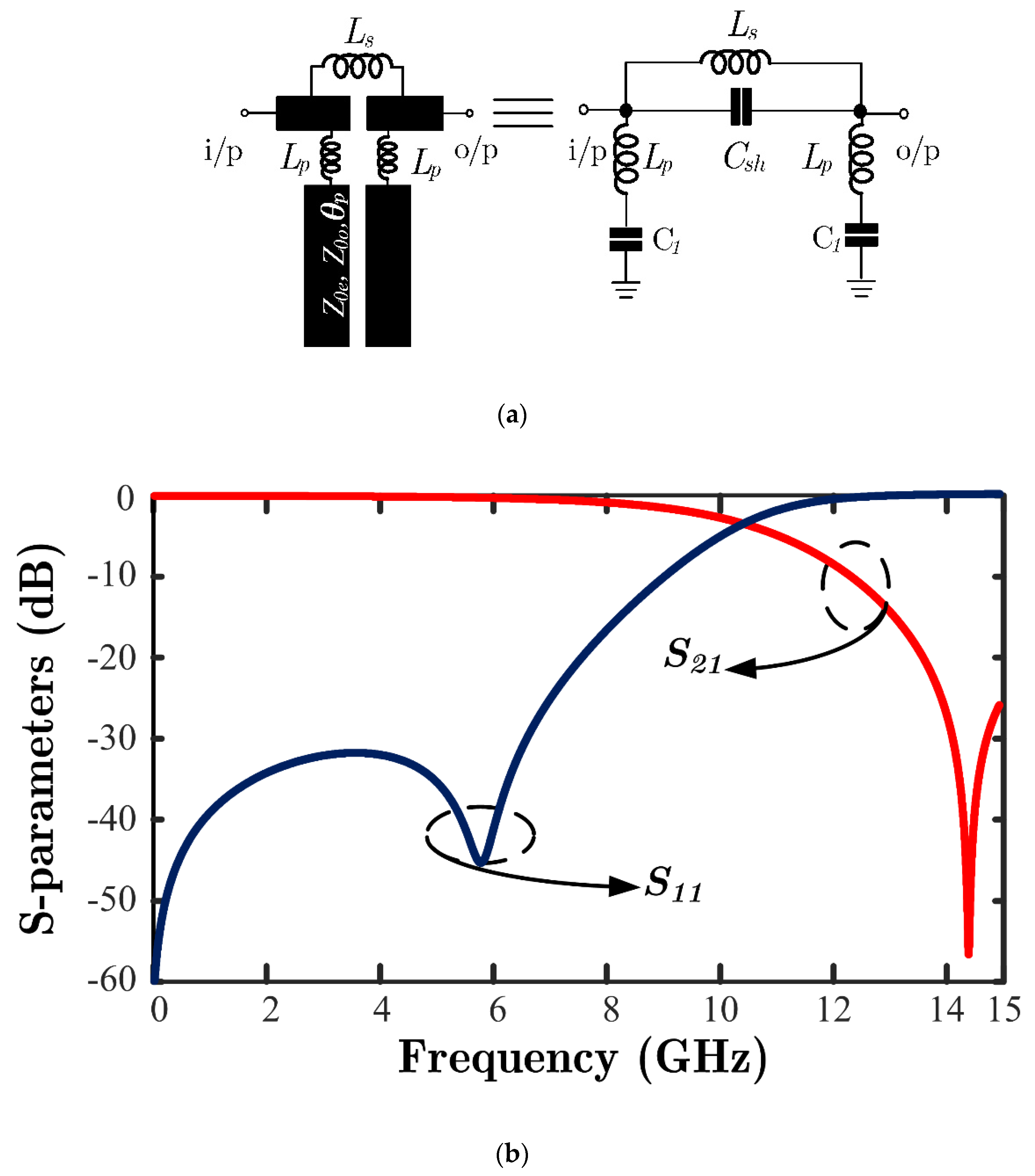
Figure 2a demonstrates the HPF design based on ICPCL. From Figure 1, ports 3 and 4 of the ICPCLs are connected to ground plane. This technique generates two inductors ( L 1 ) , as shown in Figure 2a. The remaining ports 1 and 2 act as input and output ports. The capacitor ( C S ) is connected in parallel between ports 1 and 2. The capacitor ( C s h ) is from fringing fields between the lines of the input and output ports. The operating frequency ( f 0 ) can be adjusted from the electrical angle of the PCL ( θ p ) , the compensated inductors ( L p ) , and the capacitor ( C S ) . In this HPF design, the cut-off frequency of 3.10 GHz is selected. Because of this cut-off frequency, the parallel-coupled lines in Figure 2a act as the inductors ( L 1 ) . Parameters for computer simulations can be obtained from Table 1. The scattering parameters of the HPF with the compensated inductors ( L p = 0.68 nH) and the cut-off frequency of 3.10 GHz, obtained from the computer simulation, is shown in Figure 2b. The transition band between the stopband and the passband is sharp as design. The results and the structure are applied for designing the proposed UWB-BPF using the ICPCLs.

2.3. Design of the LPF

Figure 3a presents the design of the LPF based on ICPCL. From Figure 1, ports 3 and 4 are not connected to ground plane. The remaining ports 1 and 2 are input and output ports. The inductor ( L s ) is connected between ports 1 and 2. The capacitor ( C s h ) is from the fringing fields between the lines of the input and output ports. The electrical angle of the PCL ( θ p ) , the compensated inductors ( L p ) , and the inductor ( L s ) are used to adjust the operating frequency ( f 0 ) . The cut-off frequency of 10.6 GHz is selected for this LPF design. With high cut-off frequency, the parallel-coupled lines in Figure 3a act as the capacitor ( C 1 ) . Table 1 shows the parameters for computer simulations. The frequency response of the LPF with the compensated inductors ( L p = 0.2 nH) and the cut-off frequency of 10.60 GHz, obtained from the computer simulation, is shown in Figure 3b. The scattering parameters present the properties of the LPF with the high slope of the transition band. The parameters of the LPF design are used in the design of the proposed UWB-BPF using the ICPCL.

2.4. Design of the Proposed UWB-BPF

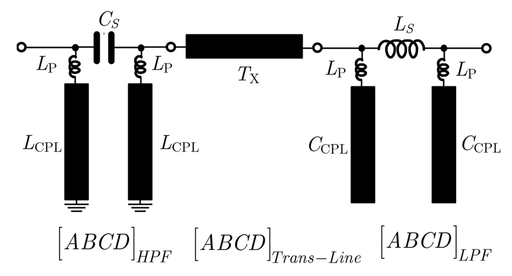
Based on the design and the simulated results of HPF and LPF in Figure 2b and Figure 3b, the HPF, the LPF, and the transmission line ( T x ) are connected, as shown in Figure 4, to form the proposed UWB-BPF. Figure 4 depicts the proposed UWB-BPF using the ICPCL. The input port of the HPF acts as an input port of the proposed UWB-BPF while the output port of the LPF functions as an output port of the proposed UWB-BPF. The center frequency ( f c ) is selected at 6.8 GHz. The lower cut-off frequency ( f c 1 ) and the upper cut-off frequency ( f c 2 ) are 3.10 and 10.60 GHz, respectively. Thus, the wide bandwidth is 7.5 GHz. The proposed UWB-BPF in Figure 4 is simulated with the parameters in Table 1. The substrate used in the computer simulations is AD260A from Rogers Corporation, Chandler, AZ ( ε r = 2.6 ,   h = 1   mm ,   and   t a n   δ = 0.0017 ). The HPF is constructed with the cut-off frequency ( f c 1 ) of 3.10 GHz while the LPF is designed with the cut-off frequency ( f c 2 ) of 10.60 GHz. The compensated inductors for the lower cut-off frequency ( f c 1 ) and the upper cut-off frequency ( f c 2 ) are 0.68 and 0.2 nH, respectively. The characteristic impedance of the PCL is 50 Ω, which has the even-mode characteristic impedance of 69.37 Ω and the odd-mode characteristic impedance of 36.03 Ω.
Simulations of all these parameters are performed and the simulated results are compared. Figure 5 shows the simulated results of transmission coefficients (S21) and reflection coefficients (S11) without compensated inductors. Figure 6 depicts the simulated results of transmission coefficients (S21) and reflection coefficients (S11) with compensated inductors.
The proposed UWB-BPF is designed with the center frequency ( f c ) of 6.80 GHz, lower cut-off frequency ( f c 1 ) of 3.10 GHz, upper cut-off frequency ( f c 2 ) of 10.60 GHz, and fractional bandwidth of 7.50 GHz. From the simulated results in Figure 5, the center frequency ( f c ) of the proposed UWB-BPF without compensated inductors is 6.90 GHz. The frequencies of the passband are from 3.10 GHz to 10.70 GHz. The fractional bandwidth of 7.60 GHz is obtained. From the simulated results with compensated inductors in Figure 6, the center frequency ( f c ) of the proposed UWB-BPF is 7.10 GHz. The lower cut-off frequency ( f c 1 ) and the upper cut-off frequency ( f c 2 ) are 2.91 and 11.30 GHz, respectively. The fractional bandwidth of 8.39 GHz is obtained from the simulated results. From the simulated results, we can confirm that the ICPCL can be effectively applied to the design of the UWB-BPF [1].

3. Experimental Results and Discussions

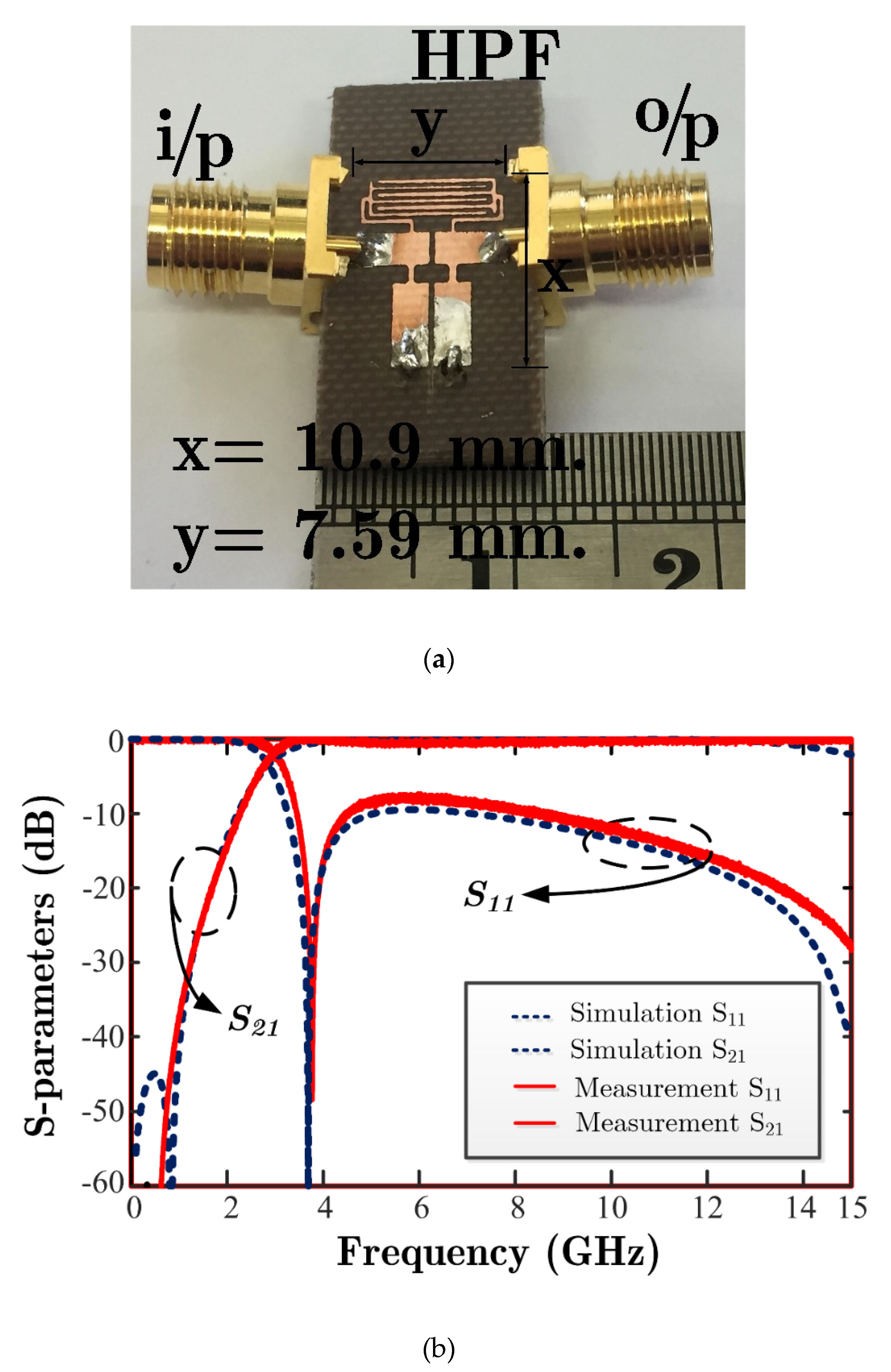
For performance assessment of the proposed filters, HPF, LPF, and UWB-BPF were fabricated on the AD260A substrate. The filters were designed and fabricated with the characteristic impedance of 50 Ω, even-mode characteristic impedance of 69.37 Ω, and odd-mode characteristic impedance of 36.03 Ω. From Figure 2a, the HPF was fabricated using the parameters in Table 2. The compensated inductors ( L p = 0.68   nH ) were generated with the transmission line. The capacitor ( C S ) was constructed with interdigital capacitors [24,25]. The cut-off frequency of the HPF was 3.10 GHz. W is the width of PCL, S is the gap length between PCLs, and L is the length of PCLs. Figure 7a demonstrates a photograph of the HPF. The simulated and experimental results of the HPF are depicted in Figure 7b. From Figure 7b, the cut-off frequencies of the simulated and experimental results are 2.88 and 2.87 GHz, respectively. The measured return loss and the measured insertion loss of the HPF at the center frequency of 6.8 GHz are better than −10 and −0.87 dB, respectively.
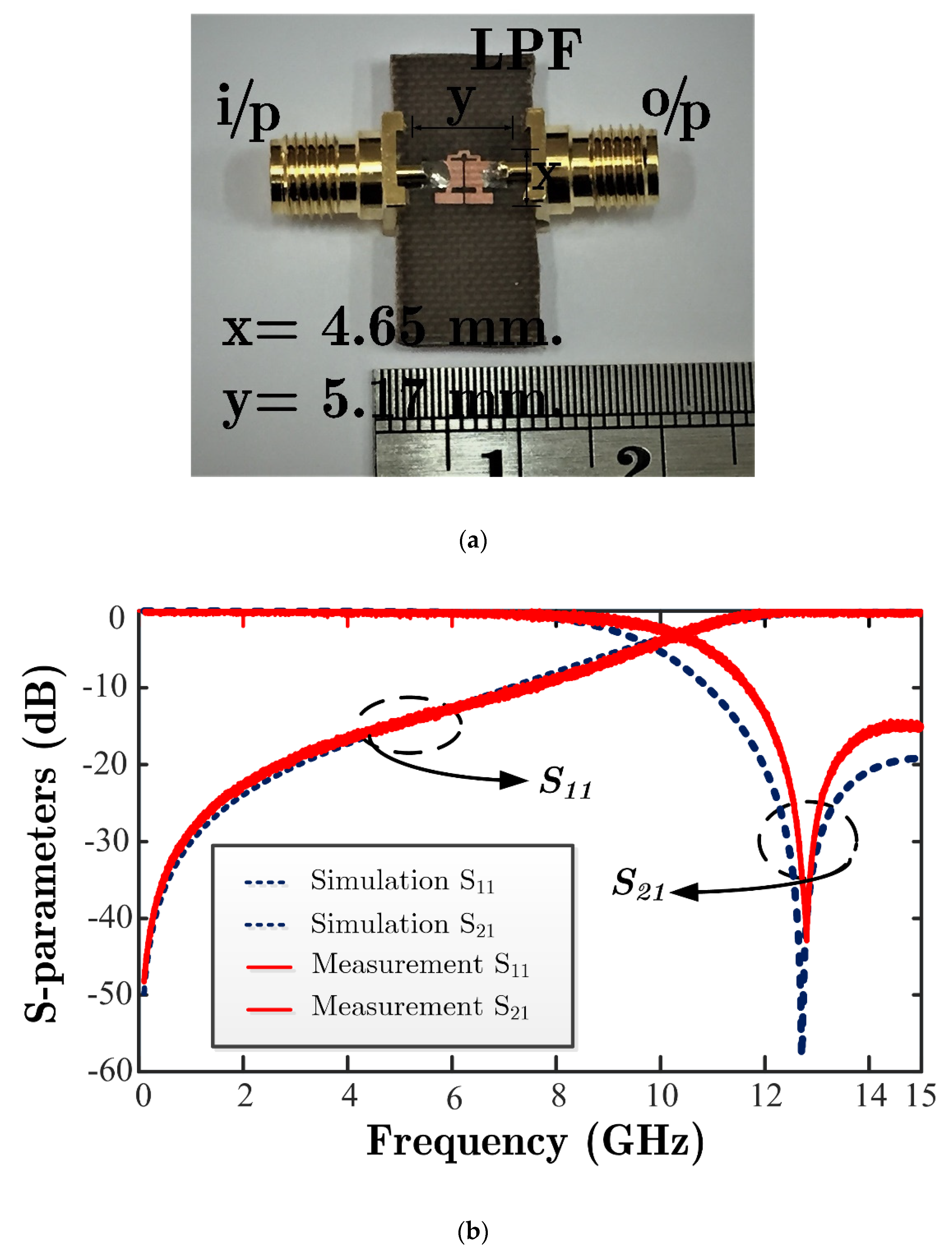
From Figure 3a, the LPF was constructed using the parameters in Table 2. The compensated inductors ( L p = 0.2   nH ) were generated with the transmission line. The cut-off frequency of the LPF was 10.60 GHz. Figure 8a shows a photograph of the LPF. The simulated and experimental results of the LPF are shown in Figure 8b. From Figure 8b, the cut-off frequencies of the simulated and experimental results are 9.70 and 10.56 GHz, respectively. At the center frequency of 6.80 GHz, the measured return loss of the LPF is better than −12 dB while the measured insertion loss of the LPF is −0.63 dB. From the measured results of the HPF and the LPF, the experimental cut-off frequencies are located near the simulated cut-off frequencies.
To construct the proposed UWB-BPF with ICPCL, the HPF, the LPF, and the transmission line were connected as shown in Figure 4. The UWB-BPF was fabricated using the combinations of parameters in Table 2. Figure 9a is a photograph of the fabricated UWB-BPF. The proposed UWB-BPF was measured to obtain the measured results using the N5230A PNA-L Network Analyzer. Figure 9b shows the simulated and measured results of the proposed UWB-BPF. It demonstrates very good agreement between the simulated and experimental results.
From the measured results, the proposed filter can attenuate unwanted frequencies (2f0) in the upper stopband and increase the skirt slope of transmission coefficients (S21) in the lower and upper transition bands. The lower cut-off frequency is 2.92 GHz, while the upper cut-off frequency is 10.95 GHz. The center frequency is located at the frequency of 6.94 GHz. Its passband operates in the range of 2.92–10.95 GHz. The fractional bandwidth of the proposed filter is 8.03 GHz (the fractional bandwidth of 107%). The measured return loss and insertion loss at the center frequency of 6.94 GHz are better than −12 and −0.49 dB, respectively. Moreover, the proposed UWB-BPF can eliminate the spurious frequencies at 2f0, which is greater than 30 dB.
Table 3 provides a comparison with other UWB techniques [26,27,28]. The previous studies are chosen from the requirements of the Federal Communications Commission. An intentional UWB device is specified as the device that has the bandwidth equal to or more than 20% of the center frequency or which has the bandwidth equal to or more than 0.5 GHz. Additionally, various UWB filter design techniques have been proposed to meet the required UWB frequency mask (3.1 to 10.6 GHz) [28]. In [26], the circular ring resonator was applied to the BPF. In [27], the coupled-line resonator was used to design the UWB filter. Additionally, in [28], lumped capacitors were added in the UWB filter. From Table 3, it is found that the proposed UWB-BPF provides the widest bandwidth (107%) compared to other techniques and there is the electrical length equation for the UWB design. The proposed UWB-BPF achieves the minimum insertion loss (−0.49 dB), the high return loss (−12 dB), and the compact circuit size compared to others.

4. Conclusions

In this paper, the fractional bandwidth of the proposed compact UWB-BPF that is wider than that of the Federal Communications Commission spectral mask is reported. The simple technique and the structure are presented to realize the proposed UWB-BPF using the HPF and the LPF connected in a series with the transmission line. The HPF and the LPF are independently generated from ICPCL. Simulated and measured results exhibit the outstanding UWB-BPF performance. The proposed UWB-BPF operates in the frequency range of 2.92–10.95 GHz. The fractional bandwidth of the proposed UWB-BPF is 8.03 GHz (107%). The experimental return loss at the center frequency of 6.94 GHz is better than −12 dB. The measured insertion loss is −0.49 dB at the center frequency. The proposed technique has been introduced for improving the skirt slope of the frequency response in the lower and upper transition bands and suppressing the unwanted frequencies at 2f0, which is more than 30 dB. The experimental results accord well with the simulated results. This can demonstrate the design concept of the proposed UWB-BPF.

Author Contributions

Conceptualization, M.J., N.A. and A.N.-O.; methodology, M.J. and N.A.; software, M.J. and N.A.; validation, M.J. and A.N.-O.; formal analysis, M.J., N.A. and A.N.-O.; investigation, M.J. and N.A.; resources, M.J. and A.N.-O.; data curation, M.J. and A.N.-O.; writing—original draft preparation, M.J., N.A. and A.N.-O.; writing—review and editing, N.A. and A.N.-O.; visualization, M.J. and A.N.-O.; supervision, N.A.; project administration, N.A.; funding acquisition, N.A. All authors have read and agreed to the published version of the manuscript.

Funding

This research project was financially supported by Mahasarakham University, Kantarawichai, Maha Sarakham, Thailand, grand number 5905021.

Data Availability Statement

The data that support the findings of this study are available upon reasonable request from the corresponding author.

Acknowledgments

The research was supported by the Research Unit for Computational Electromagnetics and Optical Systems (CEMOS), Faculty of Engineering, Mahasarakham University, Kantarawichai, Maha Sarakham, Thailand. The authors are grateful to acknowledge Ravee Phromloungsri for his useful advice.

Conflicts of Interest

The authors declare no conflict of interest.

References

  1. Sheng, H.; Orlik, P.; Haimovich, A.M.; Cimini, L.J.; Zhang, J. On the spectral and power requirements for ultra-wideband transmission. In Proceedings of the IEEE International Conference on Communications, Anchorage, AK, USA, 11–15 May 2003; pp. 738–742. [Google Scholar] [CrossRef]
  2. Meeloon, M.; Chaimool, S.; Akkaraekthalin, P. Broadband bandpass filters using slotted resonators fed by interdigital coupled lines for improving upper stopband performances. AEU-Int. J. Electron. Commun. 2009, 63, 454–463. [Google Scholar] [CrossRef]
  3. Sheleg, B.; Spielman, B.E. Broad-band directional couplers using microstrip with dielectric overlays. IEEE Trans. Microw. Theory Tech. 1974, 22, 1216–1220. [Google Scholar] [CrossRef]
  4. Hsu, C.; Hsu, F.; Kuo, J. Microstrip bandpass filters for ultra-wideband (UWB) wireless communications. In Proceedings of the IEEE MTT-S International Microwave Symposium Digest, Long Beach, CA, USA, 17 June 2005; pp. 679–682. [Google Scholar] [CrossRef]
  5. Cai, P.; Ma, Z.; Guan, X.; Yang, X.; Kobayashi, Y.; Anada, T.; Hagiwara, G. A compact UWB bandpass filter using two-section open-circuited stubs to realize transmission zeros. In Proceedings of the 2005 Asia-Pacific Microwave Conference Proceedings, Suzhou, China, 4–7 December 2005; pp. 1–4. [Google Scholar] [CrossRef]
  6. Yang, G.; Jin, R.; Geng, J.; Huang, X.; Xiao, G. Ultra-wideband bandpass filter with hybrid quasi-lumped elements and defected ground structure. IET Microw. Antennas Propag. 2007, 1, 733–736. [Google Scholar] [CrossRef]
  7. Longkul, A.; Angkawisittpan, A.; Suwannata, N. Design of a microstrip bandstop filter using folded spurline structures and its application. UBU Eng. J. 2012, 5, 48–55. Available online: https://ph02.tci-thaijo.org/index.php/eng_ubu/article/view/84348 (accessed on 20 September 2021).
  8. Bootthanu, N.; Angkawisittpan, N.; Chaimool, S. Development of wideband microstrip bandpass filters using DGS and stub. UTK Res. J. 2018, 12, 40–48. Available online: https://ph02.tci-thaijo.org/index.php/rmutk/article/view/142124 (accessed on 20 September 2021).
  9. Srisawat, S.; Angkawisittpan, N. A design of microstrip branch-line coupler with bandstop filter based on SITLs compensated parallel coupled lines. KKU Res. J. (GS) 2019, 19, 139–148. Available online: https://ph02.tci-thaijo.org/index.php/gskku/article/view/229439 (accessed on 20 September 2021).
  10. Aliqab, K.; Hong, J. Wideband differential-mode bandpass filters with stopband and common-mode suppression. IEEE Microw. Wirel. Compon. Lett. 2020, 30, 233–236. [Google Scholar] [CrossRef]
  11. Taibi, A.; Trabelsi, M.; Slimane, A.; Belaroussi, M.T.; Raskin, J. A novel design method for compact UWB bandpass filters. IEEE Microw. Wirel. Compon. Lett. 2015, 25, 4–6. [Google Scholar] [CrossRef]
  12. Wei, F.; Li, W.T.; Shi, X.W.; Huang, Q.L. Compact UWB bandpass filter with triple-notched bands using triple-mode stepped impedance resonator. IEEE Microw. Wirel. Compon. Lett. 2012, 22, 512–514. [Google Scholar] [CrossRef]
  13. Guvenli, K.; Yenikaya, S.; Secmen, M. Analysis, design, and actual fabrication of a hybrid microstrip-SIW bandpass filter based on cascaded hardware integration at X-band. Elektron. ir Elektrotechnika 2021, 27, 23–28. [Google Scholar] [CrossRef]
  14. Hong, J.; Lancaster, M.J. Microstrip Filters for RF/Microwave Applications; John Wiley & Sons: New York, NY, USA, 2001. [Google Scholar] [CrossRef]
  15. Gonzalez, G. Microwave Transistor Amplifiers: Analysis and Design; Pearson: London, UK, 1996; ISBN 0132543354. [Google Scholar]
  16. Chen, C. A coupled-line coupling structure for the design of quasi-elliptic bandpass filters. IEEE Trans. Microw. Theory Tech. 2018, 66, 1921–1925. [Google Scholar] [CrossRef]
  17. Phromloungsri, R.; Patisang, S.; Srisathit, K.; Chongcheawchamnan, M. A harmonic-suppression microwave bandpass filter based on an inductively compensated microstrip coupler. In Proceedings of the 2005 Asia-Pacific Microwave Conference Proceedings, Suzhou, China, 4–7 December 2005; pp. 1–4. [Google Scholar] [CrossRef]
  18. Kumpang, S.; Phromloungsri, R.; Chongcheawchamnan, M.; Krairiksh, M.; Robertson, I. Design and application of microstrip parallel-coupled lines employing step-impedance transmission-line compensation. IET Microw. Antennas Propag. 2009, 3, 410–415. [Google Scholar] [CrossRef]
  19. Phromloungsri, R.; Chongcheawchamnan, M.; Robertson, I. Inductively compensated parallel coupled microstrip lines and their applications. IEEE Trans. Microw. Theory Tech. 2006, 54, 3571–3582. [Google Scholar] [CrossRef]
  20. Sonasang, S.; Angkawisittpan, N. Design of microstrip parallel-coupled lines with high directivity using symmetric-centered inductors. Appl. Comput. Electromagn. Soc. J. 2021, 36, 657–663. [Google Scholar] [CrossRef]
  21. CST Studio Suite. Electromagnetic Field Simulation Software, Version 2021; Dassault Systèmes SE: Waltham, MA, USA, 2021. [Google Scholar]
  22. Phromloungsri, R.; Kumpang, S.; Chongcheawchamnan, M. Design high directivity parallel-coupled lines with step impedance transmission lines. In Proceedings of the 2008 Asia-Pacific Microwave Conference, Macau, China, 16–20 December 2008; pp. 1–4. [Google Scholar] [CrossRef]
  23. Thammawongsa, N.; Phromloungsri, R.; Jamsai, M.; Pornsuwancharoen, N. Design elliptic lowpass filter with inductively compensated parallel-coupled lines. Procedia Eng. 2012, 32, 550–555. [Google Scholar] [CrossRef] [Green Version]
  24. Angkawisittpan, N.; Manasri, T. Determination of sugar content in sugar solutions using interdigital capacitor sensor. Meas. Sri. Rev. 2012, 12, 8–13. [Google Scholar] [CrossRef]
  25. Obma, J.; Sa-ngiamvibool, W. The non-substrate interdigital capacitor level sensor. Przegląd Elektrotechniczny 2020, 96, 34–37. [Google Scholar] [CrossRef]
  26. Shome, P.; Khan, T. A compact design of circular ring-shaped MMR based bandpass filter for UWB applications. In Proceedings of the 2019 IEEE Asia-Pacific Microwave Conference (APMC), Singapore, 10–13 December 2019; pp. 962–964. [Google Scholar] [CrossRef]
  27. Djeddi, T.; Elsaadany, M.; Shams, S.; Hamouda, W. Compact ultra-wideband printed bandpass filter based on coupled-line resonator loading. In Proceedings of the 2018 18th International Symposium on Antenna Technology and Applied Electromagnetics (ANTEM), Waterloo, ON, Canada, 19–22 August 2018; pp. 1–2. [Google Scholar] [CrossRef]
  28. Ye, J.; He, L.; Zhong, X.; Qu, D. Design of ultra-wideband bandpass (UWB) filter with enhanced couplings by using lumped capacitors. In Proceedings of the 2018 International Conference on Microwave and Millimeter Wave Technology (ICMMT), Chengdu, China, 7–11 May 2018; pp. 1–3. [Google Scholar] [CrossRef]
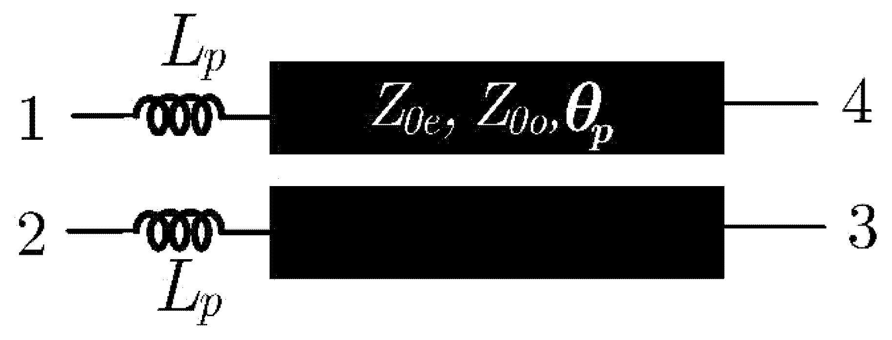
Figure 1. A sketch of the ICPCL.
Electronics 10 02575 g001
Figure 2. The design of the HPF: (a) The schematic of the HPF and (b) frequency response of the HPF with compensated inductors ( L p = 0.68   nH ) from computer simulations.
Electronics 10 02575 g002aElectronics 10 02575 g002b
Figure 3. The design of the LPF: (a) Schematic of the LPF and (b) the frequency response of the LPF with compensated inductors ( L p = 0.2   nH ) from computer simulations.
Electronics 10 02575 g003
Figure 4. The schematic of the proposed UWB-BPF.
Electronics 10 02575 g004
Figure 5. The results of the UWB-BPF without compensated inductors using computer simulations.
Electronics 10 02575 g005
Figure 6. The results of the UWB-BPF with compensated inductors using computer simulations.
Electronics 10 02575 g006
Figure 7. The prototype of the HPF: (a) A photograph of the HPF and (b) the simulated and measured results of the HPF with compensated inductors ( L p = 0.68 nH).
Electronics 10 02575 g007
Figure 8. The prototype of the LPF: (a) A photograph of the LPF and (b) the simulated and measured results of the LPF with compensated inductors ( L p = 0.2 nH).
Electronics 10 02575 g008
Figure 9. The prototype of the UWB-BPF: (a) A photograph of the proposed UWB-BPF and (b) the simulated and measured results of the proposed UWB-BPF.
Electronics 10 02575 g009
Table 1. Parameters for computer simulations.
SectionsElectrical ParametersComponentsDimensions of PCL
HPF Z 0 e = 69.37   Z 0 o = 36.03   ε e f f e = 2.25 ε e f f o = 1.83 L p = 0.0   nH C S = 0.8   pF W = 2.0   mm . S = 0.17   mm . L = 8.7   mm .
L p = 0.68   nH C S = 0.8   pF W = 2.0   mm S = 0.17   mm . L = 4.8   mm .
LPF Z 0 e = 69.37   Z 0 o = 36.03   ε e f f e = 2.31 ε e f f o = 1.87 L p = 0.0   nH L s = 0.3   nH W = 2.0   mm . S = 0.17   mm . L = 2.4   mm .
L p = 0.2   nH L s = 0.3   nH W = 2.0   mm . S = 0.17   mm . L = 0.8   mm .
Transmission Line Z 0 = 50   ε e f f   = 2.14 - W = 2.0   mm . L = 1   mm .
Table 2. Parameters for computer simulations with AD260A substrate.
SectionsElectrical
Parameters
  ( L P ) Dimensions
of PCLs
Components
HPF Z 0 e = 69.37   Z 0 o = 36.03   ε e f f e = 2.25 ε e f f o = 1.83 W = 0.4   mm . L = 1.2   mm . W = 2.0   mm . S = 0.17   mm . L = 4.8   mm . ( C S ) W = 0.2   mm . G = 0.2   mm . L = 6.0   mm . N P = 3
LPF Z 0 e = 69.37   Z 0 o = 36.03   ε e f f e = 2.31 ε e f f o = 1.87 W = 0.4   mm . L = 0.4   mm . W = 2.0   mm . S = 0.17   mm . L = 0.8   mm . ( L S ) W = 0.2   mm . L = 3.6   mm .
Transmission line Z 0 = 50   ε e f f   = 2.14 - W = 2.0   mm . L = 1   mm .
Table 3. Result comparison with other UWB techniques.
ReferencePassband (GHz)Bandwidth (GHz)Return Loss
(dB)
Insertion Loss (dB)Size (mm2)Electrical Length EquationTechniques
[26]3.05–10.627.57 (100.9%)−13−1.5122.40AvailableMultiple mode resonator
[27]2.50–7.004.50 (60%)−23No data9.94Not availableCoupled-line resonator
[28]3.00–10.207.20 (96%)−14.9−2263.25Not availableLumped capacitors
This work2.92–10.958.03 (107%)−12−0.49121.48AvailableICPCL
Publisher’s Note: MDPI stays neutral with regard to jurisdictional claims in published maps and institutional affiliations.