Article

A 6.89-MHz 143-nW MEMS Oscillator Based on a 118-dBΩ Tunable Gain and Duty-Cycle CMOS TIA

1
Department of Electrical and Computer Engineering, McGill University, Montréal, QC H3A 0G4, Canada
2
MEMS Vision International Inc., Montreal, QC H4P 2R9, Canada
3
Department of Electrical and Computer Engineering, University of Dayton, Dayton, OH 45469, USA
*
Author to whom correspondence should be addressed.
Electronics 2021, 10(21), 2646; https://doi.org/10.3390/electronics10212646
Submission received: 23 September 2021 / Revised: 24 October 2021 / Accepted: 25 October 2021 / Published: 29 October 2021
(This article belongs to the Section Microelectronics)

Abstract

:
This article presents a 6.89 MHz MEMS oscillator based on an ultra-low-power, low-noise, tunable gain/duty-cycle transimpedance amplifier (TIA) and a bulk Lamé-mode MEMS resonator that has a quality factor (Q) of 3.24 × 10⁶. Self-cascoding and current-starving techniques are used in the TIA design to minimize the power consumption and tune the duty-cycle of the output signal. The TIA was designed and fabricated in TSMC 65 nm CMOS process technology. Its open-loop performance has been measured separately. It achieves a tunable gain between 107.9 dBΩ and 118.1 dBΩ while dissipating only 143 nW from a 1 V supply. The duty-cycle of the output waveform can be tuned from 23.25% to 79.03%. The TIA has been interfaced and wire bonded in a series-resonant oscillator configuration with the MEMS resonator and mounted in a small cavity standard package. The closed-loop performance of the whole oscillator has been experimentally measured. It exhibits a phase noise of −128.1 dBc/Hz and −133.7 dBc/Hz at 1 kHz and 1 MHz offsets, respectively.

1. Introduction

Timing and frequency reference oscillators are pivotal blocks in almost all electronic systems. Emerging applications, including internet-of-things (IoT) and mobile devices, impose stringent requirements on power consumption (battery life), cost, and size [1]. In recent years, MEMS-based reference oscillators have become a key alternative to those based on quartz crystal resonators to enable miniaturized systems along with high performance levels [2,3,4]. Figure 1 shows the block diagram of a MEMS-based oscillator system, where a transimpedance amplifier (TIA) and a MEMS resonator are connected in a positive feedback loop. R M , C M , L M , C f , and C P are the MEMS resonator’s electrical model motional resitance, motional capacitance, motional inductance, feedthrough capacitance, and parasitic capacitance, respectively.
The loop sustains oscillation if the forward gain of the TIA overcomes the resonator series losses represented by R M . Typically, MEMS resonators are actuated by either piezoelectric or capacitive transduction mechanisms. Piezoelectrically transduced resonators have smaller R M (less losses) but require specialized fabrication technologies that are not available in many standard semiconductor foundries. Capacitively transduced resonators have a higher R M in the range of tens of kΩ but are more suited for monolithic CMOS integration [5], and these devices offer a high-quality factor (Q), small size, and good stability [6,7,8,9,10,11]. Capacitive MEMS resonators require a high gain TIA to compensate for the high R M . Further, a low phase shift near the oscillation frequency ( f o ) is needed to sustain oscillation. This results in the trade-off between the need for a high gain-bandwidth product and low power consumption.
In this work, a 6.89 MHz MEMS oscillator based on a high Q bulk Lamé-mode MEMS resonator and an ultra-low-power, low-noise TIA is presented. A design methodology to achieve low power consumption and low phase noise is proposed, demonstrating the efficacy of using a high (Q) resonator to reach an ultra-low power design for the CMOS sustaining circuitry. The novel use of the self-cascoding and current-starving techniques in the TIA design has been introduced to minimize the power consumption and tune the duty-cycle of the output signal. Duty-cycle tuning is an added feature that can be used by other applications that requires a tunable duty-cycle, including switched-capacitor filters [12] and pulse-width control [13]. The fully integrated and packaged oscillator solution at this frequency achieves a very competitive performance in terms of power consumption and phase noise. The entire mounted system in a small cavity standard package significantly reduces the system cost and form factor compared using an external quartz crystal as a reference resonator.
Section 2 discusses the MEMS-based oscillator, showing the resonator and the sustaining amplifier circuit used in forming the oscillator. It presents the proposed methodology, TIA circuit design, and noise analysis. Section 3 covers the performance and robustness of the proposed TIA circuit. Section 4 shows the experimental validation used to test the stand-alone TIA performance, the measurement results of the overall oscillator system, and provides a comparison with the state-of-the-art designs. Finally, Section 5 provides the conclusion of the presented work.

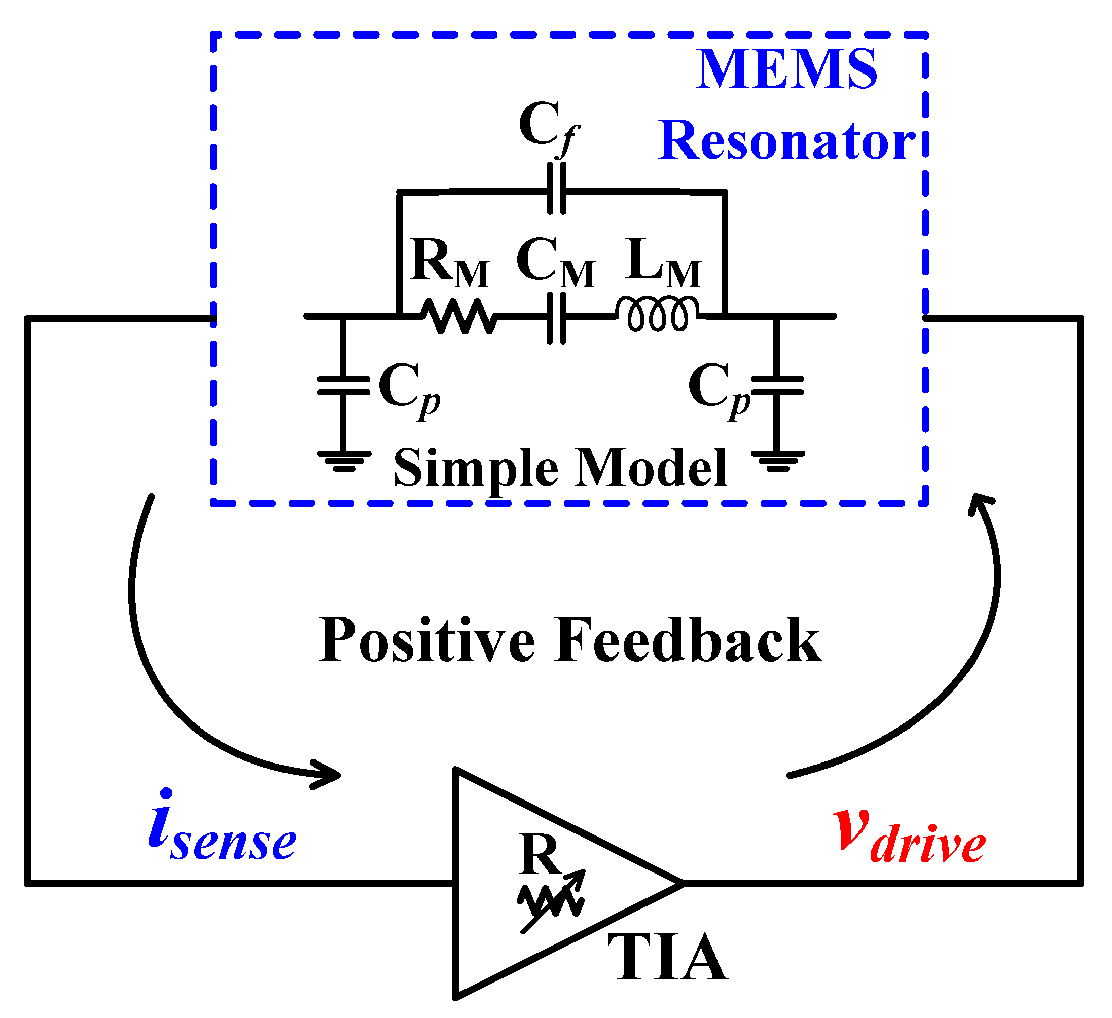
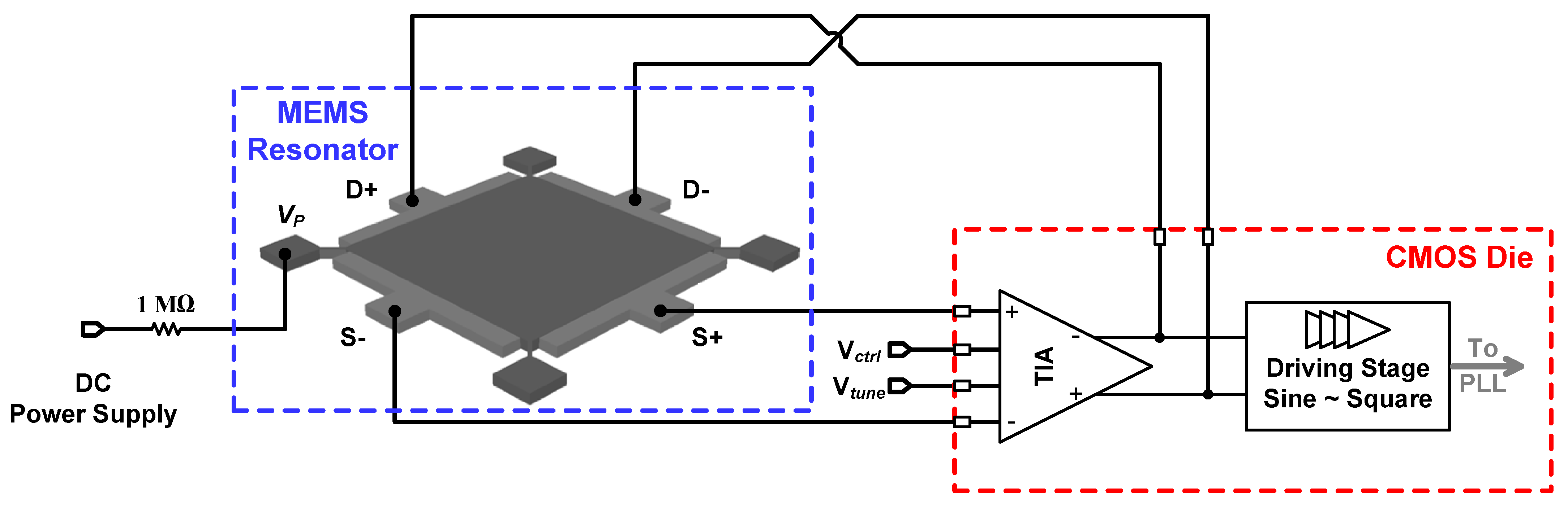
2. MEMS-Based Oscillator

Figure 2 shows the MEMS-based oscillator block diagram. The oscillator is based on a differential bulk square resonator connected in a positive feedback loop with the TIA. The oscillator is then to be connected to an integer-N PLL to synthesize a higher output frequency from the proposed input MEMS-based reference oscillator. The focus of the work here is the MEMS-based oscillator (not the PLL).

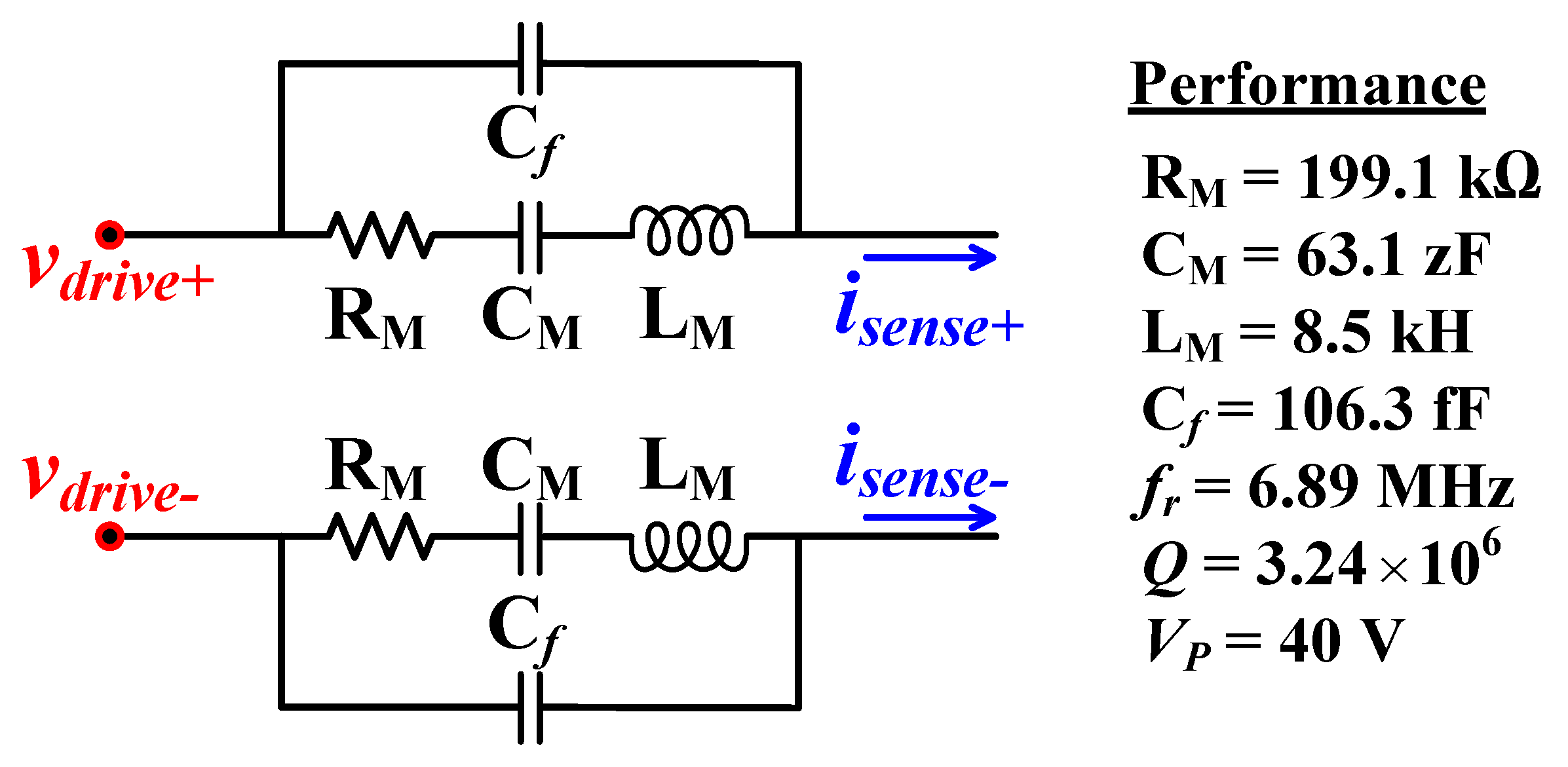
2.1. Bulk Lamé-Mode Square Resonator

The MEMS resonator used in this work is a bulk Lamé-mode wafer-level vacuum encapsulated at 10 mTorr. The resonator is fabricated using the MEMS Integrated Design for Inertial Sensors (MIDIS) technology, a pure-play commercial process provided by Teledyne DALSA Semiconductor Inc. It features low-leakage and vacuum level ultra-clean encapsulation. At a polarization voltage ( V P ) of 40 V, the measured resonance frequency ( f r ) is 6.8953 MHz, with a Q factor of 3.24 × 10⁶. This leads to a frequency-quality factor (f-Q) product of 2.23 × 10¹³ Hz. Figure 3 shows the measured frequency response of the resonator at a V P of 40 V.
Figure 4 shows the fitted linear RLC electrical equivalent model extracted by measuring the output of the resonator at 6.89 MHz while being biased at a V P of 40 V [14].

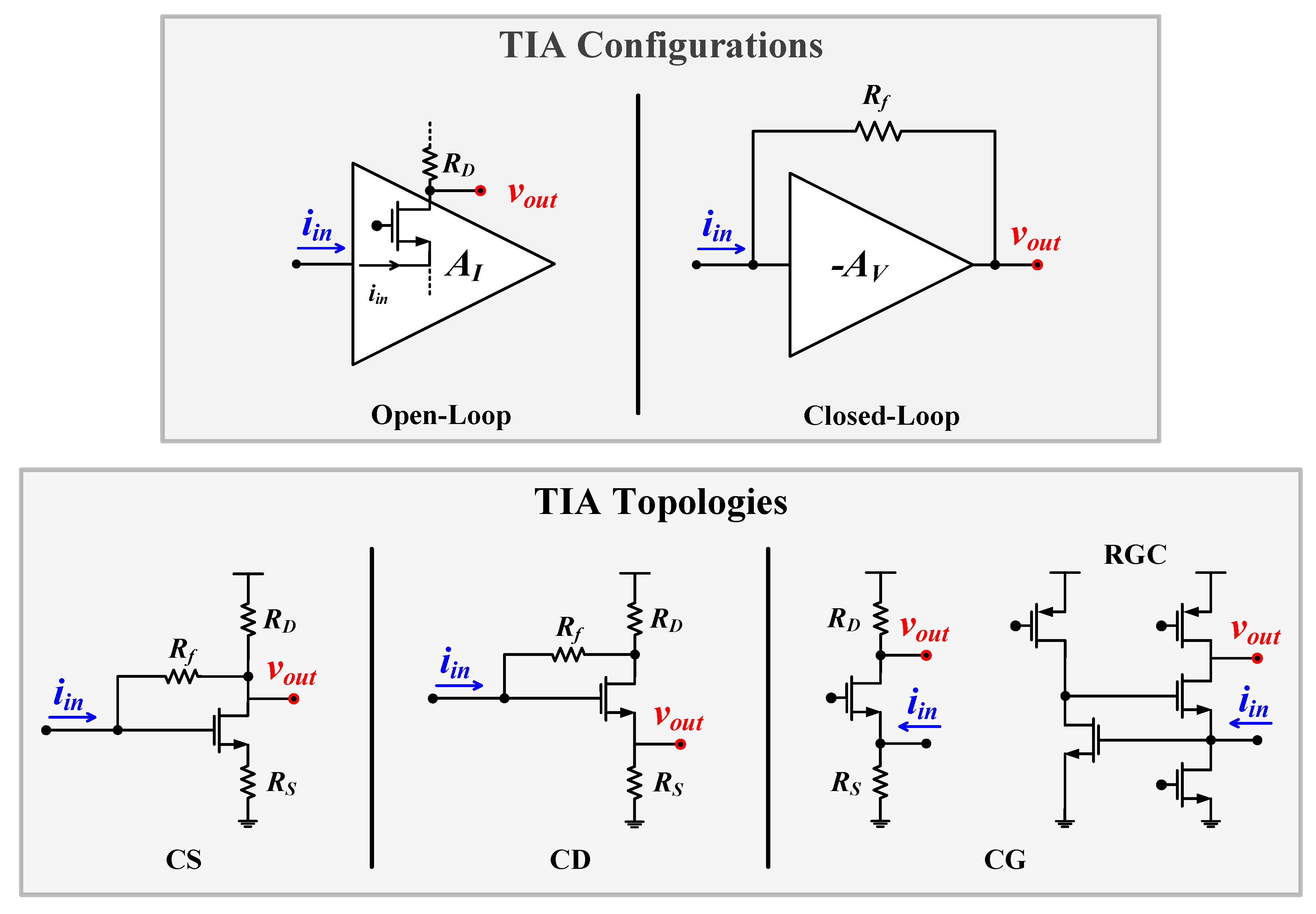
2.2. Sustaining Amplifier Configurations and Topologies

Figure 5 shows simple diagrams of different TIA configurations and topologies.There are two main general configurations used to realize a TIA: the open-loop configuration and the closed-loop (feedback) configuration. The open-loop TIA configuration is based on amplifying the input current using a current amplifier ( A I ), then converting it into an output voltage by passing the output current through a resistive load. Although open-loop TIAs may offer a lower power consumption than the closed-loop ones, they have a higher noise that cannot be tolerated for some applications [15]. On the other hand, the closed-loop configuration offers a lower noise and a more flexible gain–bandwidth (GBW) trade-off relationship. This makes it the most used for micromechanical oscillators. This configuration is based on a voltage amplifier ( A V ) with a negative shunt-shunt feedback from the output to the input. The shunt-shunt feedback lowers the system input and output impedances by the loop gain, which helps in increasing the TIA’s bandwidth. In addition, the amplifier’s input-referred noise is reduced by the square of the feedback resistor, bringing an extra advantage for low phase-noise MEMS-based oscillator applications.
Different topologies, including common-source (CS), common-gate (CG), and common-drain (CD), are used to realize the single stage or multistage amplifier. The CG topology, such as the regulated-cascode (RGC) amplifier, inherently, has low input impedance but suffers from a high input-referred noise. This makes the CG topology unsuitable for low-phase noise and low-power applications [16]. The CD topology offers a low output impedance but exhibits a poor linearity and a low dynamic range, resulting in higher phase-noise. The CS topology offers a larger output swing and can be operated from a lower supply, which further helps in reducing the power consumption. In addition, the dynamic range is improved due to the higher output swing resulting in a lower phase-noise floor. All these features make the closed-loop configuration, negative shunt-shunt feedback CS topology better suited for capacitive MEMS resonators and an optimum choice for our application.

2.3. Proposed Methodology and TIA Circuit

For an RLC circuit in a closed loop with a TIA, as shown in Figure 1, the total phase in the loop at the frequency of oscillation ( f o ) is, theoretically, zero. For a TIA phase shift ( φ ), where | t a n φ | Q , Equations (1) and (2) from [17] can be applied:
f o f r ( 1 + t a n φ 2 Q ) ,
where f r is the resonance frequency. A unity loop gain should be maintained at f o ; hence, a TIA gain ( R T I A ) is required as:
R T I A R M | c o s φ | .
Thus, for a very high Q MEMS resonator as the one used here, which has a Q of 3.24 × 10⁶, a phase shift of −80° changes f o by only 2 ppm. Equations (1) and (2) show that a tolerable phase shift can be used to save significant power, which would have otherwise been needed to obtain a large bandwidth while not taking the full advantage of the high Q of the resonator. Thus, as shown in Figure 6a, the proposed TIA uses three distinct features: (a) self-cascoding, (b) current-starving, and (c) long transistor channel length (L). Figure 6b shows the self-cascoding technique that is used for low-voltage operation. It reduces the channel length modulation effect while offering high output swing and DC gain [18].
The self-cascode structure consists of two transistors forming a composite transistor that mimics the same DC characteristics of a single long-channel transistor with a uniform width. It introduces two advantages over its DC-equivalent uniform-width single transistor: (a) a substantial area saving and (b) a higher cut-off frequency [19]. M2 in Figure 6b always operates in the triode region, while M1 can be operating either in the triode or the saturation regions. At the edge of saturation, the composite drain-source voltage ( V D S s a t c o m p o s i t e ) can be expressed as:
V D S s a t c o m p o s i t e = V D S s a t 1 + V D S 2 = V O V 1 + I D 2 R D S 2 ,
where V O V 1 is the overdrive voltage of M1. R D S 2 is the on resistance of M2 while operating in the triode region. This implies that the V D S 2 is very small and makes no discernible difference in the composite V D S s a t compared to that of its equivalent single transistor. This qualifies the self-cascode structure for low-power and low-voltage applications compared to regular-cascode structures that need a higher operating voltage [20,21]. The composite achieves a larger effective L—lower output conductance—by stacking smaller, shorter-length transistors. Assuming L 1 = L 2 and W 1 = m W 2 , the composite effective aspect ratio is expressed as:
W L | c o m p o s i t e = 1 m + 1 . W L | 1 = m m + 1 . W L | 2 .
From a layout perspective in advanced CMOS process technology nodes, most foundries strongly recommend in their process design kits (PDKs) building a long gate transistor length by stacking short gate transistors. This improves matching and the uniformity of the layout, which results in a more compact area by reducing the use of extra dummy layout cells used to ensure transistor layout uniformity post-fabrication. In addition, it is more precise in terms of the device model introduced by the PDK, as the device models may become inaccurate for very long gate lengths. The sum of the area footprints of M1 and M2 is smaller than that of the equivalent simple transistor. In addition, stacking reduces the leakage when the transistors are off. A stack of 2-transistors has 10× reduced leakage than that of an equivalent single transistor. This helps in reducing power dissipation. For equal chip areas, the voltage–gain ( A V ) relationship between the regular-cascode, the self-cascode, and a simple transistor is given by:
A V r e g u l a r c a s c o d e > A V s e l f c a s c o d e > A V s i m p l e t r a n s i s t o r .
although the regular cascode has a higher A V , this comes at the expense of a higher voltage drop (less headroom) and more power consumption.
The current starving technique controls the charging/discharging current flow to tune the duty-cycle, offering better noise performance [22,23], and reduces the power consumption. Finally, increasing the transistor channel length helps in reducing the output phase noise and the power consumption.

2.4. Noise Analysis

In MEMS oscillators, there are two main noise sources: (a) thermal noise from the resonator represented by 4 k B T / R M , where T is the absolute temperature and k B is the Boltzmann constant, and (b) the TIA’s input-referred current noise i n 2 ¯ . From [10,17,24], for a | t a n φ | Q and at low-frequency offsets ( Δ f ) , close to the carrier, the phase noise will be low as it is shaped by the resonator high Q, and it is given by:
L ( Δ f ) | R e s o n a t o r = 1 v d r i v e 2 K B T R M Q 2 f 2 Δ f 2 ,
the phase noise floor is proportional to R M 2 and i n 2 ¯ and can be expressed as:
L ( Δ f ) | F l o o r = 1 v d r i v e 2 i n 2 ¯ R M 2 Δ f ,
where v d r i v e is the resonator input driving voltage. Thus, it is important to minimize i n 2 ¯ . The shunt-shunt negative feedback reduces the amplifier’s input-referred noise power spectral density by the square of the feedback resistance and helps compensate for the direct proportionality of the noise floor to R M 2 . Neglecting the flicker noise, the thermal input-referred current noise for the design proposed here can be expressed as
i n 2 = 4 k B T [ ω 2 C i n 2 γ g m 1 + g m 4 + 1 R c t r l ] ,
where k B is the Boltzmann constant, T is the absolute temperature, ω is the angular frequency, C i n is the TIA total input capacitance, γ is a noise coefficient that depends on the transistor channel length (L), g m 1 and g m 4 are the transconductances of M1 and M4, respectively, and R c t r l is the shunt-shunt feedback resistor realized by transistor Mf.

3. System Performance and Robustness

3.1. Specifications and Performance
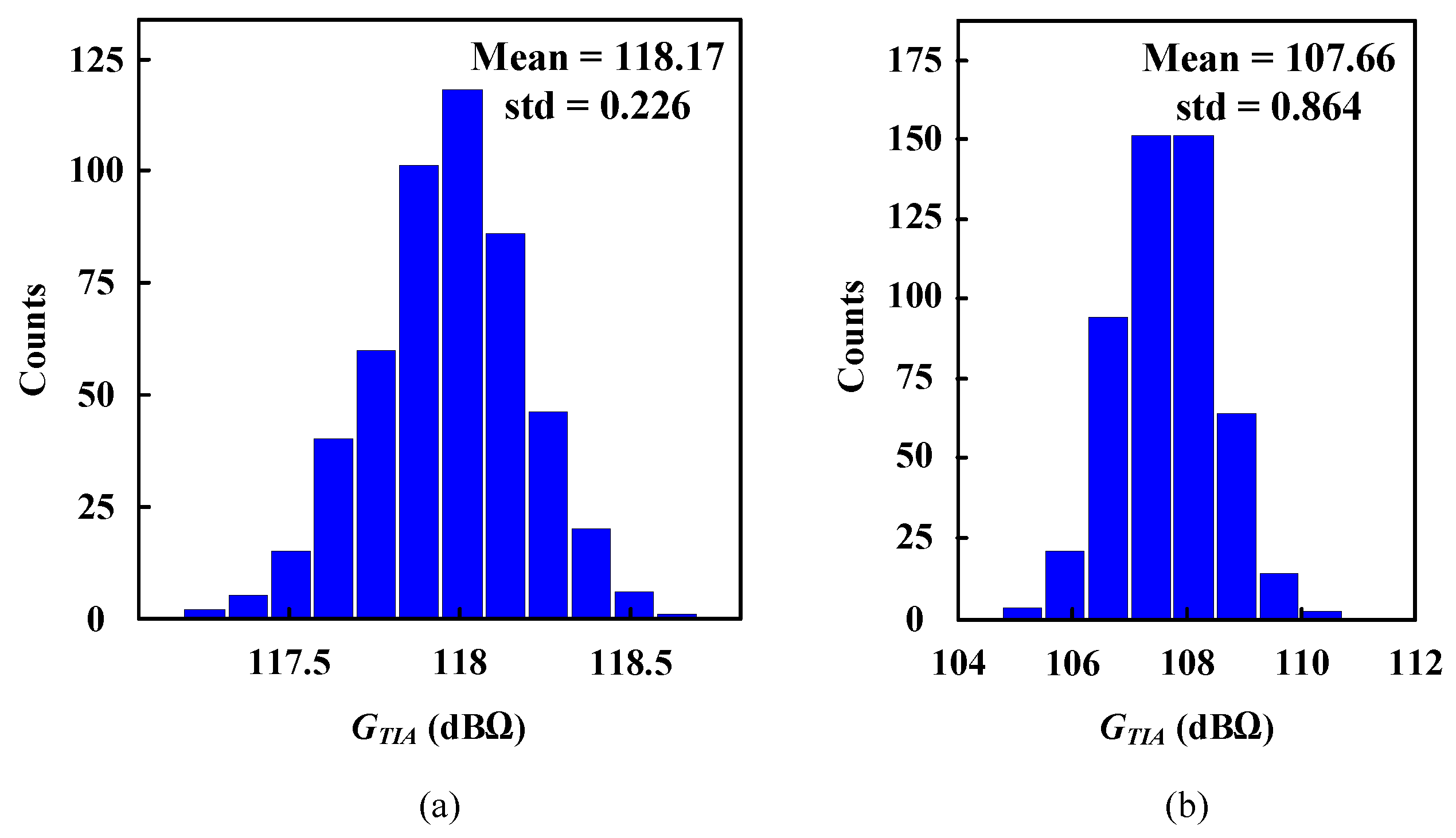
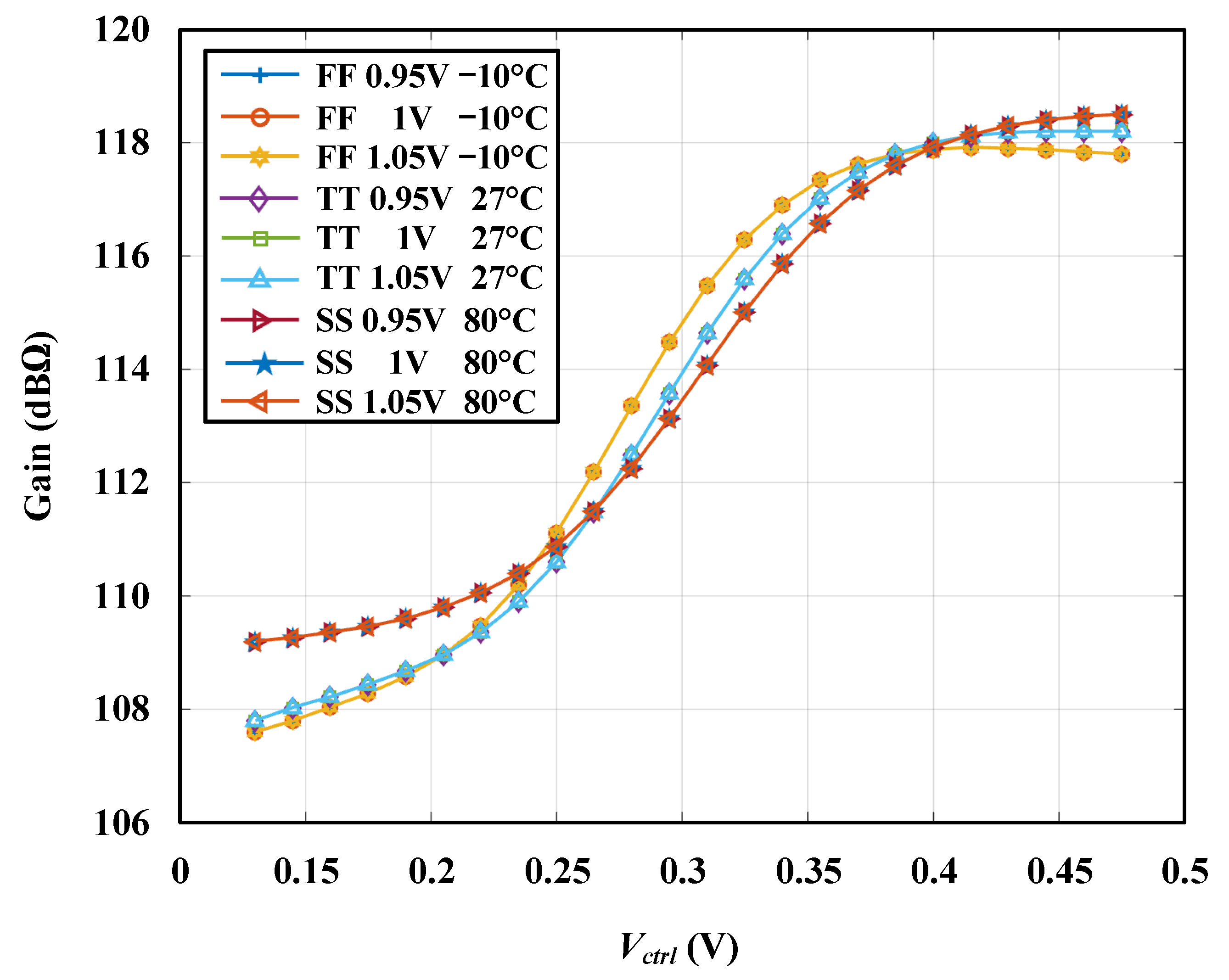
To sustain oscillations, an enough high gain is required to compensate for the MEMS resonator losses that are modeled with the resonator motional resistance ( R M ) in the electrical model. The used bulk Lamé-mode resonator has an R M of 199.1 kΩ, which corresponds to 105.97 dBΩ losses. The designed TIA should at least have a gain of 105.97 dBΩ to compensate for the resonator losses. Practically, at start-up, a higher gain may be needed to start the oscillation, where having a tunable gain feature becomes valuable.
The proposed TIA is developed in the TSMC 65 nm CMOS process technology. An open-loop simulation test is performed while loading the TIA with the MEMS resonator electrical model to check the TIA gain ( G T I A ) and performance. The designed TIA has a minimum gain of 107.6 dBΩ, which covers the minimum required gain to compensate for the resonator losses and any extra parasitic losses. The gain is tunable between 107.6 dBΩ and 118.2 dBΩ. The duty-cycle of the output waveform tested after the driving stage is tunable between 23.9% and 79.7%.

3.2. Robustness

To test the sensitivity of the proposed TIA circuit over transistor mismatches, a spectre post-layout conservative simulation was carried out on the circuit shown in Figure 6a using a Monte-Carlo analysis with a number of runs N = 500. Figure 7a shows the histogram of the TIA’s maximum gain: G T I A M a x = 118.2 dBΩ. It reports a mean of 118.17 dBΩ and a standard deviation (std) of 0.226 dBΩ. For the TIA’s minimum gain, G T I A M i n = 107.6 dBΩ, as shown by the histogram in Figure 7b, the mean and the std are 107.66 dBΩ and 0.864 dBΩ, respectively.
Figure 8 shows the post-layout TIA gain over three process corners (FF, TT, SS), supply variation range (1 V ± 0.05 V), and temperature between (−10 °C→ 80 °C) to test the design robustness over the process, voltage, and temperature (PVT) variations. The graph indicates a maximum gain tuning range of 10.6 dBΩ under the TT corner and a minimum gain tuning range of 9.3 dBΩ under the SS corner.

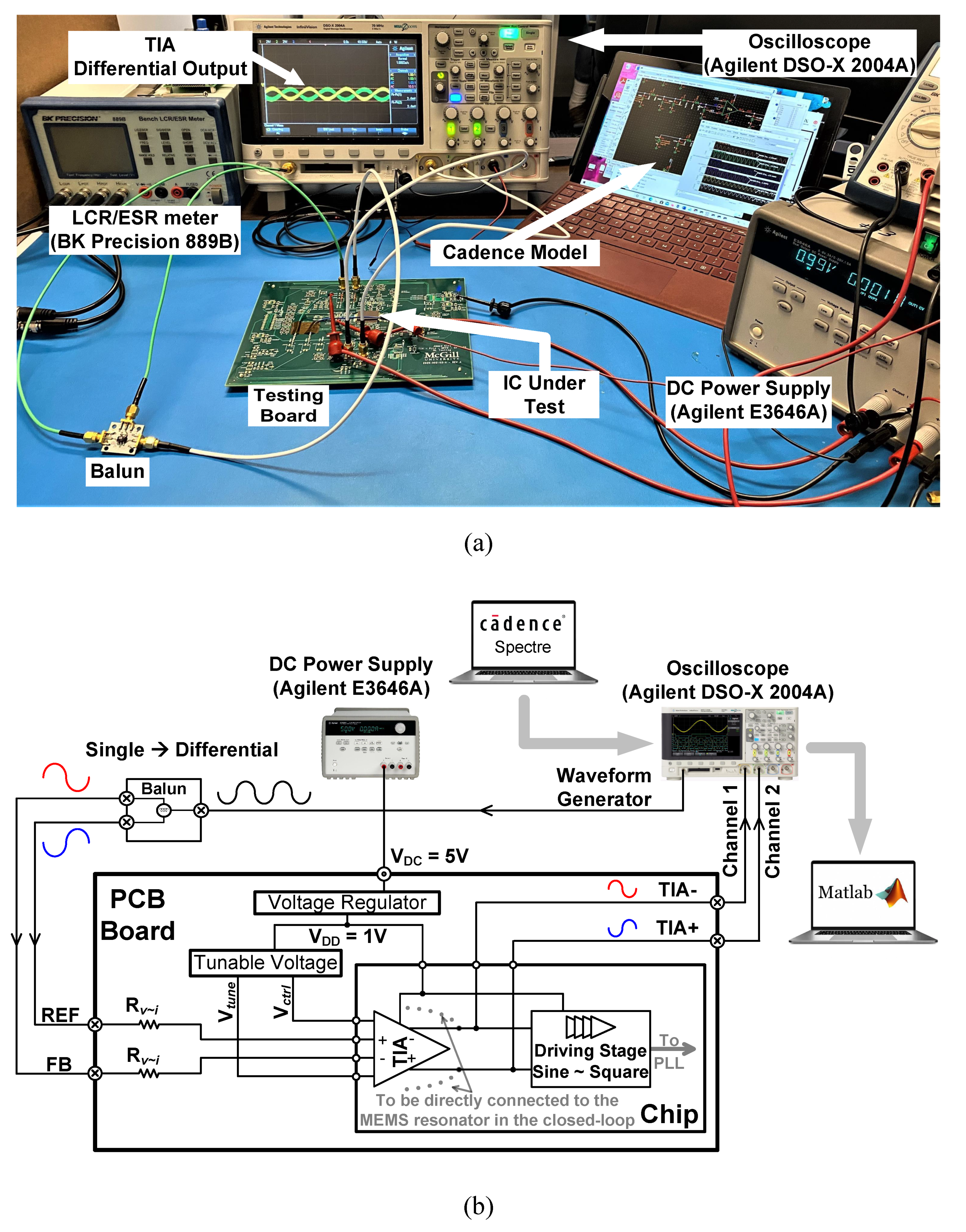
4. Experimental Results

To validate the fabricated design, the CMOS circuits have been tested in an open-loop configuration while considering all parasitic loads to validate the TIA open-loop performance. Then, a closed-loop testing has been performed after wire bonding the CMOS circuits to the MEMS resonator to test the closed-loop feedback oscillator performance. Five CMOS dies have been tested in total, and all the results are within 0.3% of the TT corner performance, which is in a good agreement with our Monte Carlo simulations.

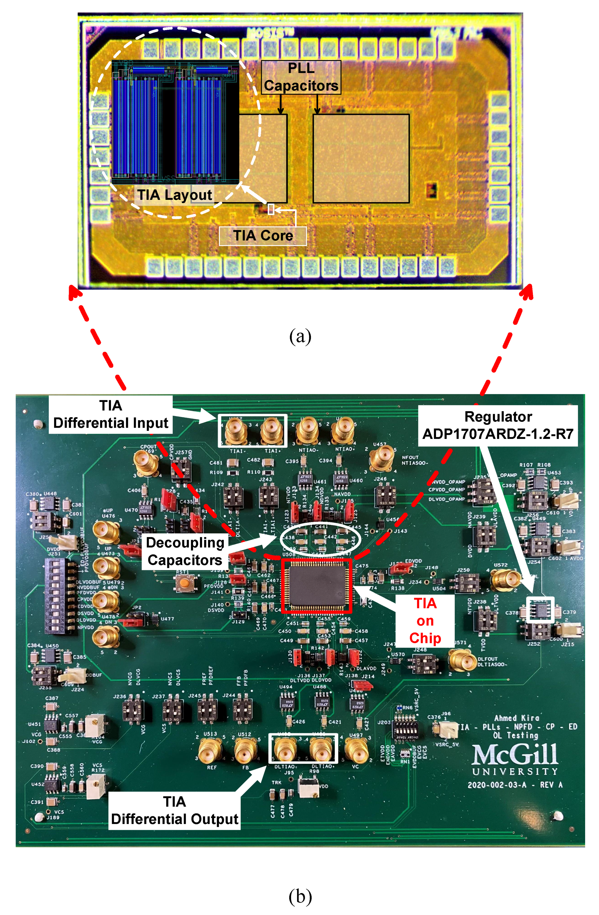
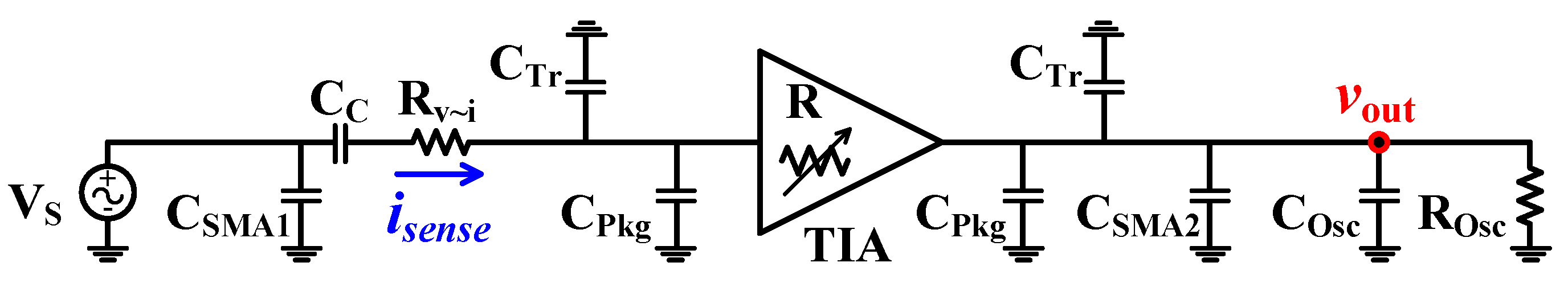
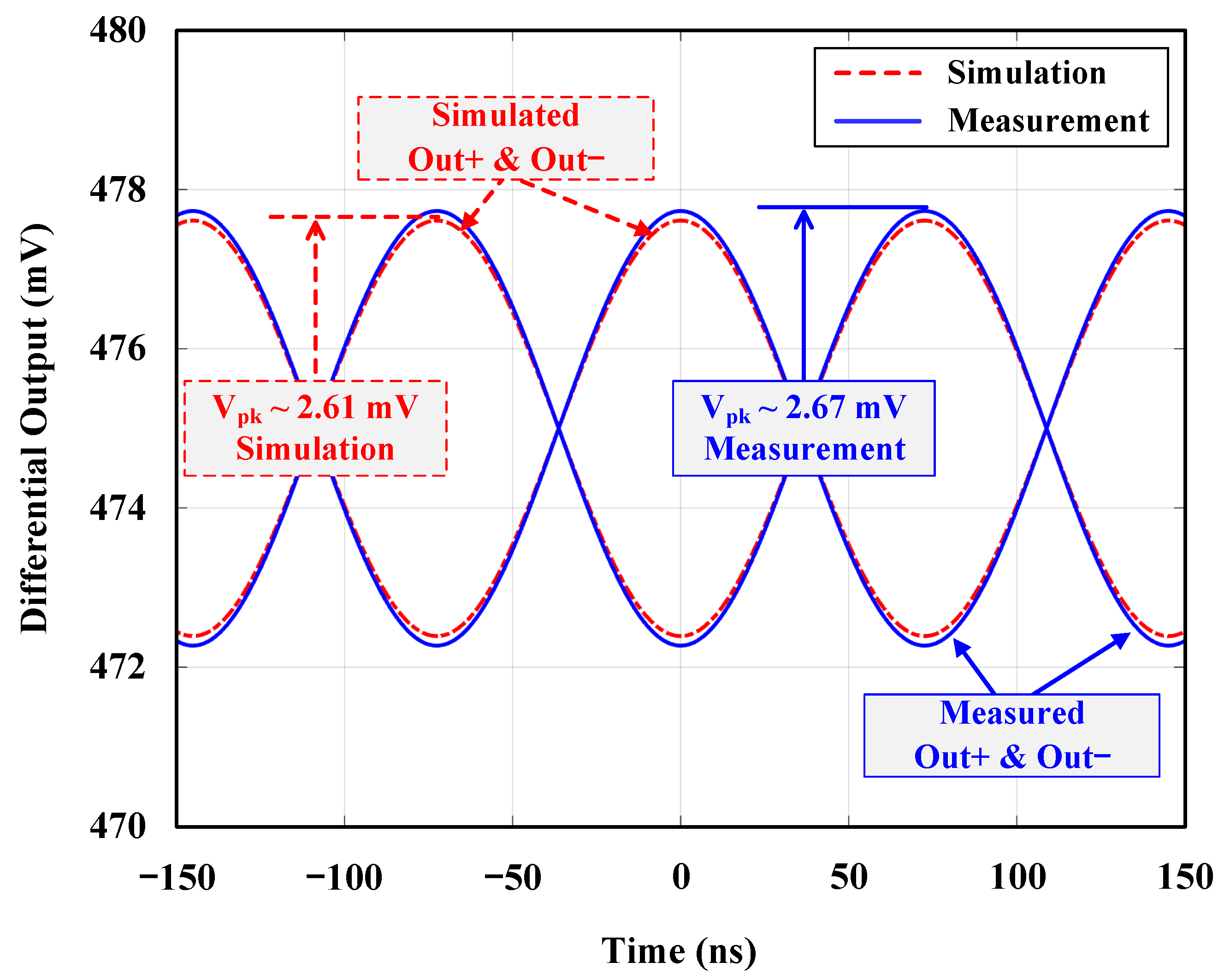
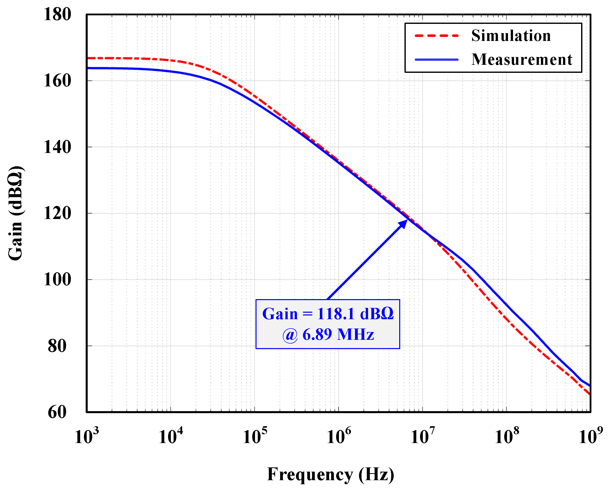
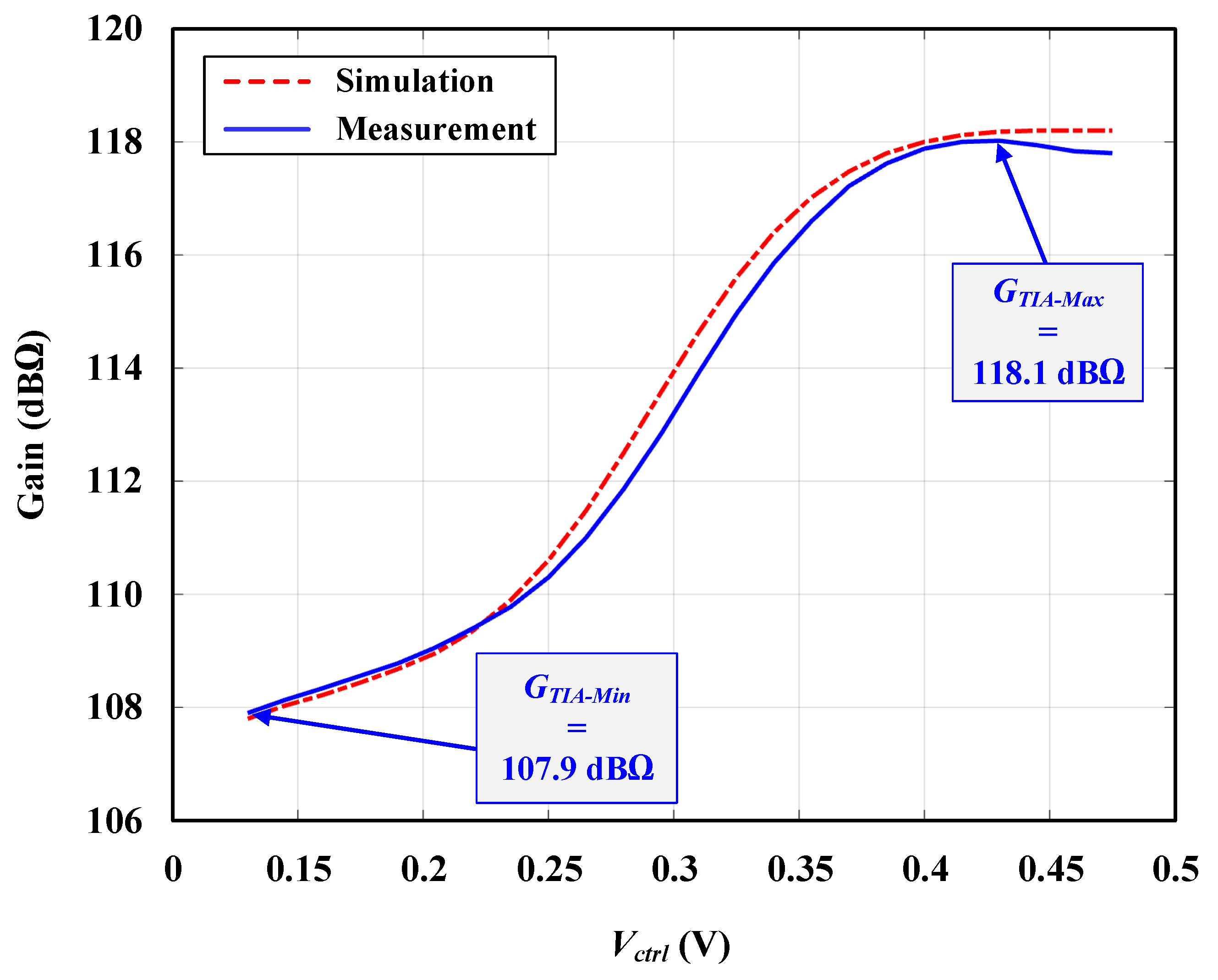
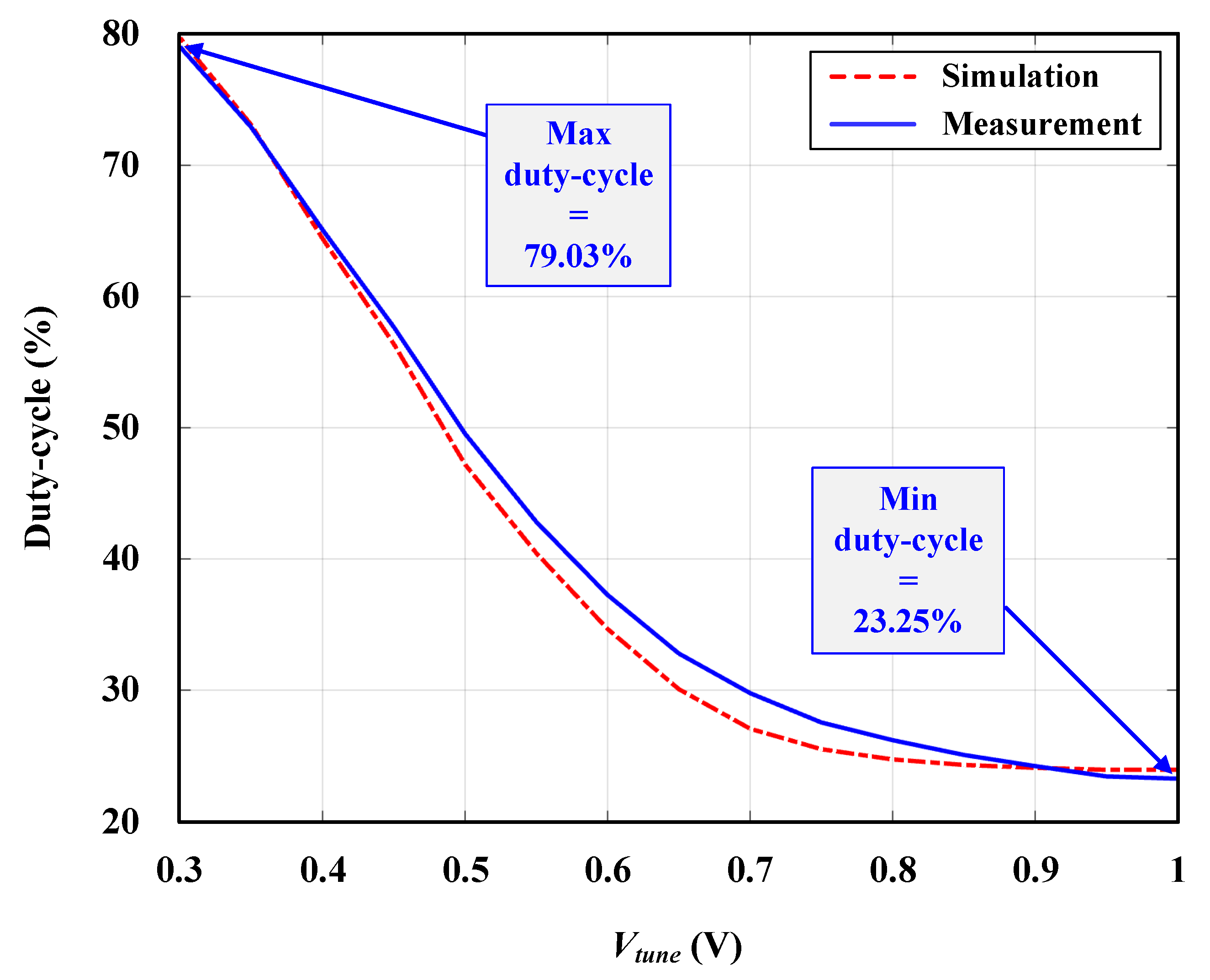
4.1. Open-Loop Validation

The stand-alone performance of the proposed TIA has been tested separately, without the MEMS resonator. Figure 9a shows the micrograph of the fabricated die highlighting the TIA block. The total active TIA CMOS area is 150.29 μm2 (12.38 μm × 12.14 μm).
The prototype CMOS die is assembled in an 80-pin ceramic quad flat pack (CQFP) package and mounted on a custom 4-layer printed circuit board (PCB), as shown in Figure 9b. The test board includes SMA connectors for the input/output signals, coupling capacitors (1 uF) at the input signals to filter out the DC component, and a voltage regulator (Analog Devices ADP1707ARDZ-1.2-R7) to regulate the input supply from a DC power supply source (Agilent E3646A). In addition, all power nets are decoupled with a network of decoupling capacitors (10 nF, 100 nF, 1 μF) connected in parallel and in an ascending order from the integrated circuit (IC) package lead. There are other components on the PCB—Figure 9b—that are not related to this specific TIA test.
A measurement setup has been built to test the TIA in an open-loop configuration without being connected to the MEMS resonator. First, we have built a post-layout simulation environment on Cadence that only includes the TIA in an open-loop configuration. Second, we modeled all the loading and the parasitic effects added by the measurement equipment and the PCB in the simulation environment to fairly compare the simulation results with the measurements. This validates the TIA performance and assures proper functionality when bonded to the MEMS resonator in a closed-loop feedback configuration.
To mimic the MEMS resonator, an excitation voltage at a frequency of 6.89 MHz was used, and a resistor (Rv∼i) was placed in series with the TIA input to convert this excitation voltage to a current in the range of the MEMS resonator sensed current. Figure 10 depicts the testing method, including all sources of parasitics.
The test has been applied in both the Cadence simulation environment and the measurement setup. Figure 11 shows the matching of the transient differential outputs obtained from both the simulation and the measurement.
The amount of parasitics seen by the TIA on the PCB while being connected to the measurement equipment is very large compared to when being only connected directly to the MEMS resonator. When the TIA is connected to the MEMS resonator in a closed feedback loop—which is the case in the end application—it is only loaded by less than 0.5 pF parasitic capacitance. On the other hand, in this PCB measurement setup, as will be shown shortly, the total parasitic capacitances loading the TIA output and input are 74.85 pF and 105.4 pF, respectively. Adding these loads in the Cadence simulation model will decrease the output signal amplitude by a considerable amount. This is expected as the TIA is designed to interface directly with the MEMS resonator where the level of parasitics is greatly reduced. By replicating the PCB parasitics in our Cadence model simulations, we can directly compare the results to see if the TIA is performing as expected. Table 1 shows the list of loads and parasitic effects.
The capacitances of the used SMA connector cables (CSMA1, CSMA2) have been measured using a bench LCR/ESR meter (BK Precision 889B). The PCB traces capacitances and the CQFP package lead capacitance have been estimated based on [25] and [26], respectively. The oscilloscope loading resistance (ROsc) and capacitance (COsc) were found in the oscilloscope (Agilent InfiniiVision DSO-X 2004A) manual [27]. After de-embedding the loading effects of the parasitics, the TIA performance has been captured. Figure 12 shows the measured transimpedance gain of the TIA. It reports the maximum gain at the resonance frequency ( f r ). The corresponding phase shift is −75.41°, which is the maximum phase shift that can occur. It is within the acceptable range, as discussed and shown earlier using Equations (1) and (2). For a lower gain, the phase shift will decrease.
It is worth noting that, in this work, the main objective all along has been to minimize power consumption while delivering an acceptable noise performance. The goal was not to solely minimize noise.
After an oscillator starts up, Equation (1) determines the noise performance. The effect of the phase shift, namely how far it occurs away from the resonator peak, is directly reflected in the phase noise performance. What permits the design to achieve very low power consumption is the very high Q-factor of the resonator used.
If we were to solely target noise minimization with this high Q-factor MEMS resonator instead of minimizing power, we could have achieved a much better noise performance than what we report here, but this obviously would have come at the expense of more power consumption and may have affected the overall figure of merit ( F o M ) achieved. This is a classic example of design parameters “balancing” based on the resources at hand and on the ultimate target objectives of the work: minimize power consumption while delivering a competitive F o M .
The measured tunable TIA gain with V c t r l is shown in Figure 13. It can be tuned between 107.9 dBΩ and 118.1 dBΩ. Figure 14 shows that the duty-cycle is tunable between 23.25% and 79.03%. All results are in a good agreement with the simulations. The actual measurement setup and its block diagram are depicted in Figure 15.

4.2. Closed-Loop Validation

The loop is closed to measure the oscillator’s performance after de-embedding the loading effects. The two die—MEMS and CMOS—are wire bonded together and packaged in an 80-pin quad flat no-lead (QFN) package. The QFN package has been chosen instead of the QFP due to the lower loading capacitance of its leads [26,28]. The package is mounted on a new custom PCB. All power nets are decoupled with a network of decoupling capacitors (10 nF, 100 nF, 1 μF) connected in parallel and in an ascending order from the IC package lead. A resistor of 1 MΩ has been connected in series between the MEMS V P and the DC power supply source (BK PRECISION 9110) to limit the maximum current on the polarization terminal in the case of an accidental pull-in between the electrodes of the MEMS device. Another DC power supply source (Agilent E3646A) was used to supply the CMOS circuits with a 1 V supply voltage. The ( V P ) has been raised up gradually, reaching a stable output at V P = 40 V. Oscillation start-up was ensured by design: The nominal gain of the TIA was set to be higher than the absolute minimum theoretical value in order to account for all process corners and potential PVT variations. The natural nonlinearities of the TIA/resonator act as intrinsic gain control. The provision of an additional/backup manual gain control could be used to reduce the gain to emulate an AGC whenever that was needed. Figure 16 shows the phase noise of the oscillator’s output. It reports a phase noise (PN) of −128.1 dBc/Hz and −133.7 dBc/Hz at 1 kHz and 1 MHz offsets, respectively. The TIA total power consumption ( P D C ) is 143 nW from a 1 V supply. Figure 17 shows the testing PCB and the wire bonded dies in the mounted package.

4.3. Figure of Merit

Table 2 compares this work with previously published state-of-the-art. To fairly compare different oscillators with different resonator R M and f o values, the figure of merit ( F o M ), as proposed by Seth et al. [17], was used:
F o M = 1 L ( Δ f f o ) k B T P D C R M 2 f o 2 ,
where L ( Δ f f o ) is the phase noise 1 MHz offset, and P D C is the DC power consumption in Watt.
It considers several points including: (a) for a very high Q, the 1 / f 2 and 1 / f 3 regions occur at low-frequency offsets. Thus, the PN at 1MHz offset dominates and becomes the primary performance metric in these reference oscillators. (b) The DC power consumption, and hence, the PN should be normalized to it. (c) The PN at 1MHz offset of a reference oscillator in a PLL is scaled by the square of the division ratio; thus, the reference oscillator’s PN should be scaled to the inverse square of the reference frequency ( 1 / f o 2 ). (d) The PN at 1MHz offset also scales with the square of the resonator motional resistance R M , which is not part of the TIA circuit design, so the PN should be scaled as well by 1 / R M 2 .
This F o M is used in Table 2 to compare this work with previously published state-of-the-art. This work reports the highest F o M compared to other works reported in the literature.

5. Conclusions

In this paper, we have successfully implemented an extremely low-power, tunable gain/duty-cycle TIA. The TIA was integrated with a very high-quality factor (Q) bulk Lamé-mode MEMS resonator to implement an oscillator with competitive performance in terms of power consumption and phase noise. The TIA structure is based on the self-cascoding technique. The TIA has been fabricated in a TSMC 65 nm CMOS process. Experimental validations, open-loop and closed-loop, have been carried out to test the TIA performance. The TIA has a tunable gain from 107.9 dBΩ to 118.1 dBΩ and a tunable duty-cycle between 23.25% and 79.03% while consuming only 143 nW from a 1 V supply. The proposed design enables the TIA to be easily transferred and adopted into new, advanced CMOS technologies with lower supply conditions, thanks to the self-cascoding technique used. The oscillator reaches a phase noise of −128.1 dBc/Hz and −133.7 dBc/Hz at 1 kHz and 1 MHz offsets, respectively.

Author Contributions

All authors participated in the conceptualization and methodology of this work. Data curation, A.K., M.Y.E. and K.A.; writing—original draft preparation, A.K., M.Y.E. and K.A.; writing—review and editing, V.P.C. and M.N.E.-G.; supervision, V.P.C. and M.N.E.-G. All authors have read and agreed to the published version of the manuscript.

Funding

This research received no external funding.

Conflicts of Interest

The authors declare no conflict of interest.

References

  1. Nguyen, C.T.C. MEMS Technology for Timing and Frequency Control. IEEE Trans. Ultrason. Ferroelectr. Freq. Control 2007, 54, 251–270. [Google Scholar] [CrossRef] [PubMed] [Green Version]
  2. Bouchami, A.; Elsayed, M.Y.; Nabki, F. A 1.4-mW 14-MHz MEMS Oscillator Based on a Differential Adjustable-Bandwidth Transimpedance Amplifier and Piezoelectric Disk Resonator. IEEE Trans. Circuits Syst. I Regul. Pap. 2018, 65, 3414–3423. [Google Scholar] [CrossRef]
  3. Nabki, F.; Allidina, K.; Ahmad, F.; Cicek, P.; El-Gamal, M.N. A Highly Integrated 1.8 GHz Frequency Synthesizer Based on a MEMS Resonator. IEEE J. Solid-State Circuits 2009, 44, 2154–2168. [Google Scholar] [CrossRef]
  4. Li, M.; Li, C.; Hou, L.; Liu, Y.; Li, S. A 1.57mW 99dBΩ CMOS transimpedance amplifier for VHF micromechanical reference oscillators. In Proceedings of the 2012 IEEE International Symposium on Circuits and Systems (ISCAS), Seoul, Korea, 20–23 May2012; pp. 209–212. [CrossRef]
  5. Nabki, F.; El-Gamal, M.N. A high gain-bandwidth product transimpedance amplifier for MEMS-based oscillators. In Proceedings of the ESSCIRC 2008—34th European Solid-State Circuits Conference, Edinburgh, UK, 15–19 September 2008; pp. 454–457. [Google Scholar] [CrossRef]
  6. Alsolami, A.; Zaman, A.; Rivera, I.F.; Baghelani, M.; Wang, J. Improvement of Deep Reactive Ion Etching Process For Motional Resistance Reduction of Capacitively Transduced Vibrating Resonators. IEEE Sens. Lett. 2018, 2, 1–4. [Google Scholar] [CrossRef]
  7. Rocheleau, T.O.; Naing, T.L.; Nguyen, C.T.C. Long-Term Stability of a Hermetically Packaged MEMS Disk Oscillator. In Proceedings of the 2013 Joint European Frequency and Time Forum International Frequency Control Symposium (EFTF/IFC), Prague, Czech Republic, 21–25 July 2013; pp. 209–212. [Google Scholar] [CrossRef]
  8. Pourkamali, S.; Hashimura, A.; Abdolvand, R.; Ho, G.; Erbil, A.; Ayazi, F. High-Q Single Crystal Silicon HARPSS Capacitive Beam Resonators With Self-Aligned Sub-100-nm Transduction Gaps. Microelectromech. Syst. J. 2003, 12, 487–496. [Google Scholar] [CrossRef] [Green Version]
  9. Clark, J.; Hsu, W.T.; Abdelmoneum, M.; Nguyen, C.C. High-QUHF Micromechanical Radial-ContourMode Disk Resonators. J. Microelectromech. Syst. 2005, 14, 1298–1310. [Google Scholar] [CrossRef]
  10. Lin, Y.W.; Lee, S.; Li, S.S.; Xie, Y.; Ren, Z.; Nguyen, C.C. Series-Resonant VHF Micromechanical Resonator Reference Oscillators. IEEE J. Solid-State Circuits 2004, 39, 2477–2491. [Google Scholar] [CrossRef]
  11. Nguyen, C.T.C. Integrated Micromechanical Radio Front-Ends. In Proceedings of the 2008 International Symposium on VLSI Technology, Systems and Applications (VLSI-TSA), Hsinchu, Taiwan, 21–23 April 2008; pp. 3–4. [Google Scholar] [CrossRef]
  12. Xiao, S.; Silva, J.; Moon, U.K.; Temes, G. A Tunable Duty-Cycle-Controlled Switched-R-MOSFET-C CMOS Filter for Low-Voltage and High-Linearity Applications. In Proceedings of the 2004 IEEE International Symposium on Circuits and Systems (IEEE Cat. No.04CH37512), Vancouver, BC, Canada, 23–26 May 2004; Volume 1, p. I-433. [Google Scholar] [CrossRef]
  13. Cheng, K.h.; Su, C.w.; Chang, K.f.; Hung, C.l.; Yang, W.b. A High Linearity and Fast-Locked PulseWidth Control Loop with Digitally Programmable Output Duty Cycle for Wide Range Operation. In Proceedings of the 2006 32nd European Solid-State Circuits Conference, Montreaux, Switzerland, 19–21 September 2006; pp. 178–181. [Google Scholar] [CrossRef]
  14. Xereas, G. Wafer-Level Vacuum Encapsulated Resonators with Low Motional Resistance; McGill University: Montréal, QC, Canada, 2016. [Google Scholar]
  15. Razavi, B. Design of Integrated Circuits for Optical Communications; Wiley: Hoboken, NJ, USA, 2012. [Google Scholar]
  16. Lavasani, H.M.; Pan, W.; Harrington, B.; Abdolvand, R.; Ayazi, F. A 76 dBΩ 1.7 GHz 0.18 μm CMOS tunable transimpedance amplifier using broadband current pre-amplifier for high frequency lateral micromechanical oscillators. In Proceedings of the 2010 IEEE International Solid-State Circuits Conference - (ISSCC), San Francisco, CA, USA, 7–11 February 2010; pp. 318–319. [Google Scholar] [CrossRef]
  17. Seth, S.; Wang, S.; Kenny, T.; Murmann, B. A -131-dBc/Hz, 20-MHz MEMS oscillator with a 6.9-mW, 69-kΩ, gain-tunable CMOS TIA. In Proceedings of the 2012 ESSCIRC (ESSCIRC), Bordeaux, France, 17–21 September 2012; pp. 249–252. [Google Scholar] [CrossRef]
  18. Baek, K.; Gim, J.; Kim, H.; Na, K.; Kim, N.; Kim, Y. Analogue circuit design methodology using self-cascode structures. Electron. Lett. 2013, 49, 591–592. [Google Scholar] [CrossRef]
  19. Galup-Montoro, C.; Schneider, M.; Loss, I. Series-parallel association of FET’s for high gain and high frequency applications. IEEE J. Solid-State Circuits 1994, 29, 1094–1101. [Google Scholar] [CrossRef]
  20. Fujimori, I.; Sugimoto, T. A 1.5 V, 4.1 mW dual-channel audio delta-sigma D/A converter. IEEE J. Solid-State Circuits 1998, 33, 1863–1870. [Google Scholar] [CrossRef]
  21. Gerosa, A. Enhancing output voltage swing in low-voltage micro-power OTA using self-cascode. Electron. Lett. 2003, 39, 638–639. [Google Scholar] [CrossRef]
  22. Hajimiri, A.; Lee, T.H. A general theory of phase noise in electrical oscillators. IEEE J. Solid-State Circuits 1998, 33, 179–194. [Google Scholar] [CrossRef] [Green Version]
  23. Johansson, H. A Simple Precharged CMOS Phase Frequency Detector. IEEE J. Solid-State Circuits 1998, 33, 295–299. [Google Scholar] [CrossRef]
  24. Lee, T.; Hajimiri, A. Oscillator phase noise: A tutorial. IEEE J. Solid-State Circuits 2000, 35, 326–336. [Google Scholar] [CrossRef] [Green Version]
  25. Effect of Parasitic Capacitance in OpAmp Circuits, 2000.Rev.A. Available online: https://www.ti.com/lit/an/sloa013a/sloa013a.pdf (accessed on 3 June 2021).
  26. AN-1205 Electrical Performance of Packages, 2004.Rev.A. Available online: https://www.ti.com/lit/an/snoa405a/snoa405a.pdf (accessed on 3 June 2021).
  27. Agilent InfiniiVision 2000 X-Series Oscilloscopes, 3rd ed. 2011. Available online: http://literature.cdn.keysight.com/litweb/pdf/75015-97012.pdf (accessed on 3 June 2021).
  28. Quad Flat No-Lead (QFN) Package Comparison Tables. Available online: https://www.ti.com/pdfs/logic/qfncompare.pdf (accessed on 3 June 2021).
  29. Mekky, R.H.; Cicek, P.; El-Gamal, M.N. Ultra low-power low-noise transimpedance amplifier for MEMS-based reference oscillators. In Proceedings of the 2013 IEEE 20th International Conference on Electronics, Circuits, and Systems (ICECS), Abu Dhabi, United Arab Emirates, 8–11 December 2013; pp. 345–348. [Google Scholar] [CrossRef]
  30. Riverola, M.; Sobreviela, G.; Torres, F.; Uranga, A.; Barniol, N. Single-Resonator Dual-Frequency BEOL-Embedded CMOS-MEMS Oscillator With Low-Power and Ultra-Compact TIA Core. IEEE Electron Device Lett. 2017, 38, 273–276. [Google Scholar] [CrossRef]
  31. Wu, G.; Xu, J.; Zhang, X.; Wang, N.; Yan, D.; Lim, J.L.K.; Zhu, Y.; Li, W.; Gu, Y. Wafer-Level Vacuum-Packaged High-Performance AlN-on-SOI Piezoelectric Resonator for Sub-100-MHz Oscillator Applications. IEEE Trans. Ind. Electron. 2018, 65, 3576–3584. [Google Scholar] [CrossRef]
  32. Bouchami, A.; Elsayed, M.Y.; Nabki, F. A Sub-mW 18-MHz MEMS Oscillator Based on a 98-dBΩ Adjustable Bandwidth Transimpedance Amplifier and a Lamé-Mode Resonator. Sensors 2019, 19, 2680. [Google Scholar] [CrossRef] [PubMed] [Green Version]
  33. Naing, T.L.; Rocheleau, T.O.; Alon, E.; Nguyen, C.T.C. Low-Power MEMS-Based Pierce Oscillator Using a 61-MHz Capacitive-Gap Disk Resonator. IEEE Trans. Ultrason. Ferroelectr. Freq. Control 2020, 67, 1377–1391. [Google Scholar] [CrossRef] [PubMed]
  34. Li, M.H.; Chen, C.Y.; Liu, C.Y.; Li, S.S. A Sub-150-μW BEOL-Embedded CMOS-MEMS Oscillator With a 138-dBΩ Ultra-Low-Noise TIA. IEEE Electron Device Lett. 2016, 37, 648–651. [Google Scholar] [CrossRef]
  35. Perelló-Roig, R.; Verd, J.; Bota, S.; Segura, J. A Tunable-Gain Transimpedance Amplifier for CMOS-MEMS Resonators Characterization. Micromachines 2021, 12, 82. [Google Scholar] [CrossRef] [PubMed]
Figure 1. MEMS-based series resonant oscillator.
Electronics 10 02646 g001
Figure 2. Proposed MEMS-based oscillator block diagram.
Electronics 10 02646 g002
Figure 3. Measured MEMS electrical transmission (S21): the blue curve is the magnitude (left y-axis), and the green curve is the phase (right y-axis) [14].
Electronics 10 02646 g003
Figure 4. Extracted RLC equivalent model.
Electronics 10 02646 g004
Figure 5. Different TIA configurations and topologies.
Electronics 10 02646 g005
Figure 6. Proposed TIA circuit diagram: (a) one half of the differential signal path for simplicity and (b) self-cascode composite structure.
Electronics 10 02646 g006
Figure 7. Monte-Carlo histograms of the proposed TIA (N = 500): (a) G T I A M a x = 118.2 dBΩ and (b) G T I A M i n = 107.6 dBΩ.
Electronics 10 02646 g007
Figure 8. The TIA gain control under PVT variations.
Electronics 10 02646 g008
Figure 9. (a) Fabricated die micrograph and (b) photograph of the PCB used to test the TIA.
Electronics 10 02646 g009
Figure 10. TIA open-loop test method, showing one-half of the differential signal path for simplicity.
Electronics 10 02646 g010
Figure 11. TIA differential output transient response, both measured and simulated.
Electronics 10 02646 g011
Figure 12. Measured TIA transimpedance gain compared to simulation.
Electronics 10 02646 g012
Figure 13. Measured tunable TIA gain from 108 dBΩ up to 118.03 dBΩ compared to simulation.
Electronics 10 02646 g013
Figure 14. Measured tunable duty-cycle from 23.25% to 79.03% compared to simulation.
Electronics 10 02646 g014
Figure 15. TIA open-loop validation: (a) picture of the actual setup and (b) setup block diagram.
Electronics 10 02646 g015
Figure 16. Measured 6.89 MHz oscillator phase noise compared to simulation.
Electronics 10 02646 g016
Figure 17. (a) Photograph of the testing board used to test the oscillator. (b) Picture of the wire-bonded dies, CMOS and MEMS, in the package.
Electronics 10 02646 g017
Table 1. Loading and Parasitic Capacitances.
Parasitic/Load TypeSymbolValue
OscilloscopeCOsc
ROsc
11 pF
1 MΩ
SMA ConnectorCSMA1
CSMA2
104.15 pF
62.6 pF
Package LeadCPkg0.25 pF
PCB TraceCTr1 pF
Table 2. Oscillator Performance Summary and Comparison to the State-of-the-Art.
Ref. No.[2][17][29][30][31] *[32][33][34][35]This Work
Trans Mech ″Piezo +Cap !CapCapPiezoCapCapCapCapCap
Process65 nm0.35 μm0.13 μm0.35 μm0.18 μm65 nm0.35 μm0.35 μm0.35 μm65 nm
f o (MHz)14.4220200.55175.01 **17.93611.231.126.89
V P (V)--518-1007.4572540
Q4.9 × 1031.6 × 1051042 × 1039.5 × 1038.9 × 10580 × 1031.9 × 1032.1 × 1033.24 × 106
R M (kΩ)0.965319300.03263513.816 × 1032 × 103 199.1
G T I A (dBΩ)69-112.5157-98-138121118.1
P D C 1.4 mW6.9 mW360 μW8.5 μW7.8 mW900 μW78 μW150 μW930 μW143 nW
PN|1 kHz (dBc/Hz)−116−125.6−103.8−108−120−130−106-−128.1
PN1 MHz (dBc/Hz)−130−131 $−131.9−121 $−133.15−127−152 $−111 $-−133.7
FoM1 MHz (Hz2Ω2)4.98 × 10151.4 × 10196.8 × 10191.6 × 10206.56 × 10133.8 × 10195.96 × 10221.44 × 1021-1.3 × 1024
″ Trans Mech: Transduction Mechanism. + Piezo: Piezoelectric. ! Cap: Capacitive.   V P is the MEMS resonator polarization voltage. Deduced, approximately, from the measured motional resistance plot in the paper. * This paper includes a PLL as a part of the whole oscillator. The reported performance ( f o , PN, P D C ) includes the PLL. ** This is the oscillator center/carrier frequency output from the PLL after being converted up from the MEMS ( f r = 27.19 MHz). $ Deduced, approximately, from the measured phase noise plot in the paper.
Publisher’s Note: MDPI stays neutral with regard to jurisdictional claims in published maps and institutional affiliations.

