Abstract
A linearity enhancement scheme for voltage-controlled oscillator (VCO)-based continuous-time (CT) delta-sigma (ΔΣ) analog-to-digital converters (ADCs) is proposed. Unlike conventional input feedforwarding techniques, the proposed feedforwarding scheme using digital feedback residue quantization (DFRQ) can avoid the analog summing amplifier, allow intrinsic anti-aliasing filtering (AAF) characteristic, and cause no switching noise injection into the input. A VCO-based CT ΔΣ ADC adapting the proposed DFRQ enables residue-only processing in the quantizer, avoiding the degradation of signal-to-noise and distortion ratio (SNDR) due to VCO nonlinearity. The use of DFRQ also reduces the voltage swing of integrators without the drawbacks caused by conventional input feedforwarding techniques. The performance evaluation results indicate that the proposed VCO-based CT ΔΣ ADC with DFRQ provides 30.3-dB SNDR improvement, reaching up to 83.5-dB in 2-MHz signal bandwidth.
1. Introduction
The scaling of the complementary metal-oxide-semiconductor (CMOS) process technology enables the improvement of operating speed and the reduction of power consumption of very large-scale integration (VLSI) circuits [1]. However, as the process scaling proceeds, the performance of data converters including analog-to-digital converters (ADCs) and digital-to-analog converters (DACs) are drastically degrading. Therefore, the design constraints for data converters are becoming ever severe due to small intrinsic gain of transistors, reduced signal swing and voltage headroom, and complex device parameters. In this environment, delta-sigma modulators (DSMs) are an attractive candidate due to insensitivity to analog circuit non-idealities such as reduced DC gain of op-amps and offset of analog comparators [2,3]. Traditionally, delta-sigma analog-to-digital converters (ΔΣ-ADCs) have been widely used for high-resolution with low-to-medium bandwidth applications. However, recently wide-bandwidth (over 10-MHz) ΔΣ ADCs using continuous-time (CT) DSMs with low oversampling ratio (OSR) and multi-bit quantization, which enables reduced quantization noise, lower sensitivity to clock jitter, and lower power consumption, have been widely studied [4].
The main requirement of these high-speed ΔΣ ADCs are low power consumption with high signal-to-noise and distortion ratio (SNDR). To reduce the static power consumption of op-amps in loop filters, DSMs with input feedforwarding have been widely used [5,6,7,8]. However, conventional input feedforwarding techniques require extra summing configuration and tighten loop timing constraints. They also deteriorate implicit anti-aliasing filtering (AAF) characteristic and generate switching noise to inputs if they are applied in a CT ΔΣ ADC. To reduce the power consumption of quantizers, multi-bit quantization techniques have been attempted to replace traditional flash ADC-based quantizers with voltage-controlled oscillator (VCO)-based quantizers [9,10,11,12,13,14,15]. The ΔΣ ADC using a VCO-based quantizer is a suitable candidate as a high-speed low-power ADC in a nanometer CMOS technology because of advantages such as intrinsic first-order noise shaping for the quantization error and highly digital implementation [9]. Unfortunately, VCO-based ADCs suffer from nonlinear voltage-to-frequency characteristic of the VCO [12,13,14,15].
In this paper, a digital feedback residue quantization (DFRQ) is proposed to overcome the drawbacks of conventional input feedforwarding techniques. A VCO-based CT ΔΣ ADC adopting the DFRQ scheme is designed to overcome the problems of conventional VCO-based ADCs. The remaining sections of the paper are structured as follows. In Section 2, the conventional input feedforward techniques and VCO-based ΔΣ ADCs are described. In Section 3, the concept of the proposed DFRQ scheme is introduced and a VCO-based CT ΔΣ ADC with DFRQ is presented. In Section 4, the evaluation results are presented. Finally, Section 5 draws the conclusions.
2. Conventional Input Feedforwarding Technique and VCO-Based ΔΣ ADCs
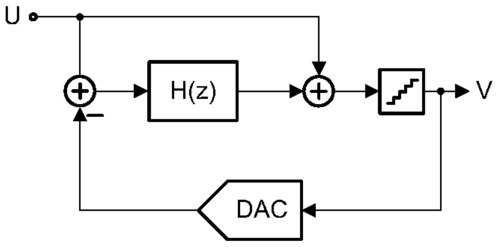
The block diagram of a DSM topology with input feedforwarding technique [5] is shown in Figure 1. It has been widely used to minimize the sensitivity to nonlinearities of components such as op-amps. Using this technique, the input forwarded into the quantizer directly can obtain a unity signal transfer function (STF) unaffected by the noise transfer function (NTF), and let the integrators process only the quantization noise. Hence, the performance requirements of integrators are relaxed, and the static power consumption of op-amps can be reduced by allowing a low voltage-swing operation. However, the conventional input feedforwarding technique proposed in [5] results in several drawbacks. First, a summing amplifier is required to combine the feedforward input and the integrator output before they are fed into the quantizer. Some publications [7,8] pursued modified input feedforwarding paths to the input of the last integrator, which eliminated the summing configuration but required differentiators instead. Second, it imposes a timing constraint from the feedforward input to the feedback DAC output worsened by data-weighted averaging (DWA). A publication [6] proposed a technique for relaxing the timing constraint but additional time-interleaved sampling circuits were required, causing a mismatch issue. Third, the implicit anti-aliasing filtering (AAF) characteristic of the CT ΔΣ ADC is drastically degraded, resulting in the use of an explicit AAF circuit. Fourth, the kickback noise injected from the quantizer to the input of the ADC results in a degraded overall performance. Therefore, a novel feedforwarding technique is required to overcome the drawbacks described above.

Figure 1.
Delta-sigma modulator (DSM) with input feedforwarding.
The VCO-based ADC adopts a quantizer utilizing a VCO, which can achieve the quantization of analog voltage with highly digital implementation consisting of a multi-phase ring oscillator and a counter. The basic operation of the VCO-based quantizer is to count the number of oscillation edges proportional to the input analog voltage [9]. Major advantages of the VCO-based ADC are simple implementation in a nanometer CMOS technology and easy integration of multi-bit quantization levels without using a large number of analog comparators whose operation is very sensitive to offset voltage and supply voltage scaling. It can also reduce the input capacitance when it is used in a multi-bit ΔΣ ADC configuration, and consume less power due to reduced load capacitance of the last loop filter stage. Another advantage of the VCO-based quantizer is the intrinsic first-order noise shaping for the quantization noise [9]. In addition, a DWA characteristic can be obtained inherently due to the identical barrel shifting pattern of the ring-oscillator outputs [10], which enables low power consumption and reduced excess loop delay (ELD) by having no explicit DWA circuit in CT ΔΣ ADC. However, VCO-based ADCs suffer from a nonlinear voltage-to-frequency characteristic of the VCO. To overcome this limitation, the residue-cancelling VCO-based quantizer [11] was proposed, as shown in Figure 2, where the nonlinearity of VCO was suppressed by processing only small residue of auxiliary ADC and DAC. However, this technique requires a precise conversion gain matching between paths VX-to-D1 and VX-to-D2. In addition, the use of additional flash ADC and DAC dictates an increase of power consumption and active area. Although a two-step VCO-based ADC [14] has been proposed to reject the nonlinearity of the VCO, it needs multiple VCO-based ADCs for one-order noise shaping and still requires precise gain matching between paths.
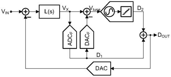
Figure 2.
Residue-cancelling VCO-based ΔΣ ADC [11].
3. Proposed VCO-Based ADC with Digital Feedback Residue Quantization
To overcome the drawback of requiring a summing amplifier in front of the quantizer in conventional input feedforwarding techniques, a novel digital input feedforwarding shown in Figure 3a is proposed. Here, a digitally converted input signal and a digital summing block substitutes the analog summing block in Figure 1. That is, the analog input signal (U) is quantized by an additional quantizer (Q2), whose output is added to the output of the original quantizer (Q1) in the digital domain. This digital summing block is easier to implement and consumes less power than the analog counterpart. However, the proposed digital input feedforwarding cannot overcome such drawbacks of the conventional input feedforwarding as worsening the timing constraint, degrading the AAF characteristic, and switching noise injection into the input. The non-unity gain of the added quantizer (Q2) may also cause an increased internal swing. To overcome these problems, note that the output signal (V) of an ordinary DSM in the frequency spectrum is composed of a digital version of the analog input and the quantization noise shaped to high-frequency region. Hence, relevant circuits in Figure 3a are modified such that the output in the digital domain, whose high-frequency quantization noise is suppressed by a digital low-pass filter (LPF), can be added to the quantizer output as depicted in the dotted box of Figure 3b, which is referred to as digital feedback residue quantization (DFRQ) technique.
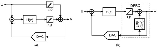
Figure 3.
Proposed swing reduction techniques: (a) digital input feedforwarding and (b) digital feedback residue quantization.
In Equation (2), the first and second terms on the right-hand side represent the STF and NTF, respectively. In this equation, note that, if , then , which implies that the proposed DSM with DFRQ can provide the same STF as that of the conventional input feedforwarding in the passband range of the digital LPF. Therefore, by employing the digital feedback of the low pass-filtered DSM output as in the proposed DSM, the quantizer can be made to process only the residual quantization noise.
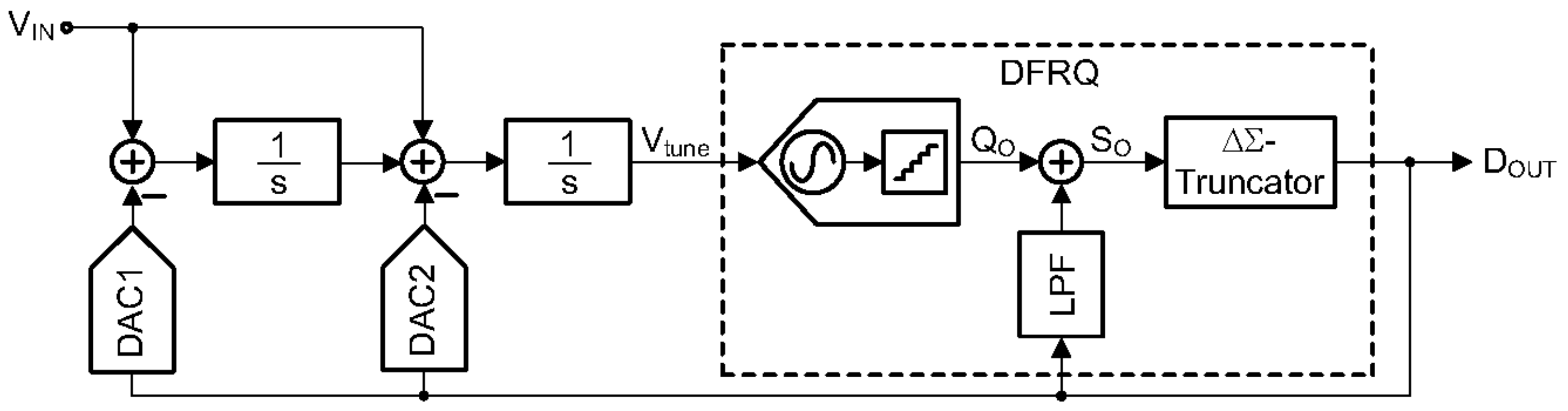
As described in Section 1, the continuous-time ΔΣ ADC using VCO-based quantizer is a good candidate as a high-speed low-power ADC but the VCO nonlinearity is a limiting factor. At this point, it is worth noting that the reduced voltage swing of the quantizer input of the proposed DFRQ lends itself to be well suited with VCO-based quantizer. Figure 4 shows the block diagram of the resulting VCO-based CT ΔΣ ADC adopting the proposed DFRQ. The DSM is composed of a CT loop filter with a second-order RC integrator, a five-bit feedback DAC, a VCO-based quantizer, a digital finite-impulse response (FIR) filter, a digital adder, and a ΔΣ truncator. By the proposed configuration, the third-order noise shaping is implemented by the second-order loop filter and the first-order intrinsic noise-shaping of the VCO-based quantizer. The structure of the VCO-based quantizer is shown in Figure 5, which consists of a starved inverter-based ring oscillator and counters. It can provide a quantized digital version of the analog input voltage by counting the number of oscillation edges in each clock cycle. The digital low-pass filtering to suppress high frequency quantization noise is implemented by a digital adder after the VCO-based quantizer and the digital FIR filter at the output of the DSM. The structure of the FIR filter is shown in Figure 6a, which is implemented using four taps. The timing constraint of the proposed DFRQ to ensure loop stability of the digital feedback composed of the ΔΣ-truncator and LPF requires that the DFRQ should operate in one clock cycle. To ensure the overall loop stability of CT DSMs, an excess loop delay (ELD) compensation scheme can be used [16,17,18].

Figure 4.
VCO-based CT ΔΣ ADC with DFRQ.
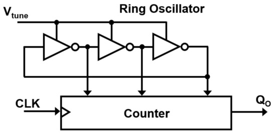
Figure 5.
VCO-based quantizer.
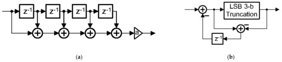
Figure 6.
(a) Four-tap digital FIR filter, (b) first-order ΔΣ truncator.
To sufficiently suppress the residual quantization noise in the DFRQ, the FIR filter with a larger number of taps should be used, resulting in an increased number of output bits. This also increases the levels of the feedback DAC, increasing the complexity of the DAC and tightening the timing requirement imposed on the DWA and DAC operation. As a result, the quantizer and the feedback DAC may consume a large dynamic power. Therefore, in our design, the first-order error feedback ΔΣ truncator [19] shown in Figure 6b is used. One cycle-delayed version of the truncated least significant bits (LSBs) is fed and added to the input to allow the truncation error to be first-order shaped. Thus, the ΔΣ truncator reduces the output bits increased by the four-tap FIR filter and the adder in the DFRQ, and avoids the SNDR degradation by the error due to truncation. Note that the accuracy of the filter coefficient does not affect the overall performance because the LPF determines only the suppression ratio of the shaped out-of-band noise.
The unique structure of the proposed DSM with DFRQ results in overall power reduction in the loop filter as well as in the quantizer since the static power consumption of op-amps in the loop filter and the dynamic power consumption of the multi-bit quantizer can be reduced due to lower voltage swing. For example, a reduced voltage swing at the integrator output can help avoid the op-amp stage for increasing the signal swing, It can also reduce the amount of charge deposited into the integrating capacitor, which can avoid the use of a slew-rate enhancement scheme [20]. The proposed DFRQ technique can further reduce the power consumption and silicon area by removing the summing amplifier in front of the quantizer, and relieving the timing constraint from the input to the feedback DAC. Since it does not have a direct signal path from the input to the quantizer, no switching noise is injected into the input, which helps increase the immunity to electromagnetic interference (EMI) [21]. Moreover, unlike the conventional input feedforwarding, there is no degradation on intrinsic AAF characteristic of CT ΔΣ ADC. It can also reduce the input swing of the quantizer and allows a reduced number of comparators to be used in a traditional flash quantizer [22,23,24,25]. The reduced voltage swing at the input of the quantizer in the proposed DSM helps relieve the nonlinearity problem of the VCO-based quantizer. It can also allow a third-order noise shaping using a second-order loop filter due to intrinsic noise shaping feature of the VCO. Finally, it is noted that, although an intrinsic DWA property can be supported by the barrel shifting of the VCO quantizer in the proposed design, the property can be lost by the conversion into a digital code. Therefore, when going back to the analog domain, an explicit DWA may be needed.
4. Simulation Results
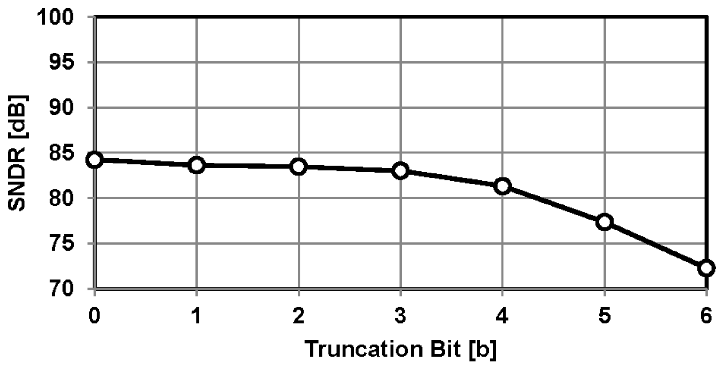
To assess the performance, the VCO-based CT ΔΣ ADC with DFRQ was designed, and the effectiveness was verified by simulation using Matlab. Our design was targeting a 2-MHz signal bandwidth with both SNDR and DR above 80 dB in a 28-nm CMOS technology node. The nonlinearity of the VCO in the quantizer was modeled by hyperbolic tangent function [13]. The signal bandwidth for the simulation was 2-MHz with a sampling frequency of 80-MHz (OSR = 20). As mentioned in the description of the proposed architecture, the number of truncation bits in the ΔΣ truncator is a trade-off between the performance of SNDR and the number of output bits determining the levels of the feedback DAC and the complexity of the post digital decimation filter. In Figure 7, the simulated SNDR of the proposed architecture depending on the number of truncation bits in the first-order ΔΣ truncator is depicted. Three-bit truncation (eight-to-five truncation) is selected in our design for providing a minimum SNDR degradation with moderate increase of feedback DAC levels.

Figure 7.
SNDR versus truncation bits.
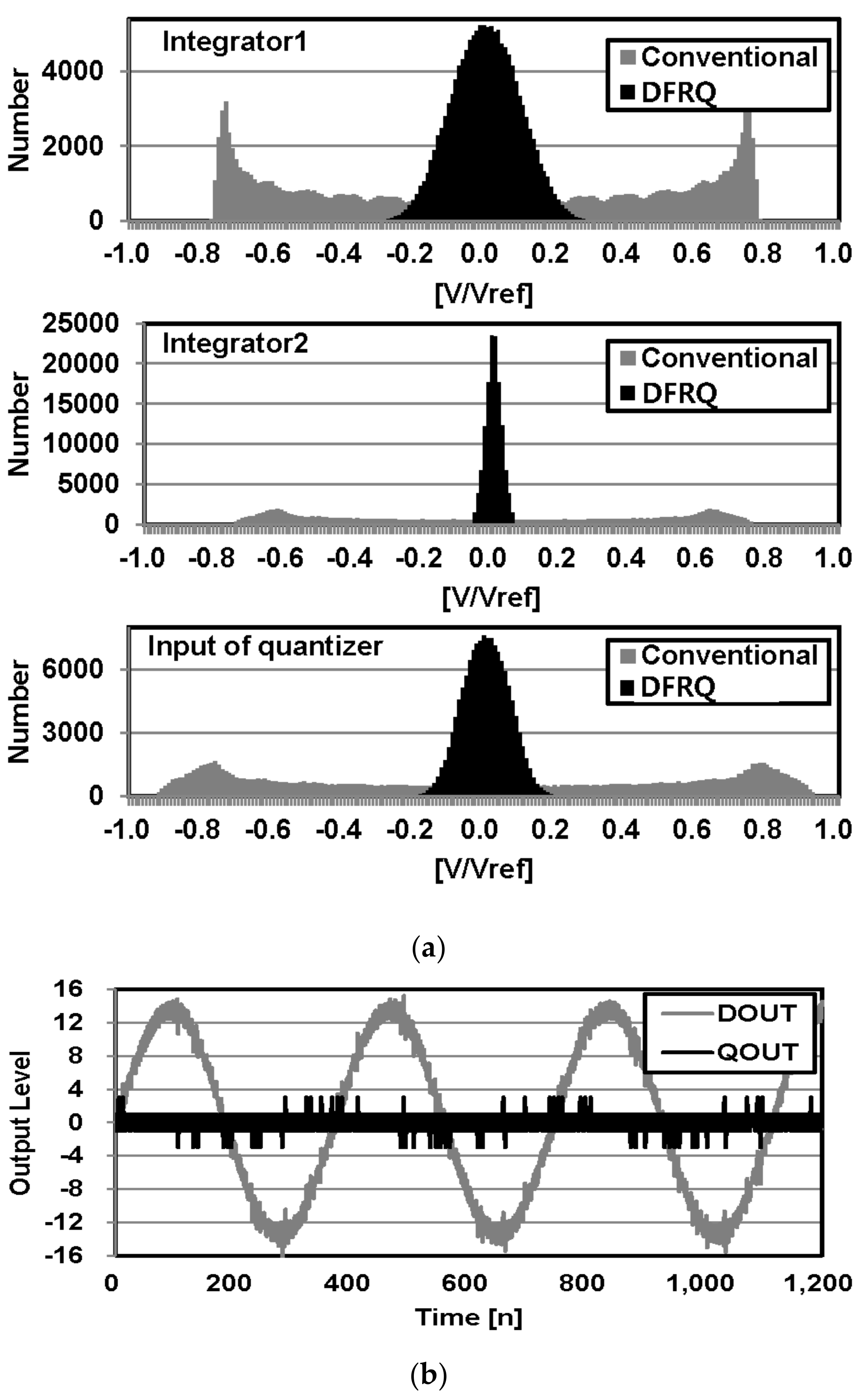
Figure 8 shows the simulated histograms for the output voltage swing of major circuit components and the transient waveforms of the second-order four-bit DT DSM with DFRQ and the traditional cascade integrator feedback (CIFB) DSM without input feedforwarding. As seen in Figure 8a, the integrator output swing of the proposed DSM is reduced by 75~90% as compared to the conventional DSM. Figure 8b also shows the output waveforms of the DSM and the quantizer in the DFRQ, indicating the swing reduction of the quantizer in the proposed technique. Note that, as mentioned in the previous section, the advantage of reduced voltage swing is obtained without causing the problems of conventional input feedforwarding techniques, such as increased timing constraint, degraded AAF characteristic, and switching noise injection into the input.
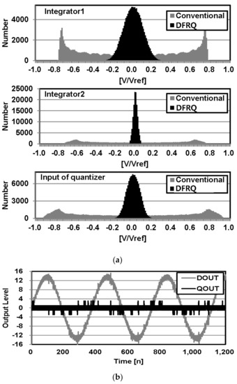
Figure 8.
Simulated voltage swing histograms and transient waveforms of the proposed DFRQ and the traditional DSM: (a) histograms of internal node voltage swing at the first and second integrator outputs and the quantizer input, (b) waveforms at DSM and quantizer outputs (DOUT and QOUT) for the DFRQ.
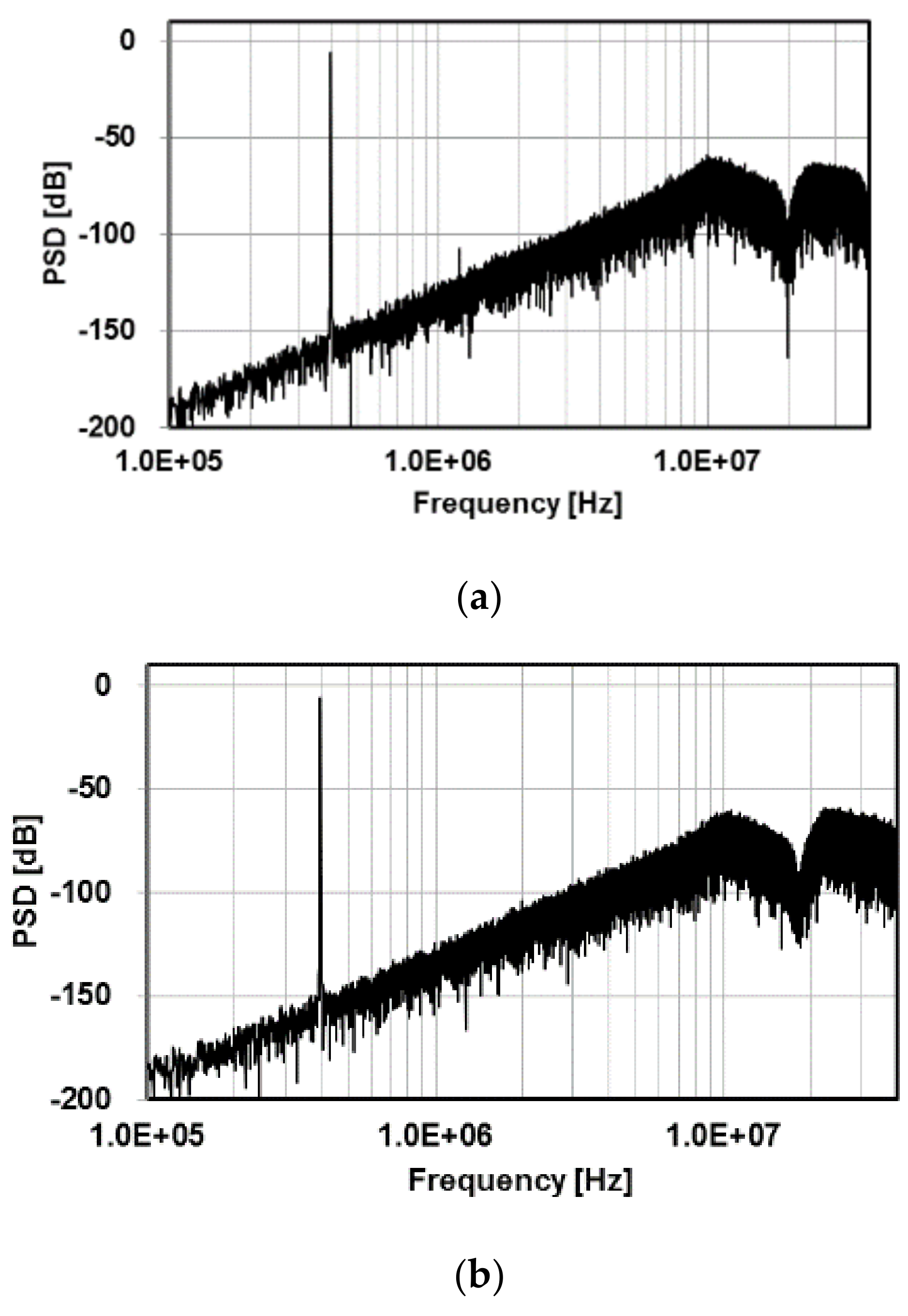
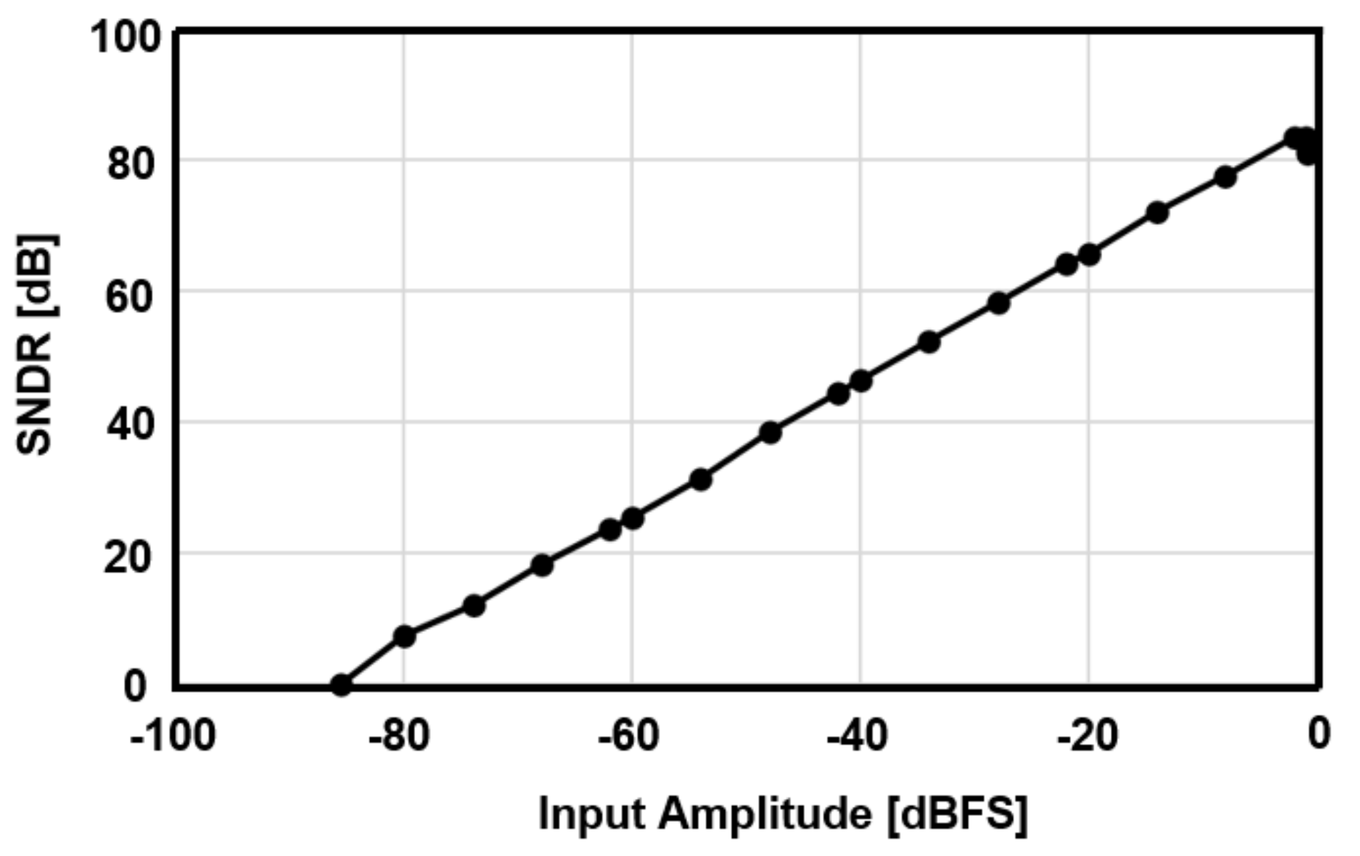
Figure 9 shows the simulated power spectral density (PSD) of the VCO-based CT ΔΣ ADC with and without DFRQ. The quantization nose is high-pass filtered by 60-dB per decade with third-order noise shaping by the second-order CT loop filter and the intrinsic first-order noise shaping of the VCO-based quantizer. As seen in Figure 9a, for the conventional VCO-based ADC, the nonlinearity of the VCO causes a −58-dB second harmonic and a −63-dB third harmonic, which deteriorates the overall SNDR from 84.2-dB to 53.2-dB. Meanwhile, for the proposed VCO-based ADC, the proposed DFRQ allows the input voltage swing of the VCO-based quantizer to be reduced, resulting in the overall operation being less affected by the nonlinearity of the VCO. Therefore, as seen in Figure 9b, the proposed VCO-based CT ΔΣ ADC suppress all the harmonics in Figure 9a and restores the SNDR from 53.2-dB to 83.5-dB. The NTF gain at high frequencies is slightly increased due to nonideal low-pass filtering of the shaped quantization noise in the 4-tap FIR filter. Figure 9c shows the PSD of the proposed ADC obtained at 2-MHz input frequency which is the highest in-band frequency for the verification of the DFRQ stability. It shows a stable operation of the proposed DSM without performance degradation despite the timing requirement becomes tighter at higher input frequency. Figure 10a,b show the PSDs of the LPF outputs in the DFRQ without and with the filter coefficient variation, respectively. Basically, the PSD of the filter will not be affected by its coefficient variation since the filter is implemented in the digital domain. However, as shown in Figure 10b, the inaccuracy of the filter coefficients can slightly degrade the notch filter characteristic in the out-of-band region, which does not affect the overall performance as mentioned in the previous section. Simulated SNDR as a function of input amplitude is plotted in Figure 11.
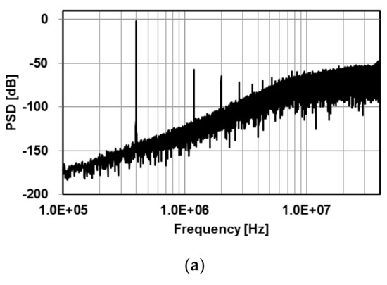
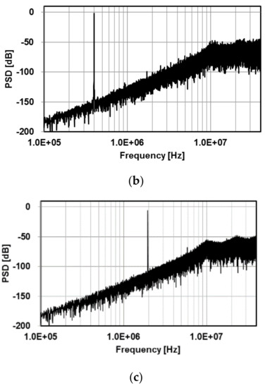
Figure 9.
Simulated power spectral density (PSD) of VCO-based CT ΔΣ ADC: (a) without and (b) with DFRQ, and (c) with DFRQ under high frequency input around in-band edge.

Figure 10.
PSD of digital LPF output as the accuracy of filter coefficient: (a) ideal; (b) with 20% variation.

Figure 11.
SNDR versus input amplitude.
As stated earlier, the proposed VCO-based CT ΔΣ ADC with DFRQ can reduce the power consumption and silicon area of the analog domain in the system. On the other hand, the design complexity and power consumption in the digital domain may increase due to increased digital components. However, the design in digital domain can migrate to an advanced deep-submicron digital process available, taking advantage of low-voltage design and compactness of highly digital implementation. Therefore, the proposed architecture can improve power efficiency by moving ΔΣ ADC design efforts from the analog to digital domain. Table 1 shows the performance comparison for several ΔΣ ADCs including conventional designs with either input forwarding [7,8] or VCO-based quantizer [9,10,12,13].

Table 1.
Performance comparison of continuous-time delta-sigma ADCs.
5. Conclusions
In this paper, a novel feedforwarding technique based on a digital feedback residue quantization (DFRQ) is proposed to avoid analog summing amplifier, maintain intrinsic anti-aliasing filtering (AAF) characteristic, and inject no switching noise into input. A VCO-based ΔΣ ADC with the proposed DFRQ is also presented to avoid the degradation of signal-to-noise and distortion (SNDR) by suppressing the nonlinearity of the VCO quantizer. Evaluation results indicated that the VCO-based CT ΔΣ ADC with DFRQ achieved a substantial SNDR improvement.
Author Contributions
M.-Y.C. designed the circuits, performed the simulation and implementation, analyzed the measurement data, and wrote the manuscript. B.-S.K. funding acquired, supervised, reviewed, wrote, and edited the manuscript. All authors have read and agreed to the published version of the manuscript.
Funding
This research received no external funding.
Acknowledgments
This work was partly supported by the NRF grant funded by MSIT (2019R1A2C1011155).
Conflicts of Interest
The authors declare no conflict of interest.
References
- Jindal, S.; Manhas, S.K.; Gautam, S.K.; Balatti, S.; Kumar, A.; Pakala, M. Investigation of Gate-Length Scaling of Ferroelectric FET. IEEE Trans. Electron. Devices 2021, 68, 1364–1368. [Google Scholar] [CrossRef]
- Tan, Z.; Chen, C.-H.; Chae, Y.; Temes, G.C. Incremental Delta-Sigma ADCs: A Tutorial Review. IEEE Trans. Circuits Syst. I Regul. Pap. 2020, 67, 4161–4173. [Google Scholar] [CrossRef]
- Shakya, J.R.; Temes, G.C. Efficient Calibration of Feedback DAC in Delta Sigma Modulators. IEEE Trans. Circuits Syst. II Express Briefs 2020, 67, 826–830. [Google Scholar] [CrossRef]
- Geerts, Y.; Steyaert, M.; Sansen, W. A High-Performance Multibit/Spl Delta//Spl Sigma/CMOS ADC. IEEE J. Solid-State Circuits 2000, 35, 1829–1840. [Google Scholar] [CrossRef]
- Silva, J.; Moon, U.; Steensgaard, J.; Temes, G. Wideband Low-Distortion Delta-Sigma ADC Topology. Electron. Lett. 2001, 37, 737–738. [Google Scholar] [CrossRef]
- Gharbiya, A.; Johns, D.A. On the Implementation of Input Feedforward Delta-Sigma Modulators. IEEE Trans. Circuits Syst. II Express Briefs 2006, 53, 383–387. [Google Scholar] [CrossRef] [Green Version]
- Lee, K.; Temes, G. Improved Architecture for Low-Distortion ADCs. Electron. Lett. 2009, 45, 730–731. [Google Scholar] [CrossRef]
- Jung, Y.; Roh, H.; Roh, J. An Input-Feedforward Multibit Adder-Less Δ − Σ Modulator for Ultrasound Imaging Systems. IEEE Trans. Instrum. Meas. 2013, 62, 2215–2227. [Google Scholar] [CrossRef]
- Straayer, M.Z.; Perrott, M.H. A 12-Bit, 10-MHz Bandwidth, Continuous-Time ΣΔ ADC with a 5-Bit, 950-MS/s VCO-Based Quantizer. IEEE J. Solid-State Circuits 2008, 43, 805–814. [Google Scholar] [CrossRef]
- Park, M.; Perrott, M.H. A 78 dB SNDR 87 mW 20 MHz Bandwidth Continuous-Time ΔΣ ADC with VCO-Based Integrator and Quantizer Implemented in 0.13 µm CMOS. IEEE J. Solid-State Circuits 2009, 44, 3344–3358. [Google Scholar] [CrossRef]
- Reddy, K.; Rao, S.; Inti, R.; Young, B.; Elshazly, A.; Talegaonkar, M.; Hanumolu, P.K. A 16-mW 78-dB SNDR 10-MHz BW CT Δ Σ ADC Using Residue-Cancelling VCO-Based Quantizer. IEEE J. Solid-State Circuits 2012, 47, 2916–2927. [Google Scholar] [CrossRef]
- Zaliasl, S.; Saxena, S.; Hanumolu, P.K.; Mayaram, K.; Fiez, T.S. A 12.5-Bit 4 MHz 13.8 mW MASH Δ Σ Modulator with Multirated VCO-Based ADC. IEEE Trans. Circuits Syst. I Regul. Pap. 2012, 59, 1604–1613. [Google Scholar] [CrossRef]
- Colodro, F.; Torralba, A. Linearity Enhancement of VCO-Based Quantizers for SD Modulators by Means of a Tracking Loop. IEEE Trans. Circuits Syst. II Express Briefs 2014, 61, 383–387. [Google Scholar] [CrossRef]
- Xing, X.; Gielen, G. A 42 fJ/Step-FoM Two-Step VCO-Based Delta-Sigma ADC in 40 nm CMOS. IEEE J. Solid-State Circuits 2015, 50, 714–723. [Google Scholar] [CrossRef]
- Zhu, P.; Xing, X.; Gielen, G. A 40-MHz Bandwidth 0–2 MASH VCO-Based Delta-Sigma ADC With 35-fJ/Step FoM. IEEE Trans. Circuits Syst. II Express Briefs 2015, 62, 952–956. [Google Scholar] [CrossRef]
- Kim, T.; Han, C.; Maghari, N. A 7.2 mW 75.3 dB SNDR 10 MHz BW CT Delta-Sigma Modulator Using Gm-C-Based Noise-Shaped Quantizer and Digital Integrator. IEEE J. Solid-State Circuits 2016, 51, 1840–1850. [Google Scholar] [CrossRef]
- Pavan, S. Excess Loop Delay Compensation in Continuous-Time Delta-Sigma Modulators. IEEE Trans. Circuits Syst. II Express Briefs 2008, 55, 1119–1123. [Google Scholar] [CrossRef]
- Keller, M.; Buhmann, A.; Sauerbrey, J.; Ortmanns, M.; Manoli, Y. A Comparative Study on Excess-Loop-Delay Compensation Techniques for Continuous-Time Sigma–Delta Modulators. IEEE Trans. Circuits Syst. I Regul. Pap. 2008, 55, 3480–3487. [Google Scholar] [CrossRef]
- Singh, V.; Krishnapura, N.; Pavan, S.; Vigraham, B.; Behera, D.; Nigania, N. A 16 MHz BW 75 dB DR CT ΔΣ ADC Compensated for More Than One Cycle Excess Loop Delay. IEEE J. Solid-State Circuits 2012, 47, 1884–1895. [Google Scholar] [CrossRef]
- Pavan, S.; Sankar, P. Power Reduction in Continuous-Time Delta-Sigma Modulators Using the Assisted Opamp Technique. IEEE J. Solid-State Circuits 2010, 45, 1365–1379. [Google Scholar] [CrossRef]
- Tsai, H.-C.; Lo, C.-L.; Ho, C.-Y.; Lin, Y.-H. A 64-fJ/Conv.-Step Continuous-Time Σ Δ Modulator in 40-nm CMOS Using Asynchronous SAR Quantizer and Digital ΔΣ Truncator. IEEE J. Solid-State Circuits 2013, 48, 2637–2648. [Google Scholar] [CrossRef]
- Nguyen, K.; Adams, R.; Sweetland, K.; Chen, H. A 106-dB SNR hybrid oversampling analog-to-digital converter for digital audio. IEEE J. Solid-State Circuits 2005, 40, 2408–2415. [Google Scholar] [CrossRef]
- Dorrer, L.; Kuttner, F.; Greco, P.; Torta, P.; Hartig, T. A 3-mW 74-dB SNR 2-MHz Continuous-Time Delta-Sigma ADC with a Tracking ADC Quantizer in 0.13-/spl mu/m CMOS. IEEE J. Solid-State Circuits 2005, 40, 2416–2427. [Google Scholar] [CrossRef]
- Pesenti, S.; Clement, P.; Kayal, M. Reducing the Number of Comparators in Multibt Δ Σ Modulators. IEEE Trans. Circuits Syst. I Regul. Pap. 2008, 55, 1011–1022. [Google Scholar] [CrossRef]
- Colodro, F.; Torralba, A. Continuous-Time Sigma–Delta Modulator with a Fast Tracking Quantizer and Reduced Number of Comparators. IEEE Trans. Circuits Syst. I Regul. Pap. 2010, 57, 2413–2425. [Google Scholar] [CrossRef]


Publisher’s Note: MDPI stays neutral with regard to jurisdictional claims in published maps and institutional affiliations. |
© 2021 by the authors. Licensee MDPI, Basel, Switzerland. This article is an open access article distributed under the terms and conditions of the Creative Commons Attribution (CC BY) license (https://creativecommons.org/licenses/by/4.0/).