Abstract
A novel power amplifier unit for a phased array radar with 2 × 2 output ports for a vacuum electron device is proposed. Double parallel connecting microstrip meander-lines are employed as the slow-wave circuits of a large power traveling wave tube operate in a Ka-band. The high frequency characteristics, the transmission characteristics, and the beam–wave interaction processes for this amplifier are simulated and optimized. For each output port of one channel, the simulation results reveal that the output power, saturated gain, and 3-dB bandwidth can reach 566 W, 27.5 dB, and 7 GHz, respectively. Additionally, the amplified signals of four output ports have favorable phase congruency. After fabrication and assembly, transmission tests for the 80-period model are performed preliminarily. The tested “cold” S-parameters match well with the simulated values. This type of integratable amplifier combined with a vacuum device has broad application prospects in the field of high power and broad bandwidth on a millimeter wave phased array radar.
1. Introduction
Phased array radar (PAR) has displayed great advantages to users in recent years [1,2]. As the most critical components, transmit/receive (T/R) modules occupy about 70% percent of the PAR antennas. As the terminal amplification component in the transmit link of the T/R modules, the power amplifier (PA) always determines the transmit distance of the PAR. A lightweight, low-voltage, compact and broadband PA with large power at millimeter-wave frequencies (30~100 GHz) is probably satisfied by the requirements of the T/R modules in PAR [3,4].
Traditionally, solid-state semiconductors, such as GaAs and even GaN PA, are widely used in the design of T/R modules [5,6]. For instance, the GaN PA in Ka-band is capable of tens of watts of output power with a bandwidth up to 2 GHz, which could indicate potential improvements both on power and bandwidth. In recent years, vacuum electronic devices have developed rapidly and show great potential at the millimeter wave frequency range and even on the THz spectrum. Both with high power output and broad bandwidth, the traveling-wave tube (TWT) has been widely used in electronic counters, transmitters, and communications [7].
Due to a relatively larger volume and incompatibility to solid-state circuits, TWTs are always placed separately for each transmit channel in a large power active PAR. This traditional framework is not only expensive, but also heavy and bulky, so it has many limitations for application. As we have developed micro-fabrication technologies, the production requirements for novel slow-wave structures (SWSs) are probably met in the millimeter-wave frequency range [8,9]. Among these SWSs, the microstrip meander-line (MML) has been proven to be suitable for low-voltage and broadband TWTs [10,11]. It is also naturally easy to integrate with solid-state circuits and has superiority over the volume.
Motivated by the applications of PARs, a novel broadband 2 × 2 amplifier unit with a large power TWT is proposed in this paper. This novel framework has potential for applying the TWT to the terminal PA in the transmit link of the T/R modules. The simulation results show that these amplifier units are capable of delivering kW-class output power fully with a 3-dB bandwidth of more than 7 GHz in the Ka-band. Moreover, the simulation results show that the phase congruency at the four out ports is great.
The remainder of this paper is organized as follows. Section 2 presents the system model, which includes the novel SWS design and the whole input coupling structure. Simulation results are presented in Section 3. In Section 4, we present our fabrication and experimental tests, and compare the results with the simulation. The final conclusions are presented in Section 5.
2. Structure Description
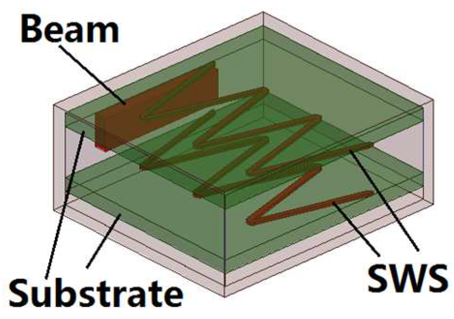
Easy to be integrated with a solid-state circuit, the MML SWS can be printed with micro fabrication technologies. Of all the modified and improved MML SWSs, the symmetrical double V-shaped MML with higher electron efficiency has been investigated in detail in reference [12]. The schematic of the symmetric double V-shaped MML is shown in Figure 1.

Figure 1.
Sketch of the symmetric double V-shape MML SWS.
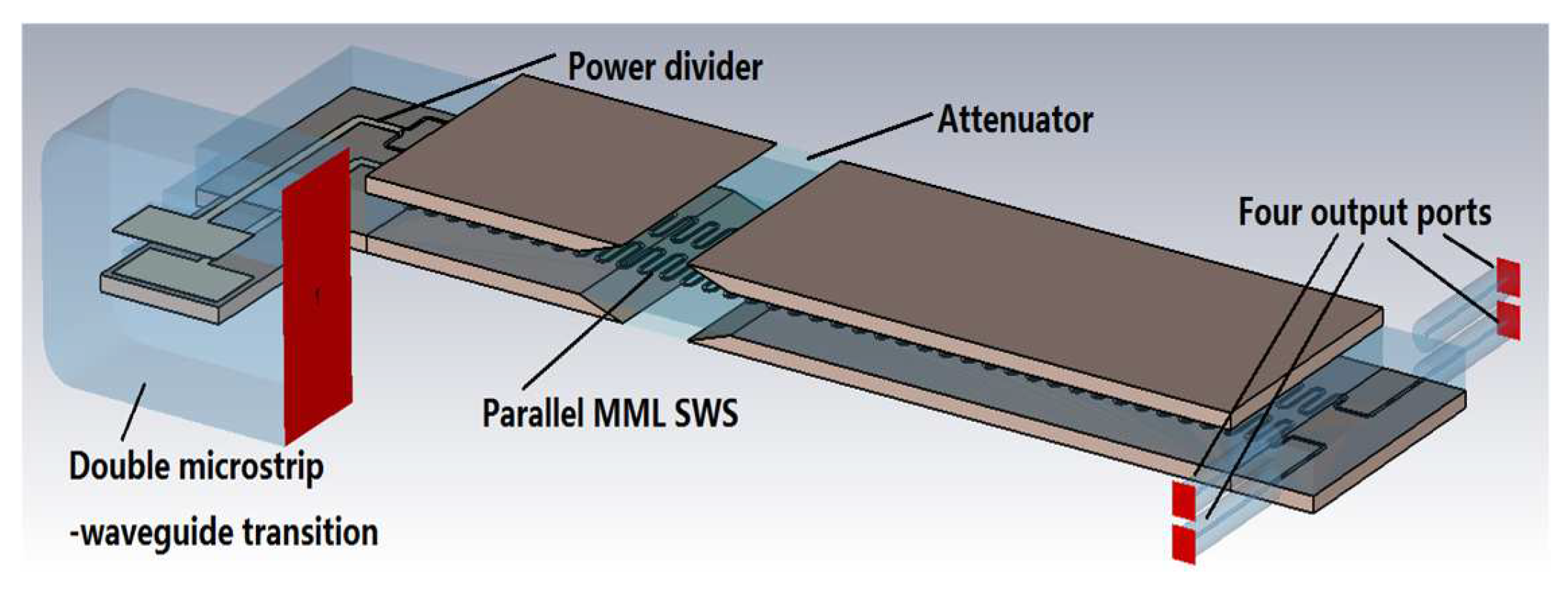
Inspired by the above TWTs, we propose a novel SWS by parallel, connecting two MMLs together, and then symmetrical, placing them on both the top and bottom dielectric substrates of the cavity to form the four output ports. The two parallel MMLs are connected to each other by power dividers at the end and the whole input coupling structure is designed as a double microstrips–rectangular waveguide transition. Four coaxial cable output ports are connected to the SWS with microstrip lines. Two tapered attenuators are symmetrically inserted into the SWS to suppress the oscillations. The sketch of the novel SWS is shown in Figure 2, in which this 2 × 2 unit consists of one rectangular waveguide input port and four coaxial output ports. One sheet electron beam gun is employed in the beam–wave interaction processes of the TWT to further reduce the whole volume and weight.

Figure 2.
System schematic of the novel 2 × 2 amplifier units.
The operation principle of the amplifier is based on typical O-type vacuum electronic devices. To achieve multi-output, the double microstrips–rectangular waveguide transition and the power divider are employed in the structure. The electron beam is emitted by the electron gun and focused by the focus magnetic field, and then enters into the interaction space. Meanwhile, the input signal is imported into the top and bottom MMLs through the double microstrips and rectangular waveguide transitions, respectively. Then, the signals on the top and bottom MMLs are both divided into two signals by the power divider and transmitted along the four parallel MML SWSs. The four independent signals stimulate radio-frequency fields around the MML SWSs and interact with electron beams. As most of the electrons are decelerated, some kinetic energy from the sheet electron beam is transferred to the radio-frequency fields and the four signals are amplified respectively. At last, the 2 × 2 amplified signals are exported by the four coaxial cable output ports.
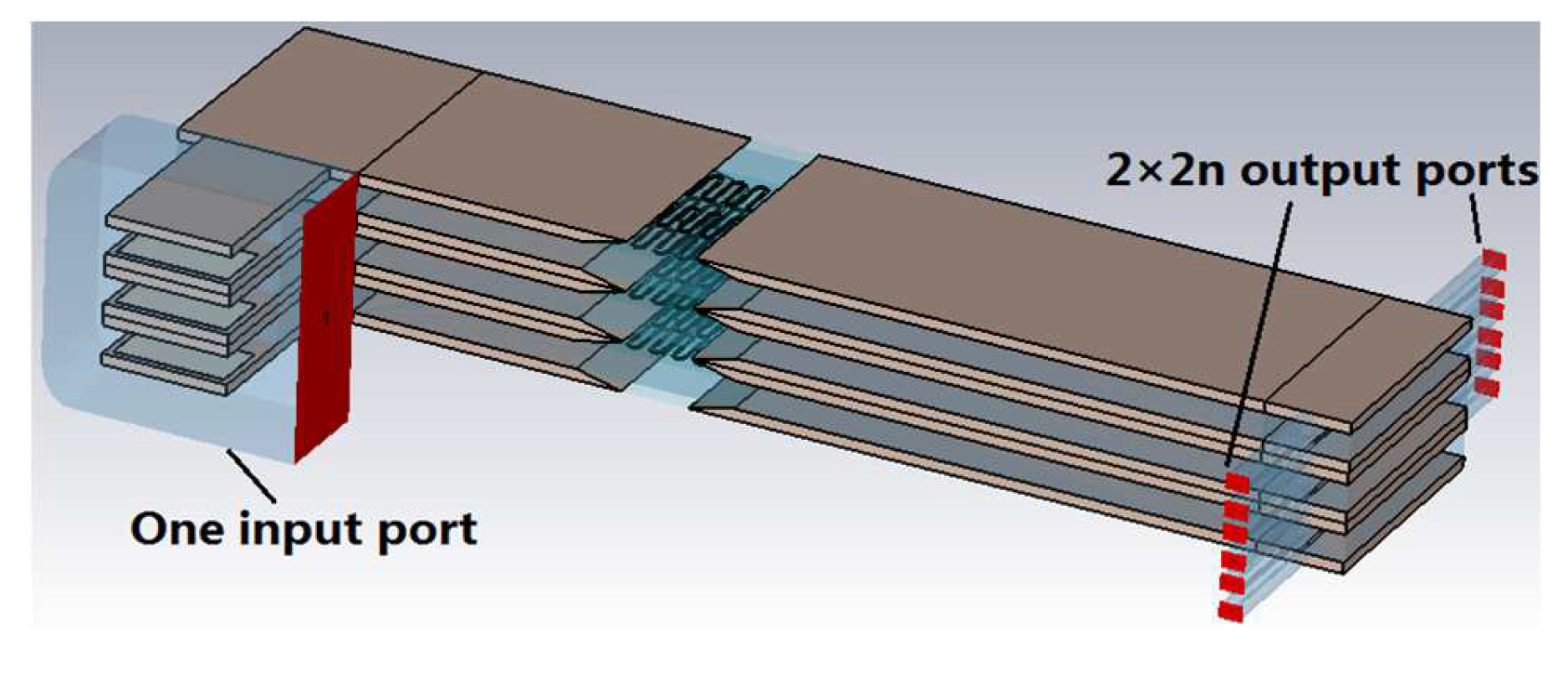
This 2 × 2 amplifier unit is probably integrated for larger scale units with multiple methods for application in the T/R modules of the PARs. Based on the development of the multi-beam electron gun [13], one possible framework to compose 2 × 2n units is to simply pile up the units vertically as in Figure 3, in which n is the quantity of the 2 × 2 amplifier unit. In this integrated framework, the input ports can be designed as overall input ports, or even directly connect to the preamp circuit by microstrip lines.
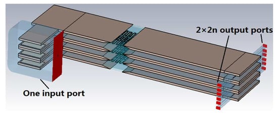
Figure 3.
A possible framework for integrated 2 × 2n units.
3. Simulation Results
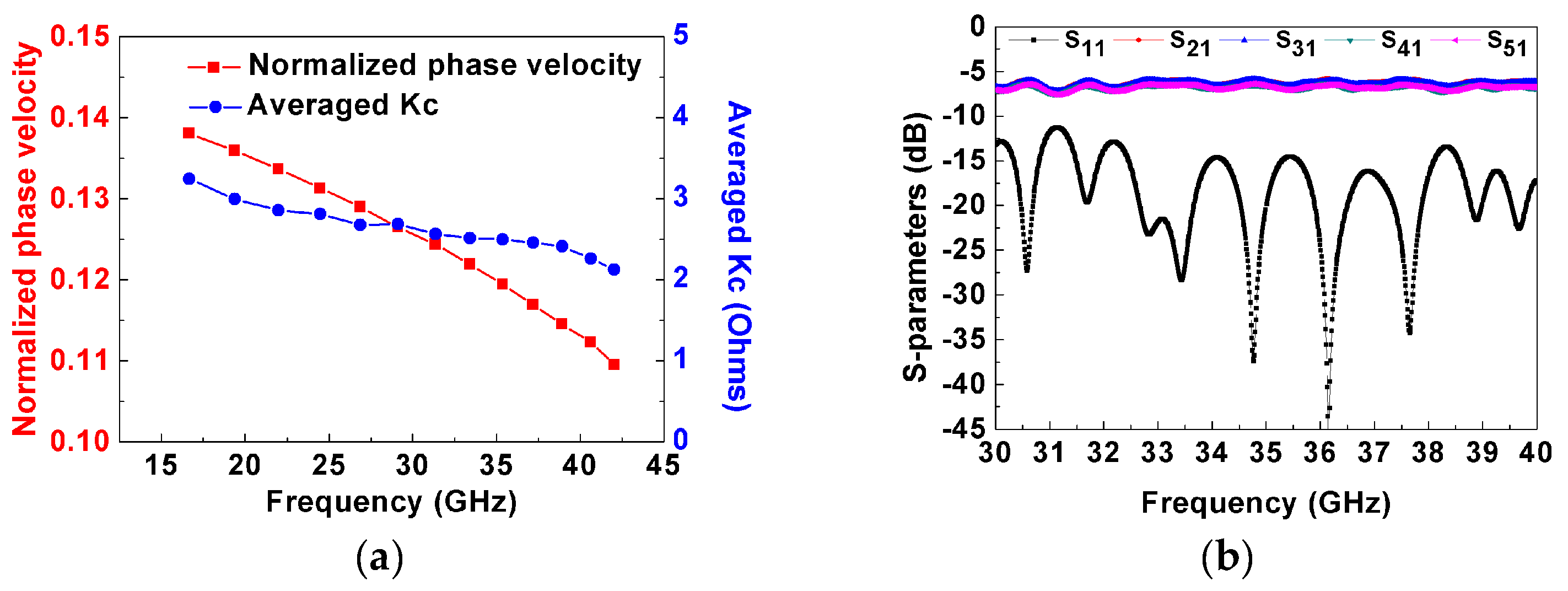
The high frequency characteristics, including dispersion curves and average interaction impedances for a single period, are first investigated. It can be seen in Figure 4a that the dispersion curves are flat in the frequency between 20 GHz and 40 GHz, which indicates that the cold bandwidth is relatively broad. The averaged interaction impedances (Kc) over the cross section of the electron beam can accurately predict the beam–wave interaction efficiency. According to the transverse parameters of the SWS, the cross section of the electron beam is set to be 2.12 mm × 0.3 mm. The average coupling impedances can reach 2.5 Ohms in the operation frequency band.
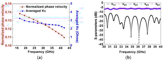
Figure 4.
Plot of the dispersion curve (red) and the averaged interaction impedances (blue) versus frequency (a); S-parameters of the transmission model (b).
The transmission model without an attenuator is optimized by CST Microwave Studio [14], including 80-period SWS, the input and output coupling structures, and the power combiners, to reduce reflection and improve transmission efficiency. The material of the dielectric substrates is set to Rogers RT5880, with a relative permittivity and dielectric dissipation factor of 2.2 and 0.0009, respectively. The dimensional parameters of the SWS in the simulations are listed in Table 1.

Table 1.
Dimensional parameters of the SWS.
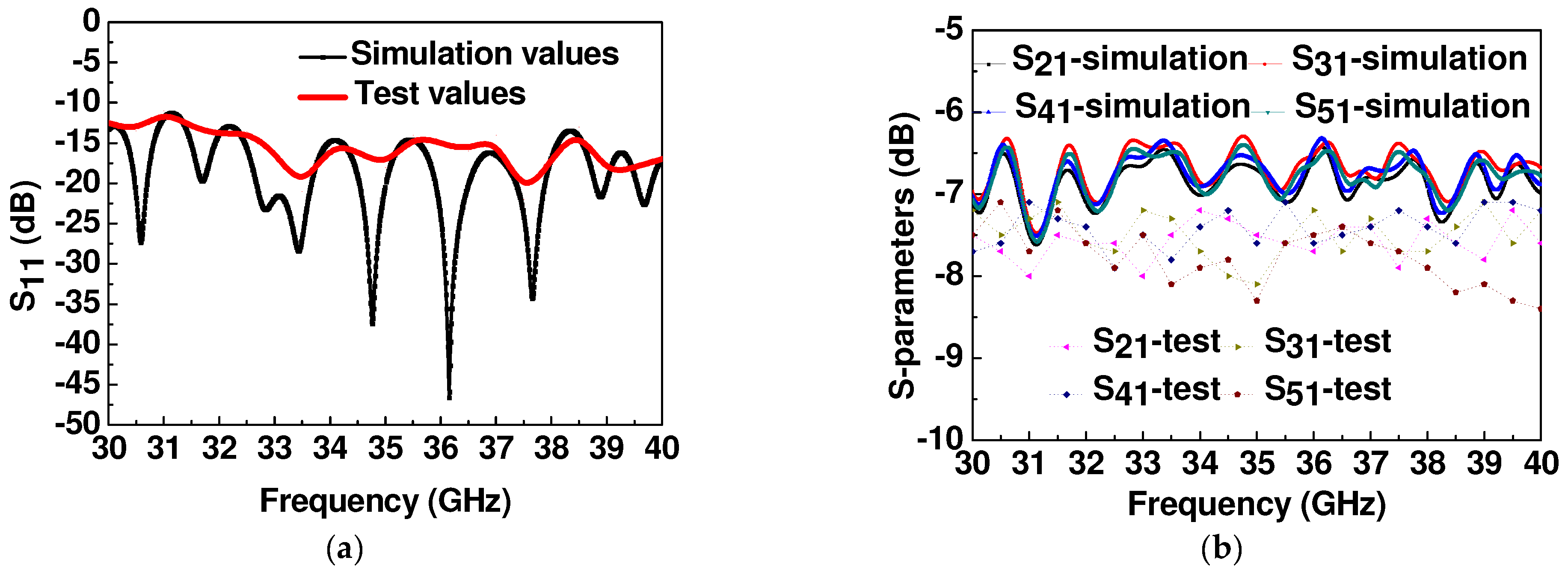
The S11 parameters are generally below −16 dB and between 33 GHz and 38 GHz, as shown in Figure 4b. The almost coincided S21, S31, S41 and S51 curves with amplitudes larger than −7 dB indicate symmetry and uniformity for the four output ports.
In order to verify the beam–wave interaction of the novel structure, the whole amplifier model of the novel TWT shown in Figure 2 is built by CST. Two beryllia attenuators are symmetrically inserted into the SWS to suppress the oscillations. The attenuators are optimally designed as a tapered shape to absorb reflected waves over a wide range of frequencies. Driven by only one sheet electron beam with large width–thickness ratio, the beam–wave interaction processes of the novel TWT amplifier are investigated.
More than 3.5 million particles and 8.3 million meshes are used in the particle-in-cell (PIC) simulation. The electrical parameters of the TWT shown in Table 2 have already been optimized by utilizing CST Particle Studio software. The beam voltage, current, and the focus magnetic field in the TWT simulation are set to 5100 V, 1 A, and 0.8 T, respectively. Here we specify the physical meaning of each variables in CST Particle Studio as follows [14]: the sheet beam voltage indicates the kinetic start energy of the emitted particles; the sheet beam current indicates the emission current; the input signal amplitude indicates the amplitude of the input sine step signal; the focus magnetic field indicates the amplitude of a constant focus magnetic field inside the whole computational domain; the center frequency indicates the designed center operation frequency of the amplifier.
Table 2.
Optimized electrical parameters for the TWT.
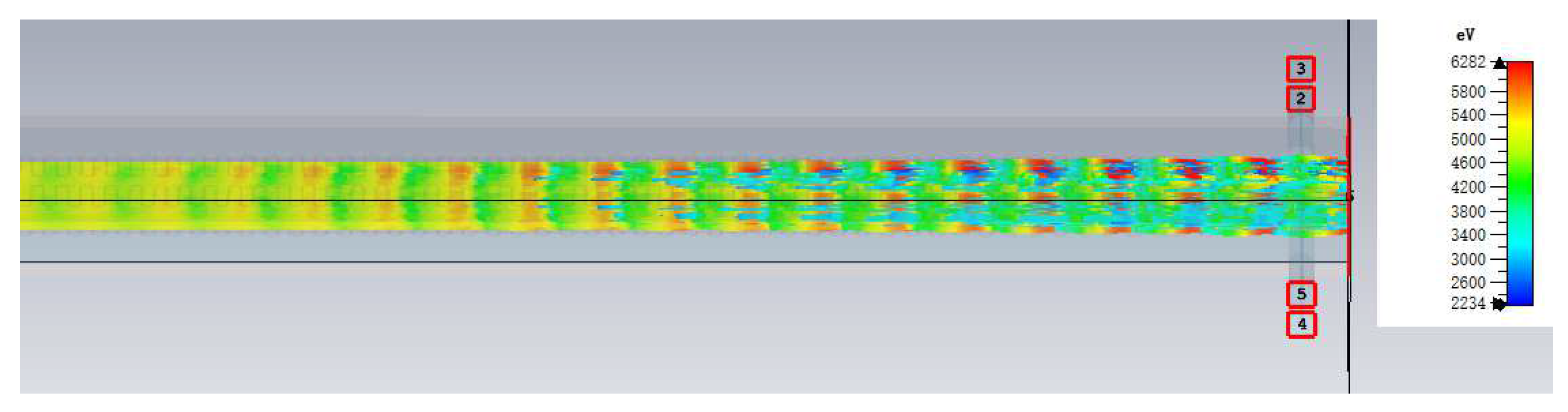
The PIC simulation results at a frequency of 35 GHz are shown Figure 5, Figure 6, Figure 7, Figure 8, Figure 9. Figure 5 depicts the electron bunching phenomenon in a TWT operation, where we can see that the accelerating electrons and retarding electrons are periodically arranged along a longitudinal direction, which demonstrates a good beam–wave energy exchange process. This physical phenomenon is very typical in O-type vacuum electronic devices.

Figure 5.
Typical electron bunching along a longitudinal direction.
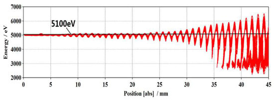
Figure 6.
Electron kinetic energy versus longitudinal distance.

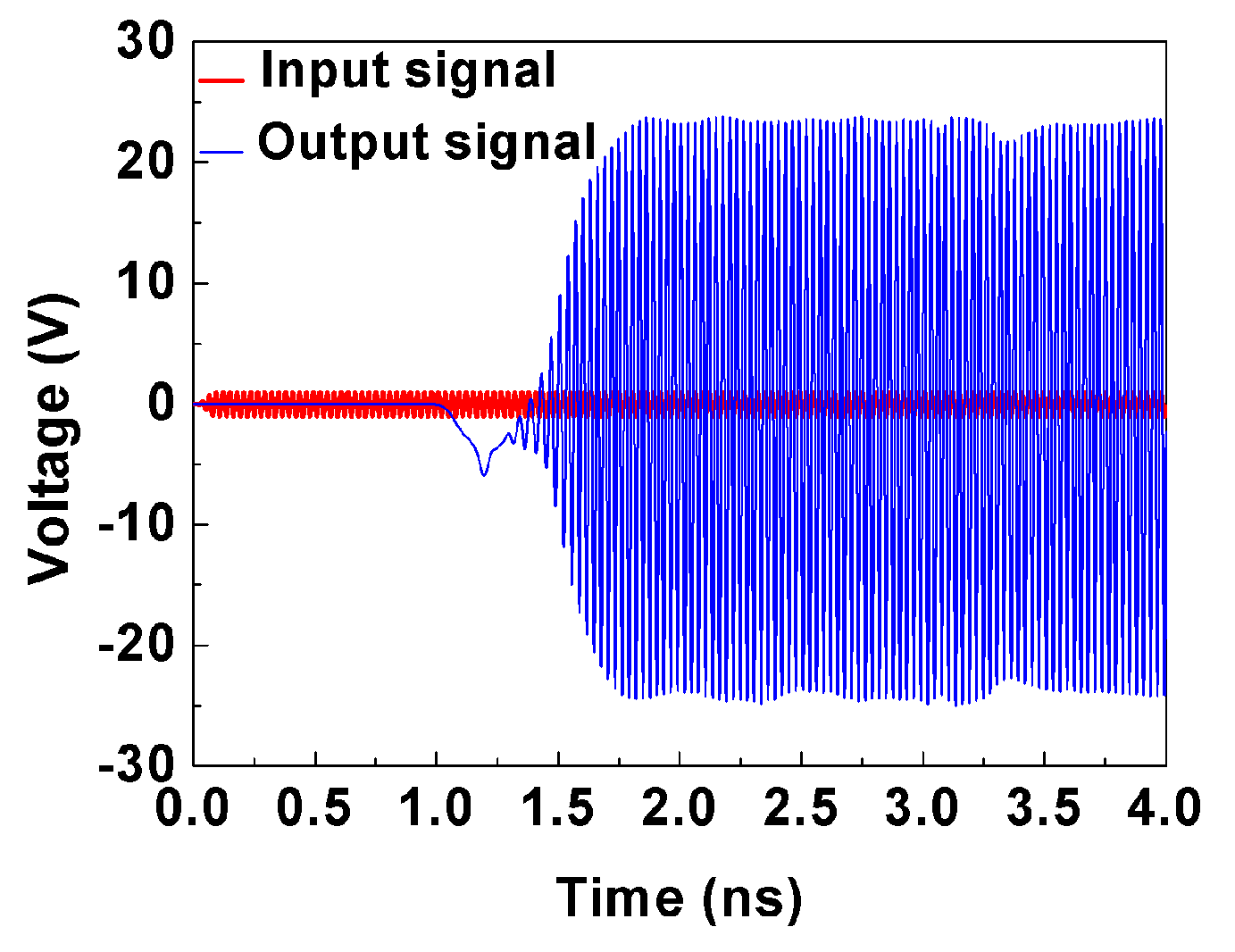
Figure 7.
Input and output signals plot of the novel amplifier at 35 GHz.
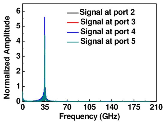
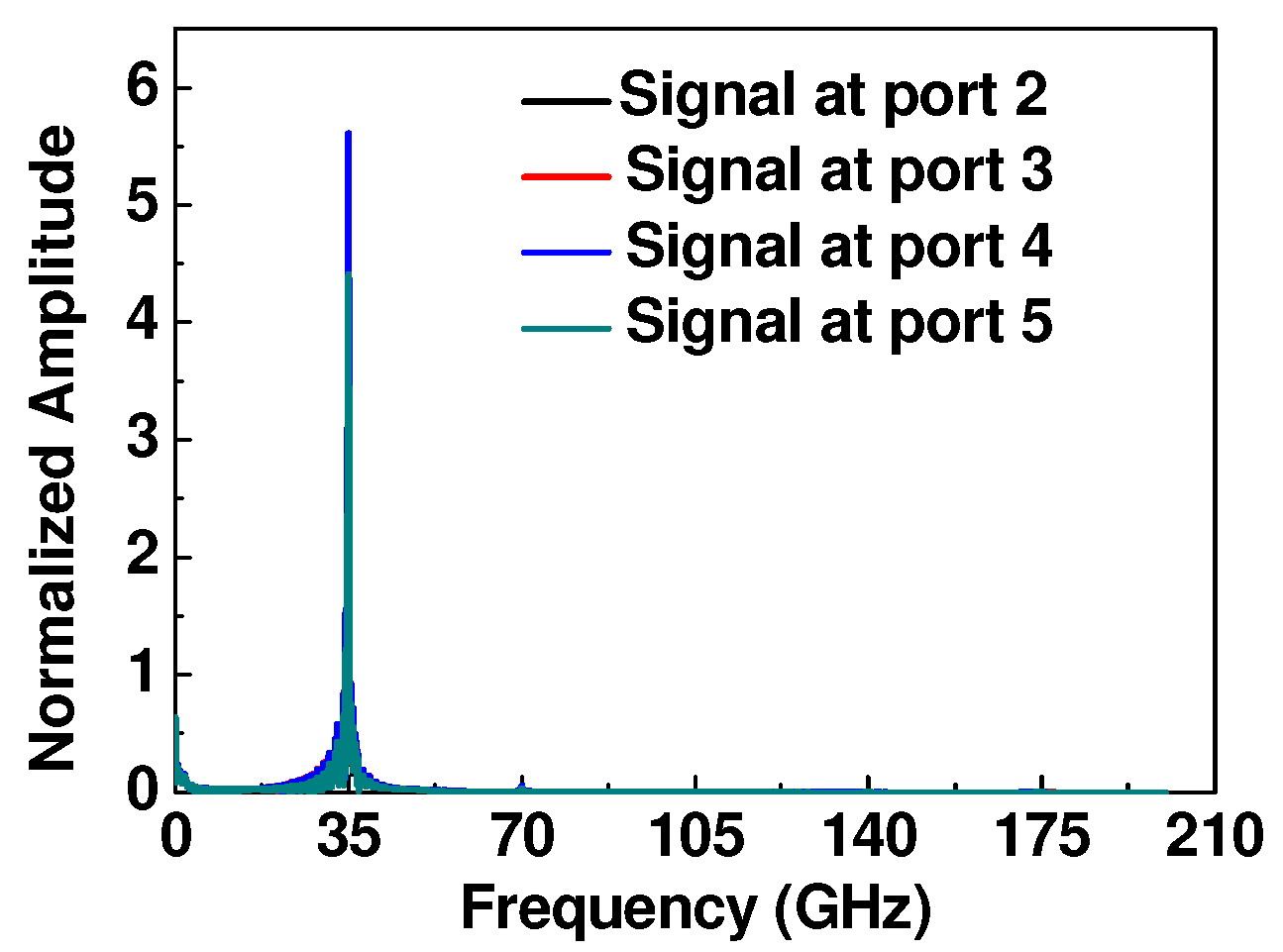
Figure 8.
Spectrums of the signals plot of the four output ports.
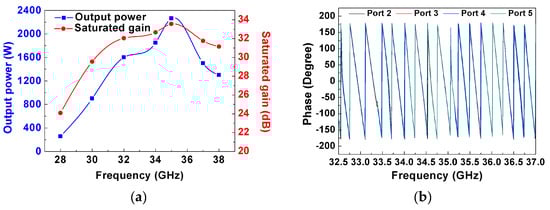
Figure 9.
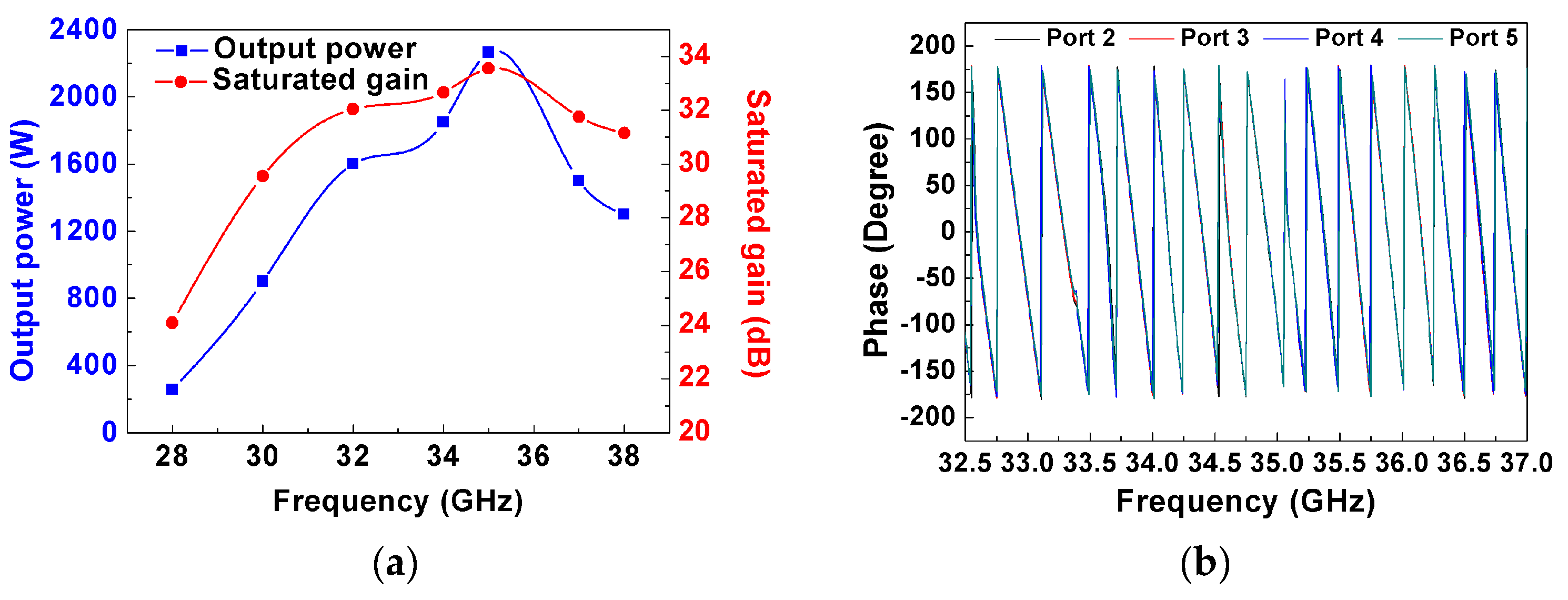
Plots of the simulated output power: the saturated gain (a); the phase congruency (b) for four output ports versus frequency.
Figure 6 shows the electron kinetic energy versus longitudinal distance when the electron dynamic system has been in steady state. As most of the electrons are decelerated at the end of the circuit, most kinetic energy from the sheet beam is transferred to electromagnetic fields and the excitation signal is amplified.
Figure 7 shows the signal amplitudes of the input port and one of the four output ports. The output signals become stable after a transient time about 1.6 ns. With the energy transfer from the electron beam to the high-frequency field, the input signal with the amplitude of 1 V is amplified to 23.8 V for a single amplifier channel, with the gains more than 27.5 dB. The signal amplitude differences of the four output ports are less than 5% according to our simulations. Therefore, the total gains for the whole 2 × 2 amplifier unit are around 33.5 dB.
As can be seen in Figure 8, the output signal spectrums are concentrated at around 35 GHz and relatively pure. The normalized amplitudes at the frequency points of 35 GHz, 70 GHz, and 105 GHz are 5.62, 0.04, and 0.0006, respectively. Due to the optimization of attenuators, no obvious backward-wave oscillation from higher order modes is observed.
The sum of the average output power of the four output ports and the saturated gain versus frequency of the amplifier according to the simulation results at a frequency of 35 GHz are 2260 W and 33.5 dB, respectively, as shown in Figure 9a. The instantaneous 3-dB bandwidth of the 2 × 2 amplifier units is 7 GHz, which demonstrates that it can maintain the broadband advantage of the MML SWS TWT.
The phase congruency for the four output port signals is investigated for its PAR applications. From the phase analysis results in CST shown in Figure 9b, we can see the phase differences among the four channels are below 5%. It indicates the great phase congruency for different channels.
4. Fabrication and Experimental Test
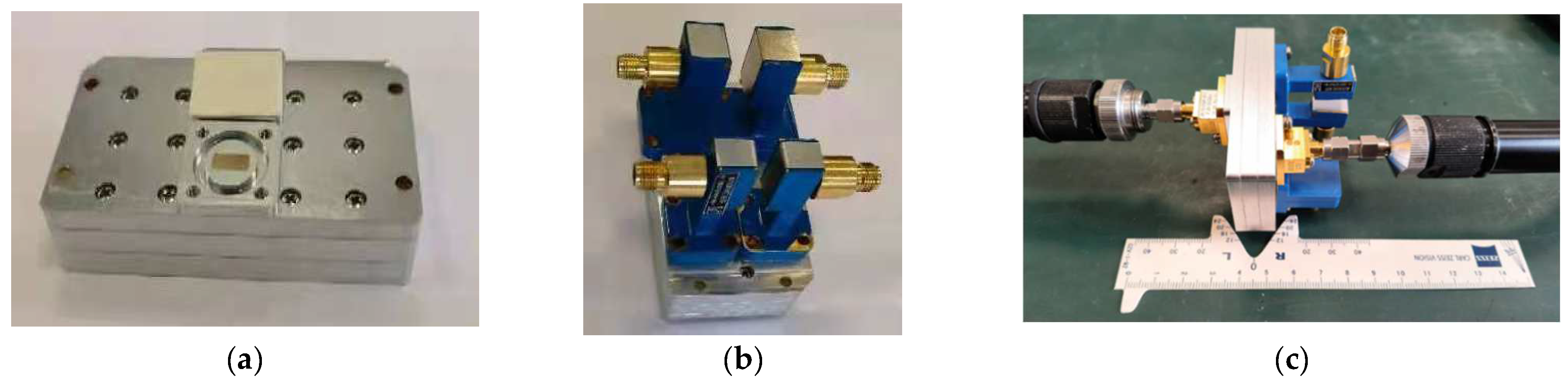
The “cold” transmission model with 80-period SWS is fabricated and tested to verify the transmission performances preliminarily. Rogers RT5880 is employed as the material of the dielectric substrates. The cavity is designed as a two-halves structure, in which the SWSs are located on the upper and lower slots. As shown in Figure 10a,b, an input waveguide port is on one side of the cavity and four coaxial cable output ports are located on another side. The dimensions of the amplifier are shown in Figure 10c.

Figure 10.
Fabricated cavity for the transmission model with the input port at the front (a); the output ports at the back (b); the dimensions (c).
Without being driven by the electron beam and input signals, only the “cold” transmission performances of the fabricated 80-period SWS in the cavity are experimentally tested preliminarily by the vector network analyzer. The S-parameters are tested when all other ports are connected with matched loads. The comparisons of the simulated values and the tested values are shown in Figure 11a,b. As shown in Figure 11a, the tested S11 values are almost below −15 dB, which is basically consistent with the simulation results. It can be seen in Figure 11b that the tested “cold” transmission loss values are around 7.5 dB, which are 0.5 dB more than the simulation values. The larger loss may be due to assembly errors.
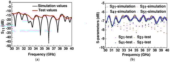
Figure 11.
Comparison between simulation values and test values for S11 parameters (a); transmission losses (b).
5. Conclusions and Discussion
This novel amplifier can probably break the traditional “one TWT for one channel” framework in PAR application. Driven by only one sheet electron beam and one input signal, four independent output signals are generated with more than 2000 W saturated peak power and 7 GHz bandwidth according to the simulation results. The phase congruency among the four output channels is also great. Moreover, this compact framework is easy to integrate with solid-state circuits. The advantages can be summarized as high power, broad bandwidth, good integrability, compact structure, and great phase congruency. Based on the analysis above, it can be concluded that this novel 2 × 2 TWT amplifier unit is promising on the millimeter wave T/R modules of the PARs. Finally, the transmission model is fabricated, and the “cold” transmission performances are tested to show the practicability of this novel amplifier.
Compared with the Ka-band GaAs power amplifier shown in reference [5], the amplifier can supply higher peak output power (2000 W vs. 4 W), higher peak gain (33.5 dB vs. 22 dB) and wider 3-dB bandwidth (7 GHz vs. 5 GHz) according to the simulation results. Compared with the MML TWT power amplifier shown in reference [11,12,13], the amplifier can supply multi-channel output signals and favorable phase congruency between channels, and thus is more suitable for the PAR applications.
However, there are still some practical issues that need to be discussed. Firstly, the preliminary tests mainly focus on the “cold” S-parameters without an electron beam. The electron gun and focus magnetic field will be considered in the next experimental step. Secondly, as a novel type of vacuum electronic device, the limited range of the working environment is still vacuum condition, so the vacuum treatment needs further research. Thirdly, due to the large power delivery, the thermal dissipation structures should be designed specially in applications.
Author Contributions
Conceptualization, G.G. and Y.W.; methodology, J.L.; software, Z.S.; validation, Z.Y. and Z.S.; writing—original draft preparation, R.Y.; writing—review and editing, G.G.; visualization, R.Y.; supervision, Y.G.; project administration, Y.W.; funding acquisition, G.G. All authors have read and agreed to the published version of the manuscript.
Funding
This work was supported in part by the Fundamental Research Funds for the Central Universities under Grant No. ZYGX2018J032, in part by the National Natural Science Foundation of China (Grant No. 61801088, 92163204, 61921002) and in part by the National Key R&D Program of China, contract numbers 2017YFE0300200 and 2017YFE0300201.
Data Availability Statement
The data presented in this study are available on request from the corresponding author.
Conflicts of Interest
The authors declare no conflict of interest.
References
- Bil, R.; Holpp, W. Modern Phased Array Radar Systems in Germany. In Proceedings of the 2016 IEEE International Symposium on Phased Array Systems and Technology(PAST), Waltham, MA, USA, 18–21 October 2016; pp. 1–7. [Google Scholar]
- Herd, J.; Carlson, D.; Duffy, S.; Weber, M.; Brigham, G.; Rachlin, M.; Cursio, D.; Liss, C.; Weigand, C. Multifunction Phased Array Radar (MPAR) for Aircraft and Weather Surveillance. In Proceedings of the 2010 IEEE Radar Conference, Arlington, VA, USA, 10–14 May 2010; pp. 945–948. [Google Scholar]
- Turlington, T.R.; Sacks, F.E.; Gipprich, J.W. T/R Module Architectural Consideration for Active Electronically Steerable Arrays. In Proceedings of the 1992 IEEE MTT-S Microwave Symposium Digest, Albuquerque, NM, USA, 1–5 June 1992; Volume 3, pp. 1523–1526. [Google Scholar]
- Turlington, T.R. Additive Functions Provide a Powerful Tool for T/R Module Modeling. In Proceedings of the 2007 IEEE Radar Conference, Boston, MA, USA, 17–20 April 2007; pp. 954–959. [Google Scholar]
- Colomb, F.Y.; Platzker, A. 2 and 4 watt Ka-band GaAs PHEMT power amplifier MMICs. In Proceedings of the IEEE MTT-S International Microwave Symposium Digest, Philadelphia, PA, USA, 8–13 June 2003; Volume 2, pp. 843–846. [Google Scholar]
- Pelk, M.J.; Neo, W.C.E.; Gajadharsing, J.R.; Pengelly, R.S.; de Vreede, L.C.N. A High-Efficiency 100-W GaN Three-Way Doherty Amplifier for Base-Station Applications. IEEE Trans. Microw. Theory Tech. 2008, 56, 1582–1591. [Google Scholar] [CrossRef] [Green Version]
- Booske, J.H.; Dobbs, R.J.; Joye, C.D.; Kory, C.L.; Neil, G.R.; Park, G.-S.; Park, J.; Temkin, R.J. Vacuum Electronic High Power Terahertz Sources. IEEE Trans. Terahertz Sci. Technol. 2011, 1, 54–75. [Google Scholar] [CrossRef]
- Baig, A.; Shin, Y.; Barnett, L.R.; Gamzina, D.; Barchfeld, R.; Domier, C.W.; Wang, J.; Luhmann, N.C., Jr.; Ieee, F. Design, Fabrication and RF Testing of Near-THz Sheet Beam TWTA. IEEE Trans. Terahertz Sci. Technol. 2011, 4, 181–207. [Google Scholar]
- Gamzina, D.; Himes, L.G.; Barchfeld, R.; Zheng, Y.; Popovic, B.K.; Paoloni, C.; Choi, E.; Luhmann, N.C. Nano-CNC Machining of Sub-THz Vacuum Electron Devices. IEEE Trans. Electron Devices 2016, 63, 4067–4073. [Google Scholar] [CrossRef]
- Shen, F.; Wei, Y.; Yin, H.; Gong, Y.; Xu, X.; Wang, S.; Wang, W.; Feng, J. A Novel V-Shaped Microstrip Meanderline Slow-Wave Structure For W-Band MMPM. IEEE Trans. Plasma Sci. 2012, 40, 463–469. [Google Scholar] [CrossRef]
- Sengele, S.; Jiang, H.; Booske, J.H.; van der Weide, D.; Kory, C.; Ives, L. A Selectively Metallized, Microfabricated W-Band Meanderline TWT Circuit. In Proceedings of the 2008 IEEE International Vacuum Electronics Conference, Monterey, CA, USA, 22–24 April 2008; pp. 447–448. [Google Scholar]
- Shen, F.; Wei, Y.Y.; Xu, X.; Liu, Y.; Huang, M.Z.; Tang, T.; Duan, Z.Y.; Gong, Y.B. Symmetric Double V-Shaped MML Slow-Wave Structure for W-Band Traveling-Wave Tube. IEEE Trans. Electron Devices 2012, 59, 1551–1557. [Google Scholar] [CrossRef]
- Nehra, A.K.; Gupta, R.K.; Panda, P.C.; Sharma, S.M.; Choyal, Y.; Sharma, R.K. Electron Gun Design for Multi-Beam Pulsed Amplifier. In Proceedings of the IEEE International Vacuum Electronics Conference, Monterey, CA, USA, 24–26 April 2012; pp. 175–176. [Google Scholar]
- Dassault Systemes. CST-Computer Simulation Technology. 2020. Available online: http://www.cst.com (accessed on 25 September 2021).

Publisher’s Note: MDPI stays neutral with regard to jurisdictional claims in published maps and institutional affiliations. |
© 2021 by the authors. Licensee MDPI, Basel, Switzerland. This article is an open access article distributed under the terms and conditions of the Creative Commons Attribution (CC BY) license (https://creativecommons.org/licenses/by/4.0/).