Article

A Quasi-Z-Source-Based Inductive Power Transfer System for Constant Current/Constant Voltage Charging Applications

by
Vincenzo Castiglia
1,*,†,
Nicola Campagna
1,†,
Rosario Miceli
1,†,
Fabio Viola
1,† and
Frede Blaabjerg
2,†
1
Department of Engineering, University of Palermo, 90128 Palermo, Italy
2
Department of Energy Technology, University of Aalborg, 9100 Aalborg, Denmark
*
Author to whom correspondence should be addressed.
All authors contributed equally to this work.
Electronics 2021, 10(23), 2900; https://doi.org/10.3390/electronics10232900
Submission received: 27 October 2021 / Revised: 16 November 2021 / Accepted: 18 November 2021 / Published: 24 November 2021
(This article belongs to the Special Issue Battery Chargers and Management for Electric Vehicles)

Abstract

:
This article proposes a quasi-Z-source (qZS)-based Inductive Power Transfer (IPT) system for Electric Vehicles (EVs) charging applications. The IPT systems use the magnetic field to transfer power between two coils wirelessly, achieving improved reliability, safety and less environmental impact. Compared to the conventional IPT system, the proposed qZS-IPT system simultaneously achieves DC/DC regulation and DC/AC conversion through a single-stage conversion, thus lowering the cost and complexity of the system. Moreover, the reliability of the system is improved thanks to the qZS network shoot-though immunity and the reduced number of switches. To ensure the battery efficient charging and long service life, the constant current/constant voltage (CC/CV) method is considered. With the proposed innovative modulation scheme, the qZS can easily change between buck and boost modes, respectively, lowering or increasing the secondary side current. A theoretical analysis is presented for system design. Simulation results based on a 25 kW (200 V/135 A) low duty EV charger are presented to verify the effectiveness of the proposed scheme. Experimental tests are performed on a 150 W scale-down prototype to validate the analysis and demonstrate the effectiveness of the proposed qZS-IPT system for CC/CV chargers.

1. Introduction

The growing need to reduce polluting emissions leads, in our days, to the rapid spread of Electric Vehicles (EVs) [1]. Thanks to high-performance electric motors and the use of “clean” energy sources for recharging EVs, the contribution of polluting gases caused by transportation could be drastically reduced. One of the most discussed topics in this area is the EVs charging mode [2,3,4,5]. Two different connection methods have been proposed for recharging the EVs: the classic one, which provides a cable connection (conductive or wired charging) [6], and the innovative one involving wireless power transmission (wireless charging) [7]. Wireless Power Transfer (WPT) systems use the electric field (Capacitive Power Transfer, CPT) [8,9,10] or magnetic field (Inductive Power Transfer, IPT) [11,12,13] to transfer power from a primary side to a secondary side. By removing the connection cable between the charging station and EV, the electrocution hazard is eliminated, the risk of short circuits and sparks is reduced, contact resistors are eliminated and the possibility of contact failures or breakage is then eliminated. Moreover, WPT systems are also unaffected by dirt, dust, and water. Thus, compared to wired systems, improved reliability, safety and less environmental impact are achieved [14].
The IPT systems have been preferred over CPT systems and have been developed and commercialized rapidly [15,16]. The general architecture of an IPT system for EV charging applications is shown in Figure 1 [17,18]. It consists of two sides, respectively, the transmitter side located in the charging station and the receiving side located in the vehicle. The charging station can be supplied by the grid, as shown in Figure 1, or by a DC power source such as Photovoltaic (PV) or Fuel Cells (FC). In a typical IPT system, the input voltage is usually regulated by a boost DC/DC converter. To increase the coupling between the two coils, the DC/AC in the primary side and the AC/DC converter in the secondary side must work at high frequencies, in the order of hundreds of kHz. On the other hand, to keep the system efficient, switching losses limit the operating frequencies [19].
In order to overcome this problem, a second possible configuration has been proposed using Impedance Source (Z-Source) converters [20,21,22,23,24,25,26,27]. The main advantage of using these converters is the single-stage DC/AC conversion with a smaller number of switches [28]. In fact, it is possible to obtain the DC voltage boost and AC conversion simultaneously [29,30]. Moreover, the input impedance network (Z-network) ensures short circuit protection.
Another key element in IPT systems is the battery charging method [31,32]. Lithium-ion (Li-ion) batteries are currently the most widely used in EV storage systems due to their high energy density [33,34]. The best Li-ion batteries charging method, which ensures efficient charging and long service life, is the constant current-constant voltage (CC/CV) [14] method. Different solutions have been adopted for the CC/CV charge implementation [35]. In [36], two different control loop are used to achieve the CC mode and the CV mode, measuring the battery voltage and current and controlling only the primary side inverter. In [37], a load identification approach is used to avoid the battery voltage and current sensing and the data communication between the primary and secondary side. In [38], the CC and CV modes are implemented using a reconfigurable IPT system. In [39], a decoupled control method is proposed, which enhances the transient response and the overall system performance compared to the traditional closed-loop control. It should be noted that the articles reviewed so far are all preferred for the classic IPT configuration, while there are still few works that consider the implementation of the CC/CV charging mode on Z-source converters-based IPT systems.
In [22,26], a Z-source converter with integrated Power Factor Correction (PFC) and load regulation for sinusoidal charging of batteries is proposed. The main problem of the Z-source converter is the discontinuous input current, which is not very suitable for renewable energy sources like PV and FCs. To achieve a continuous input current, the quasi-Z-source (qZS) converter is used in [20,27]. In [20], the performance comparison of the qZS and Z-source converters is carried out. In [27], the sliding mode predictive control is applied to the qZS converter, but the charging process of batteries is not taken into account. In [21], the qZS converter is controlled in the CC/CV mode to recharge the batteries, using two separated control schemes and a buck converter in the receiver side.
With the above, the main motivation of this article is to investigate impedance source converters in IPT systems for CC/CV charging of EV batteries. Among the different Z-source converter topologies, the qZS was chosen because of the continuous input current feature. The detailed schematic of the proposed qZS based Inductive Power Transfer system (qZS-IPT) is shown in Figure 2. In contrast to the one proposed in [20,21,27], the Z-network diode is replaced by a switch to ensure the Continuous Conduction Mode (CCM) operation. The inductive coupling is realized by means of the series-series (SS) topology, which features a load independent characteristic during the CC mode. To achieve the CC/CV charging method, the control acts on the primary side qZS converter and with a proper modulation scheme, the converter can increase (boost mode) or decrease (buck mode) the voltage on the primary side. To summarize, the main contributions of this paper, compared to what is found in the literature, are underlined in the following:
  • Unlike [21], the receiver side buck converter is removed to keep the design as simple as possible;
  • Use of a single control scheme for the implementation of CC/CV phases, achieving a smooth transition between the two modes;
  • Implementation of an innovative modulation scheme that allows the qZS converter to easily change between boost and buck modes.
Figure 2. Circuit schematic of the qZS-based IPT system.
Electronics 10 02900 g002
This article has been divided into five sections. Section 2 describes the operating principle of the system and the basic theoretical analysis. Section 3 presents the CC/CV charge implementation. Section 4 describes the system operation with simulations in PLECS. A small-scale prototype is presented in Section 5 and the acquired waveforms and recorded CC/CV charging curves are provided, validating the proposed system with experimental results.

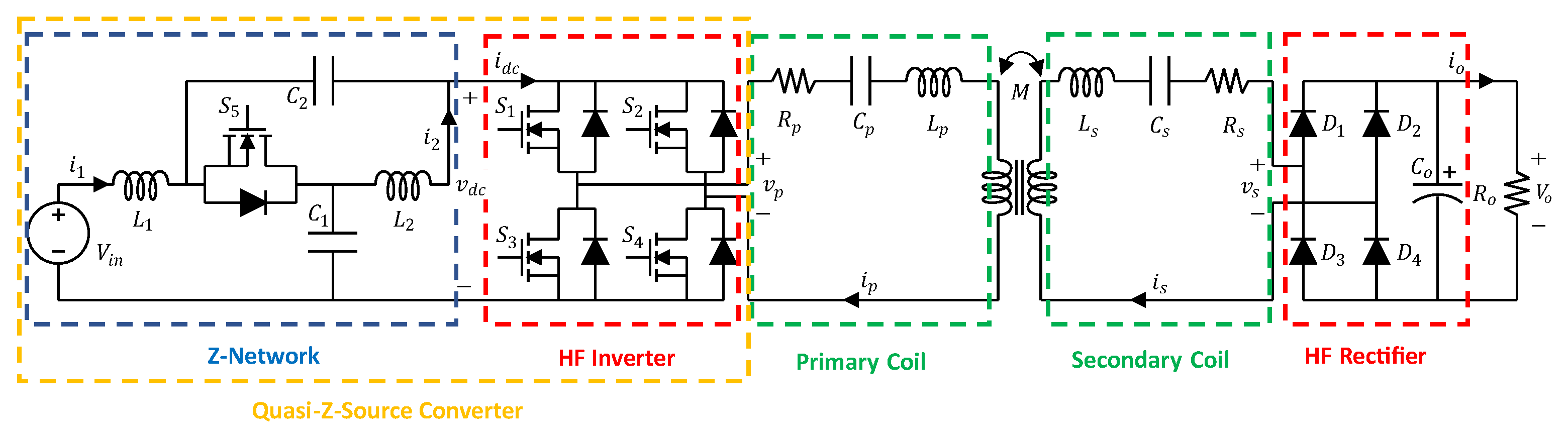
2. System Analysis and Modeling

The qZS converter has different states based on which switch is turned ON or OFF. In addition to the Active State (AS) and Zero State (ZS), normally used in traditional inverters, the Shoot-Through (ST) state is introduced. All the possible configurations of the converter are shown in Figure 3 and are described below.
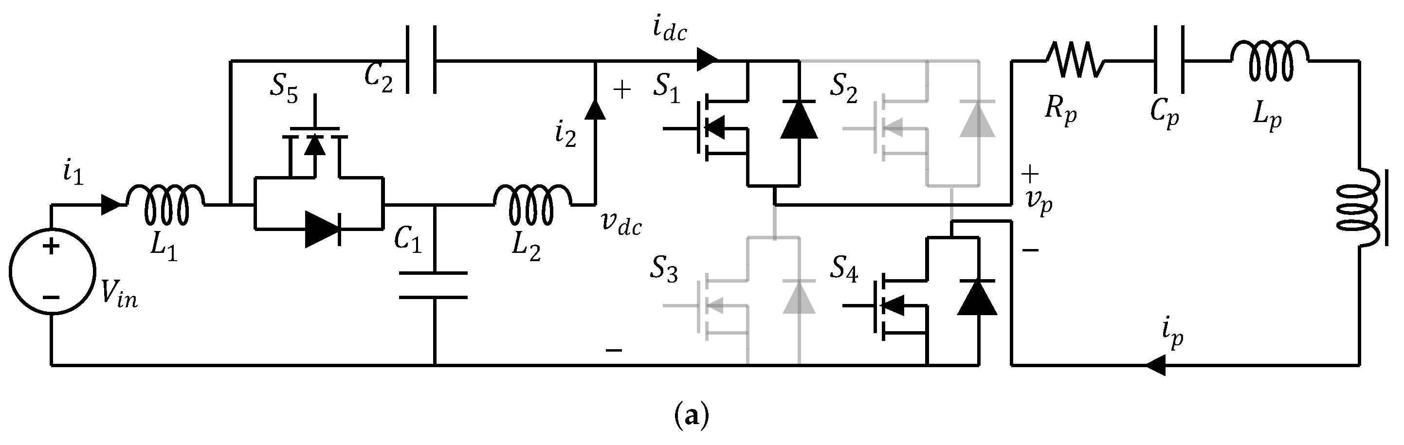
  • Active State: During the AS, the diagonal switches ( S 1 and S 4 or S 2 and S 3 ) are ON and the switch S 5 is ON (see Figure 3a,b). The capacitors C 1 and C 2 are connected in series through S 5 and supply current to the load along with the DC source.
  • Zero State: During the ZS, the upper ( S 1 and S 2 ) or lower ( S 3 and S 4 ) switches are ON and the switch S 5 is ON (see Figure 3c,d). The transmitter current is freewheeling, the Z-network inductors and the source charge the Z-network capacitors.
  • Shoot-Through State: During the ST state, the switches S 1 to S 4 are ON and S 5 is OFF (see Figure 3e). The inductors are charged both by the DC source and the Z-network capacitors. Thanks to this ST state, the Z-network output voltage is boosted. Using the voltage-second balance across one of the Z-network inductors, the DC-link peak voltage can be obtained as:
    v ^ D C = 1 1 2 D V i n
    where D is the duty cycle.
Combining the previous three states, different operating modes can be achieved. In particular, the system can operate both in boost mode, increasing the DC-link voltage with respect to the input voltage, in buck mode, decreasing the AC output voltage or in buck-boost mode.

2.1. Buck Mode

In buck mode operation, only the AS and ZS are used.
The first harmonic of the inverter output voltage, denoted with v p , 1 , can be expressed as:
v p , 1 = 4 V D C π cos π 2 D sin ω 0 t .
The DC-link voltage V D C during the buck mode operation is equal, neglecting the voltage drops across the Z-network components to:
V D C V i n
thus, the amplitude of the first harmonic is:
v ^ p , 1 = 4 V i n π cos π 2 D
and it will be maximum when the duty cycle is 0 and minimum when the duty cycle is 1. The output current in this operation mode can be calculated as:
I o = 8 ω 0 M V i n π 2 cos π 2 D .

2.2. Boost Mode

In boost mode operation, only the AS and the ST state are used. The inverter output voltage first harmonic expression is the same in (2). However, thanks to the boosting action during the ST state, the DC-link peak voltage will be increased as reported in (1). Thus, the amplitude of the first harmonic during the boost mode can be calculated, replacing (1) in (2) as:
v ^ p , 1 = 4 V i n π 1 1 2 D cos π 2 D
and it will be minimum for D equal to 0 and theoretically infinite for D equal to 0.5 .
The output current in this operation mode can be calculated as
I o = 8 V i n ω 0 M π 2 ( 1 2 D ) cos π 2 D .

2.3. Buck-Boost Mode

In order to achieve a smooth transition between buck and boost mode and to use a single modulator for both operation modes, a new control logic was implemented. In particular, the duty cycle has been allowed to vary not between 0 and 1 for the buck mode and between 0 and 0.5 for the boost mode, as normally happens, but between 1 and 0 for buck mode and between 0 and 0.5 for boost mode. In this way, when the control circuit tries to decrease the current, the duty cycle may become negative by switching to buck operation. The control signals S 1 , S 2 and S 5 are generated in the same way for both operation modes. The S 3 and S 4 signals remain to be generated differently, so we introduce a variable T that indicates whether the duty cycle is greater ( T = 0 ) or smaller ( T = 1 ) than 0. Thus, the following relationship and truth Table 1 can be written:
S 3 = S 2 , D > 0 T = 0 S 1 ¯ , D < 0 T = 1 ,
S 4 = S 1 , D > 0 T = 0 S 2 ¯ , D < 0 T = 1 .
Considering all the minterms in the truth tables, the following combinatorial expressions are obtained.
T ¯ S 1 ¯ S 2 + T ¯ S 1 S 2 + T S 1 ¯ S 2 + T S 1 ¯ S 2 ¯ = T ¯ S 1 ¯ S 2 + T ¯ S 1 S 2 + T S 1 ¯ S 2 + T S 1 ¯ S 2 ¯ = S 1 ¯ S 2 + T ¯ S 1 S 2 + T S 1 ¯ S 2 ¯
T ¯ S 1 S 2 + T ¯ S 1 S 2 ¯ + T S 1 ¯ S 2 ¯ + T S 1 S 2 ¯ = T ¯ + T S 1 S 2 ¯ + T ¯ S 1 S 2 ¯ + T S 1 ¯ S 2 ¯ = S 1 S 2 ¯ + T ¯ S 1 S 2 ¯ + T S 1 ¯ S 2 ¯
The combinational logic circuit associated to (10) and (11) is shown in Figure 4. This circuit is implemented in the FPGA-based control board to realize the PWM modulator.

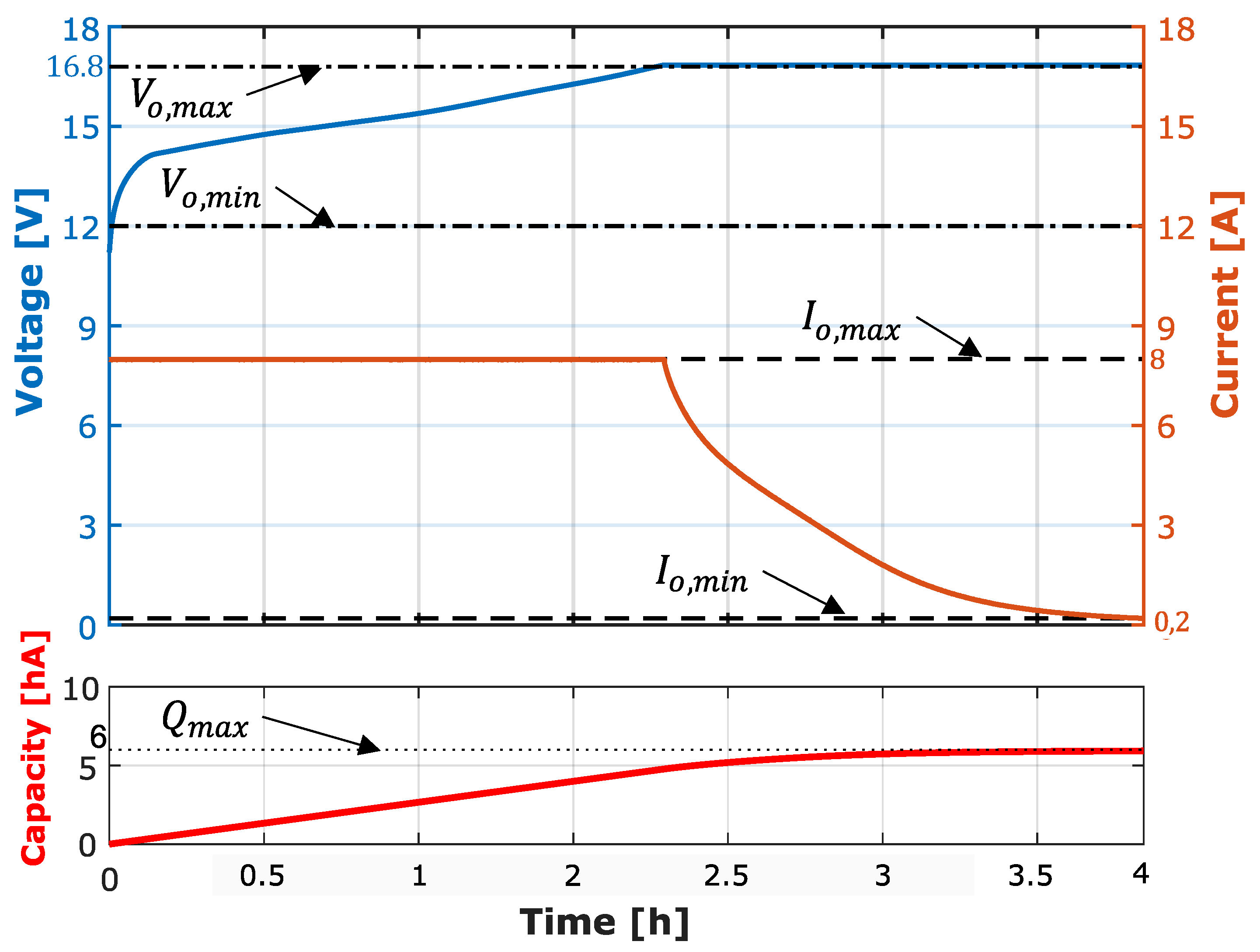
3. CC/CV Charging Implementation

In order to ensure fast and safe charging of the battery, the CC/CV charging method was considered. It consists of two phases: in the CC phase, the battery charging current is kept constant and equal to I m a x until the battery voltage reaches its maximum allowable value V m a x .
In the CV phase, the battery voltage is kept constant to V m a x until the battery charge current reaches a minimum value I m i n .
The CC/CV charge was implemented using a double-loop control scheme: the external loop, which controls the battery voltage V o , and the internal loop which controls the battery current I o . An interesting feature of the proposed control method is the possibility to achieve a smooth transition between CC and CV charging modes, with no need to reconfigure the controller. The complete control scheme is shown in Figure 5.
The battery voltage V o is measured and compared to the reference value V o * , set to the maximum allowable voltage for the battery. The error is sent to a Proportional-Integral (PI) controller to generate the reference charging current I o * , which is compared to the actual battery current I o and processed by the second PI controller to generate the reference duty cycle D * . To the first PI controller output, a saturation block is added. The upper limit of the saturation block is set to be equal to the maximum battery charging current, while the lower limit is set to 0.
To the second PI controller output, another saturation block is added to limit the duty cycle, with the upper saturation limit set to 0.4 and the lower saturation limit set to 1 . In this way, when the battery voltage is low, the PI controller tries to increase the charging current, which will be saturated to the maximum permissible value by the battery. During the CC phase, the converter usually works in boost mode, with duty cycle in the range of 0 to 0.4 . As the battery charges, the charging current will be kept constant until the maximum voltage is reached. At this point, the system automatically switches to the CV phase, during which the charging current is reduced to a minimum value. In this phase, the converter will switch to the buck mode when the duty cycle becomes negative in the range of 0 to 1 . When the charging current reaches the minimum value, the charging process is completed.

4. Simulation Results

The proposed system was designed and simulated in PLECS. The simulation parameters are summarized in Table 2. The simulation is carried out to demonstrate the system behaviour during the CC-CV charge. Figure 6 shows the steady- state voltage and current waveforms during boost mode (a) and buck mode (b) operation of each stage of the proposed system. From top to bottom the input voltage V i n and current i 1 , the DC-link voltage v D C and current i D C , the primary side voltage v p and current i p , the secondary side voltage v s and current i s and the battery voltage V o and current I o are represented.
Figure 6a shows the waveforms during boost mode and CC phase. The battery charging current reference is set to 125 A (red dashed line), corresponding to a duty cycle of 0.18 . During the shoot-though state, the DC-link current reaches almost 200 A, charging the Z-network inductors. It can be noticed that the DC-link voltage is boosted from 330 V to almost 500 V.
Figure 6b shows the waveforms during buck mode and CV phase. The battery maximum voltage reference is set to 225 V, corresponding to a duty cycle of 0.57 . It can be noticed that the DC-link voltage in this case is practically constant and equal to the input voltage apart from voltage drops on components.
In CC phase, the closed-loop control maintains the battery charging current to 125 A while the battery voltage is increasing. As the battery voltage reaches the maximum value V o , m a x = 225 V, the CV phase is activated. To maintain a constant voltage, the charging current is proportionally decreased until its value reaches the minimum battery charging current I o , m i n = 5 A. Thanks to the improved control algorithm, no voltage and current transients are observed during the transition from CC to CV phase.

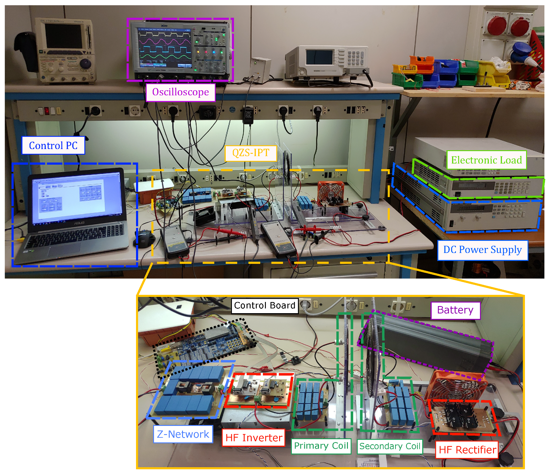
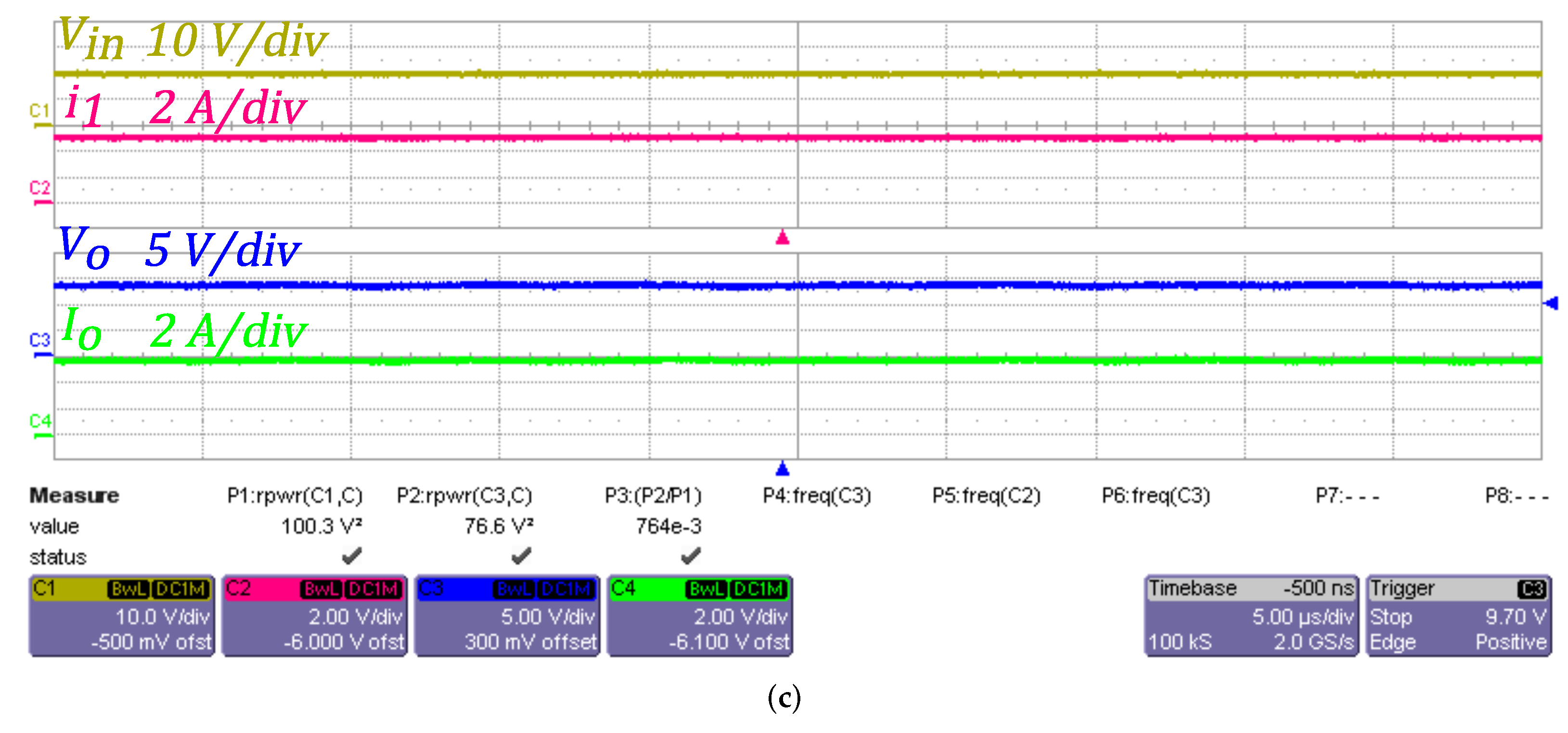
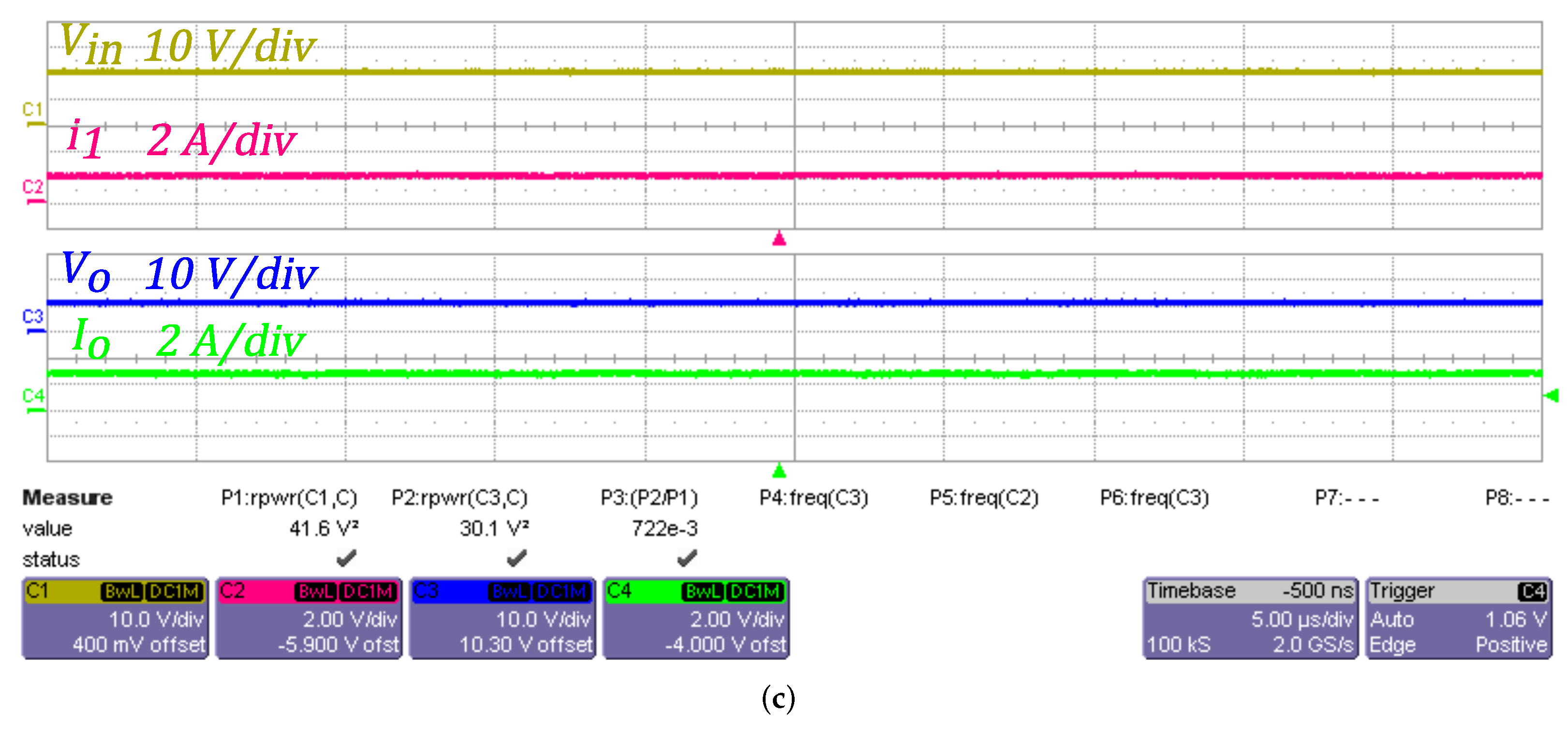
5. Experimental Results

Experimental tests have been performed on a scaled-down prototype to validate the simulation results and prove that the system achieves the CC-CV charge. The test-bench, shown in Figure 7, is composed of:
  • A PED-board, used to acquire voltages and currents, implement the control algorithm and generate the control signals for the inverter;
  • The proposed qZS-IPT system, whose parameters are summarized in Table 3;
  • An Agilent 6672A DC Power Supply (0–20 V/0–100 A, 2 kW), used as the input source;
  • An Agilent 6060B Single Input Electronic Load (3–60 V/0–60 A, 300 W), used as a load in voltage mode for open-loop tests;
  • A lithium-ion battery, whose parameters are reported in Table 4, used for the CC-CV charging demonstration;
  • A Lecroy WavePro 7200A oscilloscope with two differential voltage probe and two current probe.
Figure 7. Setup of the laboratory prototype for the proposed qZS-IPT system.
Electronics 10 02900 g007
Figure 8, Figure 9, Figure 10 and Figure 11 show the key waveforms of the proposed system in open-loop configuration with the electronic load, in voltage mode, set to 12 V. A critical aspect of the experimental realization of the laboratory prototype is the lack of a proper DC-link capacitor to suppress the sharp transients and possible overvoltage due to high di/dt. For this reason, in order to protect the power switches, a RC snubber circuit is used, in parallel to each inverter MOSFET.
Figure 8 and Figure 9 show the waveforms obtained in boost mode, with D = 0.1 and D = 0.2 , respectively. Figure 8a and Figure 9a show the Z-network input and output voltage and current. The theoretical DC-link peak voltage can be calculated using (1), obtaining 25 V for D = 0.1 and 33 V for D = 0.2 . The practical DC-link peak voltage was 22 V and 30 V, respectively, due to the component voltage drops. Figure 8b and Figure 9b show the inverter output voltage and current and the rectifier input voltage and current. The theoretical secondary current is equal to 9.8 A for D = 0.1 and 12.6 A for D = 0.2 . The practical secondary current amplitude was 9.2 A and 12 A. Figure 8c and Figure 9c show the input and output voltage and current. The theoretical output current value can be calculated by using (7) to be 6.25 A for D = 0.1 and 8 A for D = 0.2 . The measured value was 5.9 A and 7.6 A, respectively.
Figure 10 and Figure 11 report the key waveforms of the system in buck mode operation obtained with D = 0.2 and D = 0.4 , respectively. Figure 10a and Figure 11a show the Z-network input and output voltage and current. As expected, the DC-link voltage in this case is constant and equal to the input voltage, hence 20 V. Figure 10b and Figure 11b show the inverter output voltage and current and the rectifier input voltage and current. The theoretical secondary current amplitude is equal to 7.5 A for D = 0.2 and 6.4 A for D = 0.4 . The practical secondary current amplitude was 7 A and 6 A. Figure 10c and Figure 11c show the input and output voltage and current. The theoretical output current value can be calculated by using (4) to be 4.4 A for D = 0.2 and 3.77 A for D = 0.4 . The measured value was 3.9 A and 3.2 A, respectively.
The experimental results are in accordance with the mathematical analysis carried out in Section 2, demonstrating the correct operation of the modulator by switching from boost operation, for positive duty cycle values, to buck operation, for negative duty cycle values. Moreover, the measured values of voltages and currents in the various stages of the system agree with the theoretical ones, demonstrating the correct operation of the prototype.
To demonstrate the CC/CV charge process for the proposed system, the control scheme shown in Figure 5 was implemented in the control board, using LabVIEW. The control board interfaces with a control PC, on which a graphic interface has been realized to control the various parameters of the system. The battery was first discharged to the minimum voltage V o , m i n = 12 V and was then connected to the qZS-IPT system. The maximum current for the CC phase was set to I o , m a x = 8 A, the maximum voltage for the CV phase was set to V o , m a x = 16.8 V and the minimum current to stop the charging process was set to I o , m i n = 0.2 A. Figure 12 shows the acquired battery voltage and current during the entire process and the estimated capacity using the Coulomb counting method. As predicted by the simulations, the system was able to perform CC/CV charging, without transients during the transition between the two phases.

6. Conclusions

This article has presented a quasi-Z-source-based IPT system for EV battery charging applications. Thanks to the Z-network the qZS-IPT system is immune to short-circuiting and taking advantage of the shoot-through states the simultaneous DC voltage regulation and DC/AC conversion is possible. A new modulator has been proposed, capable of making the transition between buck and boost modes in a simple and effective way. Among the different charging methods, the CC/CV charge was chosen. Unlike many other papers that propose two separate control loops, one for the CC phase and one for the CV phase, a single double-loop control was proposed improving the transition between the two phases This article validated the theoretical analysis by means of simulations and experimental results, verifying proper system operation in both buck and boost modes, and ensuring the system ability to perform CC/CV charging.

Author Contributions

All authors (V.C., N.C., R.M., F.V. and F.B.) contributed equally to this work. Conceptualization, V.C. and N.C.; methodology, V.C. and N.C.; software, V.C.; validation N.C.; writing—review and editing, F.V.; supervision, R.M. and F.B.; project administration R.M. and F.V. All authors have read and agreed to the published version of the manuscript.

Funding

This work was financially supported by PON R&I 2015–2020 “Propulsione e Sistemi Ibridi per velivoli ad ala fissa e rotante—PROSIB”, CUP no:B66C18000290005, by H2020-ECSEL-2017-1-IA-two-stage, by “first and european sic eightinches pilot line-REACTION”, by Prin 2017- Settore/Ambito di intervento: PE7 linea C—Advanced power-trains and -systems for full electric aircrafts, by PON R&I 2014–2020—AIM (Attraction and International Mobility), project AIM1851228-1.

Conflicts of Interest

The authors declare no conflict of interest.

Abbreviations

The following abbreviations are used in this manuscript:
V i n [V]input voltage
i 1 [A]input current
L 1 , L 2 [H]Z-network inductors
C 1 , C 2 [F]Z-network capacitors
v d c [V]DC-link voltage
i d c [A]DC-link current
S 1 S 5 qZS converter switches
v p [V]Primary side voltage
i p [A]Primary side current
L p [H]Primary self-inductance
C p [F]Primary compensation capacitor
R p [ Ω ]Primary coil resistance
M [H]Mutual inductance
L s [H]Secondary self-inductance
C s [F]Secondary compensation capacitor
R s [ Ω ]Secondary coil resistance
v s [V]Secondary side voltage
i s [A]Secondary side current
D 1 D 4 Rectifier diodes
C o [F]Output capacitor
R o [ Ω ]Load resistance
V o [V]Output voltage
I o [A]Output current

References

  1. Liao, Y.T.; Lu, C.N. Dispatch of EV Charging Station Energy Resources for Sustainable Mobility. IEEE Trans. Transp. Electrif. 2015, 1, 86–93. [Google Scholar] [CrossRef]
  2. Khaligh, A.; Li, Z. Battery, Ultracapacitor, Fuel Cell, and Hybrid Energy Storage Systems for Electric, Hybrid Electric, Fuel Cell, and Plug-In Hybrid Electric Vehicles: State of the Art. IEEE Trans. Veh. Technol. 2010, 59, 2806–2814. [Google Scholar] [CrossRef]
  3. Li, S.; Mi, C.C. Wireless Power Transfer for Electric Vehicle Applications. IEEE J. Emerg. Sel. Top. Power Electron. 2015, 3, 4–17. [Google Scholar] [CrossRef]
  4. Márquez-Fernández, F.J.; Bischoff, J.; Domingues-Olavarría, G.; Alaküla, M. Assessment of future EV charging infrastructure scenarios for long-distance transport in Sweden. IEEE Trans. Transp. Electr. 2021. [Google Scholar] [CrossRef]
  5. Chan, C.C. The State of the Art of Electric, Hybrid, and Fuel Cell Vehicles. Proc. IEEE 2007, 95, 704–718. [Google Scholar] [CrossRef]
  6. He, P.; Khaligh, A. Comprehensive Analyses and Comparison of 1 kW Isolated DC–DC Converters for Bidirectional EV Charging Systems. IEEE Trans. Transp. Electrif. 2017, 3, 147–156. [Google Scholar] [CrossRef]
  7. Patil, D.; McDonough, M.K.; Miller, J.M.; Fahimi, B.; Balsara, P.T. Wireless Power Transfer for Vehicular Applications: Overview and Challenges. IEEE Trans. Transp. Electrif. 2018, 4, 3–37. [Google Scholar] [CrossRef]
  8. Vincent, D.; Huynh, P.S.; Azeez, N.A.; Patnaik, L.; Williamson, S.S. Evolution of Hybrid Inductive and Capacitive AC Links for Wireless EV Charging—A Comparative Overview. IEEE Trans. Transp. Electrif. 2019, 5, 1060–1077. [Google Scholar] [CrossRef]
  9. Lu, F.; Zhang, H.; Hofmann, H.; Mi, C. A Double-Sided LCLC-Compensated Capacitive Power Transfer System for Electric Vehicle Charging. IEEE Trans. Power Electron. 2015, 30, 6011–6014. [Google Scholar] [CrossRef]
  10. Theodoridis, M.P. Effective Capacitive Power Transfer. IEEE Trans. Power Electron. 2012, 27, 4906–4913. [Google Scholar] [CrossRef]
  11. Zhong, W.; Hui, S.Y.R. Maximum Energy Efficiency Operation of Series-Series Resonant Wireless Power Transfer Systems Using On-Off Keying Modulation. IEEE Trans. Power Electron. 2018, 33, 3595–3603. [Google Scholar] [CrossRef]
  12. Liu, J.; Chan, K.W.; Chung, C.Y.; Chan, N.H.L.; Liu, M.; Xu, W. Single-Stage Wireless-Power-Transfer Resonant Converter With Boost Bridgeless Power-Factor-Correction Rectifier. IEEE Trans. Ind. Electron. 2018, 65, 2145–2155. [Google Scholar] [CrossRef]
  13. Li, H.; Wang, K.; Fang, J.; Tang, Y. Pulse Density Modulated ZVS Full-Bridge Converters for Wireless Power Transfer Systems. IEEE Trans. Power Electron. 2019, 34, 369–377. [Google Scholar] [CrossRef]
  14. Yilmaz, M.; Krein, P.T. Review of Battery Charger Topologies, Charging Power Levels, and Infrastructure for Plug-In Electric and Hybrid Vehicles. IEEE Trans. Power Electron. 2013, 28, 2151–2169. [Google Scholar] [CrossRef]
  15. Esteban, B.; Sid-Ahmed, M.; Kar, N.C. A Comparative Study of Power Supply Architectures in Wireless EV Charging Systems. IEEE Trans. Power Electron. 2015, 30, 6408–6422. [Google Scholar] [CrossRef]
  16. Ahmad, A.; Alam, M.S.; Chabaan, R. A Comprehensive Review of Wireless Charging Technologies for Electric Vehicles. IEEE Trans. Transp. Electrif. 2018, 4, 38–63. [Google Scholar] [CrossRef]
  17. Feng, H.; Tavakoli, R.; Onar, O.C.; Pantic, Z. Advances in High-Power Wireless Charging Systems: Overview and Design Considerations. IEEE Trans. Transp. Electrif. 2020, 6, 886–919. [Google Scholar] [CrossRef]
  18. Mohammad, M.; Onar, O.C.; Su, G.J.; Pries, J.; Galigekere, V.P.; Anwar, S.; Asa, E.; Wilkins, J.; Wiles, R.; White, C.P.; et al. Bidirectional LCC-LCC Compensated 20 kW Wireless Power Transfer System for Medium-Duty Vehicle Charging. IEEE Trans. Transp. Electr. 2021. [Google Scholar] [CrossRef]
  19. Wang, C.-S.; Stielau, O.H.; Covic, G.A. Design considerations for a contactless electric vehicle battery charger. IEEE Trans. Ind. Electron. 2005, 52, 1308–1314. [Google Scholar] [CrossRef]
  20. Mahdavi, M.S.; Gharehpetian, G.B. A New Wireless Power Transfer Topology based on Quasi-Z-Source and LLC Resonant Network with Low Input Current THD. In Proceedings of the 2019 10th International Power Electronics, Drive Systems and Technologies Conference (PEDSTC), Shiraz, Iran, 12–14 February 2019; pp. 373–376. [Google Scholar] [CrossRef]
  21. Iqbal, A.; Al-Hitmi, M.A.; Maroti, P.K.; Daula, M.; Meraj, M.; Rahman, S. A Quasi Impedance Source Inverter based Wireless Power Transfer System for Battery Charging Applications for Electric Vehicle. In Proceedings of the 2019 International Conference on Electrical, Electronics and Computer Engineering (UPCON), Aligarh, India, 8–10 November 2019; pp. 1–6. [Google Scholar] [CrossRef]
  22. Zeng, H.; Wang, X.; Peng, F.Z. High Power Density Z-Source Resonant Wireless Charger With Line Frequency Sinusoidal Charging. IEEE Trans. Power Electron. 2018, 33, 10148–10156. [Google Scholar] [CrossRef]
  23. Wang, T.; Liu, X.; Tang, H.; Ali, M. Modification of the Wireless Power Transfer System with Z-source Inverter. Electron. Lett. 2016, 53. [Google Scholar] [CrossRef]
  24. Pakhaliuk, B.; Husev, O.; Strzelecki, R.; Tytelmaier, K.; Zakis, J.; Stepins, D. Optimal Multivariable Control for Modified Z-source Based IPT. In Proceedings of the 2018 IEEE 59th International Scientific Conference on Power and Electrical Engineering of Riga Technical University (RTUCON), Riga, Latvia, 12–14 November 2018; pp. 1–6. [Google Scholar] [CrossRef]
  25. Zeng, H.; Peng, F.Z. SiC-Based Z-Source Resonant Converter With Constant Frequency and Load Regulation for EV Wireless Charger. IEEE Trans. Power Electron. 2017, 32, 8813–8822. [Google Scholar] [CrossRef]
  26. González-Santini, N.S.; Zeng, H.; Yu, Y.; Peng, F.Z. Z-Source Resonant Converter With Power Factor Correction for Wireless Power Transfer Applications. IEEE Trans. Power Electron. 2016, 31, 7691–7700. [Google Scholar] [CrossRef]
  27. Kim, B.; Lavrova, O. Quasi-Z-Source Resonant Full Bridge Converter for Wireless Power Transfer with Sliding Mode Model Predictive Control. In Proceedings of the 2020 IEEE Power and Energy Conference at Illinois (PECI), Champaign, IL, USA, 27–28 February 2020; pp. 1–6. [Google Scholar] [CrossRef]
  28. Castiglia, V.; Miceli, R.; Blaabjerg, F.; Yang, Y. A Quasi-Z-Source based Hybrid Energy Storage System with Battery and Ultracapacitor Integration. In Proceedings of the 2020 IEEE 9th International Power Electronics and Motion Control Conference (IPEMC2020-ECCE Asia), Nanjing, China, 31 May–3 June 2020; pp. 768–773. [Google Scholar] [CrossRef]
  29. Battiston, A.; Miliani, E.H.; Pierfederici, S.; Meibody-Tabar, F. Efficiency Improvement of a Quasi-Z-Source Inverter-Fed Permanent-Magnet Synchronous Machine-Based Electric Vehicle. IEEE Trans. Transp. Electrif. 2016, 2, 14–23. [Google Scholar] [CrossRef]
  30. Cuenot, J.; Zaim, S.; Nahid-Mobarakeh, B.; Pierfederici, S.; Monmasson, E.; Meuret, R.; Meibody-Tabar, F. Overall Size Optimization of a High-Speed Starter Using a Quasi-Z-Source Inverter. IEEE Trans. Transp. Electrif. 2017, 3, 891–900. [Google Scholar] [CrossRef]
  31. Moghaddam, Z.; Ahmad, I.; Habibi, D.; Phung, Q.V. Smart Charging Strategy for Electric Vehicle Charging Stations. IEEE Trans. Transp. Electrif. 2018, 4, 76–88. [Google Scholar] [CrossRef]
  32. Chung, C.H.; Jangra, S.; Lai, Q.; Lin, X. Optimization of Electric Vehicle Charging for Battery Maintenance and Degradation Management. IEEE Trans. Transp. Electrif. 2020, 6, 958–969. [Google Scholar] [CrossRef]
  33. Stocker, R.; Mumtaz, A.; Braglia, M.; Lophitis, N. Universal Li-Ion Cell Electrothermal Model. IEEE Trans. Transp. Electrif. 2021, 7, 6–15. [Google Scholar] [CrossRef]
  34. Hu, X.; Liu, W.; Lin, X.; Xie, Y. A Comparative Study of Control-Oriented Thermal Models for Cylindrical Li-Ion Batteries. IEEE Trans. Transp. Electrif. 2019, 5, 1237–1253. [Google Scholar] [CrossRef]
  35. Tu, H.; Feng, H.; Srdic, S.; Lukic, S. Extreme Fast Charging of Electric Vehicles: A Technology Overview. IEEE Trans. Transp. Electrif. 2019, 5, 861–878. [Google Scholar] [CrossRef]
  36. Vu, V.; Tran, D.; Choi, W. Implementation of the Constant Current and Constant Voltage Charge of Inductive Power Transfer Systems With the Double-Sided LCC Compensation Topology for Electric Vehicle Battery Charge Applications. IEEE Trans. Power Electron. 2018, 33, 7398–7410. [Google Scholar] [CrossRef] [Green Version]
  37. Song, K.; Li, Z.; Jiang, J.; Zhu, C. Constant Current/Voltage Charging Operation for Series–Series and Series–Parallel Compensated Wireless Power Transfer Systems Employing Primary-Side Controller. IEEE Trans. Power Electron. 2018, 33, 8065–8080. [Google Scholar] [CrossRef]
  38. Chen, Y.; Yang, B.; Kou, Z.; He, Z.; Cao, G.; Mai, R. Hybrid and Reconfigurable IPT Systems With High-Misalignment Tolerance for Constant-Current and Constant-Voltage Battery Charging. IEEE Trans. Power Electron. 2018, 33, 8259–8269. [Google Scholar] [CrossRef]
  39. Chen, C.; Zhou, H.; Deng, Q.; Hu, W.; Yu, Y.; Lu, X.; Lai, J. Modeling and Decoupled Control of Inductive Power Transfer to Implement Constant Current/Voltage Charging and ZVS Operating for Electric Vehicles. IEEE Access 2018, 6, 59917–59928. [Google Scholar] [CrossRef]
Figure 1. IPT system architecture for EV charging applications.
Electronics 10 02900 g001
Figure 3. Circuit schematic of the qZS-IPT system in different states. (a) Active state S 1 , S 4 . (b) Active state S 2 , S 3 . (c) Zero state S 1 , S 2 . (d) Zero state S 3 , S 4 . (e) Shoot-through state.
Electronics 10 02900 g003aElectronics 10 02900 g003b
Figure 4. Combinatorial logic circuit for the proposed modulator.
Electronics 10 02900 g004
Figure 5. Closed—loop control scheme for CC/CV charging implementation.
Electronics 10 02900 g005
Figure 6. Steady—state voltage and current waveforms for (a) boost mode operation ( D = 0.18 ) and (b) buck mode operation ( D = 0.57 ).
Electronics 10 02900 g006
Figure 8. Experimental waveforms of the qZS-IPT system in boost mode with D = 0.1 . (a) Input voltage V i n and current i 1 , DC-link voltage v d c and current i d c . (b) primary side voltage v p and current i p , secondary side voltage v s and current i s . (c) Input voltage V i n and current i 1 , output voltage V o and current I o .
Electronics 10 02900 g008aElectronics 10 02900 g008b
Figure 9. Experimental waveforms of the qZS-IPT system in boost mode with D = 0.2 . (a) Input voltage V i n and current i 1 , DC-link voltage v d c and current i d c . (b) primary side voltage v p and current i p , secondary side voltage v s and current i s . (c) Input voltage V i n and current i 1 , output voltage V o and current I o .
Electronics 10 02900 g009aElectronics 10 02900 g009b
Figure 10. Experimental waveforms of the qZS-IPT system in buck mode with D = 0.2 . (a) Input voltage V i n and current i 1 , DC-link voltage v d c and current i d c . (b) primary side voltage v p and current i p , secondary side voltage v s and current i s . (c) input voltage V i n and current i 1 , output voltage V o and current I o .
Electronics 10 02900 g010aElectronics 10 02900 g010b
Figure 11. Experimental waveforms of the qZS-IPT system in buck mode with D = 0.4 . (a) Input voltage V i n and current i 1 , DC-link voltage v d c and current i d c . (b) Primary side voltage v p and current i p , secondary side voltage v s and current i s . (c) Input voltage V i n and current i 1 , output voltage V o and current I o .
Electronics 10 02900 g011aElectronics 10 02900 g011b
Figure 12. Experimental battery voltage and current during a complete CC/CV charge cycle.
Electronics 10 02900 g012
Table 1. Thruth tables of S 3 control signal and S 4 control signal.
T S 1 S 2 S 3 T S 1 S 2 S 4
00110010
01110111
00000000
01000101
10111010
11101110
10011001
11001101
Table 2. Simulation Parameters.
ParameterUnitSymbolValue
Output power(kW) P o 25
Input DC Voltage(V) V i n 330
Nominal Battery Voltage(V) V o 200
Maximum Battery Voltage(V) V o , m a x 225
Maximum Battery Current(A) I o , m a x 125
Minimum Battery Current(A) I o , m i n 5
Coil Inductance( μ H) L s , L p 13.6
Compensation Capacitance(nF) C s , C p 286
Coil ESR( Ω ) r p , r s 0.1
Z-Network Inductance( μ H) L 1 , L 2 100
Z-network Capacitance(mF) C s , C p 1.5
Output Capacitance(mF) C o 2
Duty Cycle(-)D 1 to 0.4
Switching Frequency(kHz) f 0 85
Table 3. Laboratory Prototype Parameters.
ParameterUnitSymbolValue
Output power(W) P o 250
Input DC voltage(V) V i n 20
Coil inductance( μ H) L s , L p 13.6
Compensation capacitance(nF) C s , C p 286
Coil ESR( Ω ) r p , r s 0.1
Z-Network inductance( μ H) L 1 , L 2 10
Z-network capacitance(mF) C s , C p 150
Output capacitance( μ F) C o 200
Duty cycle(-)D 1 ÷ 0.4
Switching frequency(kHz) f 0 85
Table 4. Battery Parameters.
ParameterUnitSymbolValue
Nominal battery voltage(V) V o 14.8
Maximum battery voltage(V) V o , m a x 16.8
Maximum battery current(A) I o , m a x 8
Minimum battery current(A) I o , m i n 0.2
Maximum capacity(Ah) Q m a x 6
Configuration--4S2P
Cell brand--LGHG2
Format--186520
Publisher’s Note: MDPI stays neutral with regard to jurisdictional claims in published maps and institutional affiliations.

