Article

Metal Object Detection in a Wireless High-Power Transfer System Using Phase–Magnitude Variation

1
Department of System Semiconductor Engineering, Sangmyung University, Cheonan-si 31066, Korea
2
Department of Electronics Engineering, Sookmyung Women’s University, Seoul 04310, Korea
3
Korea Electronics Technology Institute, Seoul 03924, Korea
*
Author to whom correspondence should be addressed.
Electronics 2021, 10(23), 2952; https://doi.org/10.3390/electronics10232952
Submission received: 9 October 2021 / Revised: 20 November 2021 / Accepted: 26 November 2021 / Published: 27 November 2021
(This article belongs to the Special Issue Emerging Technologies in Wireless Power Transfer Systems)

Abstract

:
Recently, wireless charging technologies for large moving objects, such as electric vehicles and robots, have been actively researched. The power transmitting and receiving coils in most large moving objects are structurally separated by a given distance, which exposes a high output power to the outside world. If a foreign metal object enters the area between these two coils during wireless power transfer, fire hazards or equipment damage may occur. Therefore, we propose a method for detecting foreign metal objects in the gap between the transmitting and receiving coils in a wireless high-power transfer system. A resonant detection coil set is used to exploit the change induced in electrical characteristics when a foreign metal object is inserted. The mutual inductance of the foreign metal object changes the impedance of the detection coil set. We developed a simple circuit to detect both the magnitude and phase change of the voltage signal according to the altered impedance. Additionally, we implemented a prototype of a wireless power transfer system with a detection system to verify that even small foreign metal objects can be detected effectively.

Graphical Abstract

1. Introduction

The application of wireless charging technologies, used in small devices, such as smartphones, laptops, and game consoles, to large devices, such as electric vehicles and robots, has been extensively researched [1,2,3]. As most small devices use the proximity magnetic induction method, the distance between the transmitting and receiving coils is less than a few millimeters, and the transmission power is approximately tens of Watts [4]. Conversely, most large devices transmit approximately several kilowatts of power, rendering it difficult to use the proximity wireless charging method, owing to their structure. For instance, in the wireless charging system proposed by the SAE J295 standard, BMW, and Hyundai Motors, the distance between the transmitting and receiving coils is found to be approximately 15–30 cm because the transmitting and receiving pads for wireless charging are located on the floor and under the vehicle, respectively [5,6]. Therefore, such systems primarily use the magnetic resonance method, which allows power transmission to occur at a few meters. In this case, both transmission efficiency and safety should be considered because a high power level is exposed to the outside environment. Techniques for detecting foreign objects placed between the transmitting and receiving coils should be investigated. If a metallic object (MO) exists between the transmitting and receiving coils, circuit damage, fire, and burns may occur. Conversely, if a living object (LO) appears between the coils, the danger may be life-threatening. Therefore, foreign object detection (FOD) technology is an essential function that must be practiced in industry organization standards, such as the Wireless Power Consortium and SAE International.
Wave-based and field-based detection methods are being investigated at an increasing rate, for FOD methods in high-power wireless charging systems [7,8,9]. Wave-based detection methods require additional sensing devices, such as imaging cameras, thermal cameras, or radar sensors, to construct monitoring systems for wireless charging. The collected information is then digitally processed to detect the foreign object (FO). Therefore, these expensive wave-based detection methods are difficult to integrate into wireless charging systems. Conversely, field-based detection methods detect the electrical characteristic change-induced voltage, resonant frequency, and quality factor caused by the MO that exists between the transmitting and receiving coils. According to the configuration method of the characteristic change detection circuit, field-based methods are suitable for metallic object detection (MOD) and living object detection (LOD) when the change in inductance and capacitance, respectively, can be measured with ease [9].
In most detection circuits that measure the variations in inductance and detection coils, other than transmission coils, are added to detect MOs that are relatively small in comparison with the transmitting and receiving coils [8,9,10]. Herein, the detection coil is placed between the transmitting and receiving coils. As the inductance of the detection coil is affected by the MO, the change in location of the transmitting and receiving coils, and the surrounding conditions, such as temperature, various balanced coil structures with a reference coil have been proposed.
Methods that make use of detection coils can be divided into passive and active methods. Passive methods use the voltage induced in the detection coil during the power transmission [11]. As there is no power supply other than power transmission, the interference in power transmission is not found to be substantial. However, MOs inserted before power transmission cannot be removed before the transmission of power as they are detected only during the power transmission. In the active method, power is supplied separately to the detection coil [9,12]. This method is safer than the passive method because both the detection and removal of MOs are possible before power transmission.
In [13], multiple loop coil sets are proposed instead of one loop coil that can cover an entire plane. This increases the sensitivity via a relative increase in in the eddy current that is induced by the MO. In [9], multi-layer multi-loop detection coils are proposed. In order to overcome the issue of detection sensitivity becoming reduced when an MO is placed outside of the center of the loop coil, the coils are overlapped on multi layers. This reduces blind spots, but the circuit becomes complicated because each layer must be operated with a time difference.
In this study, we propose a metal object detection method using an active non-overlapped two-layer multi-loop detection coil. As in the previous papers, the sensitivity is increased by arranging relatively small coils. In order to reduce the mutual interference between the coils, it has been constructed using two-layers, although it uses simple circuits which are able to operate at the same time because they do not overlap. Additionally, the most remarkable feature is that the impedance variation, which is induced by a metal object, is measured by using the change of phase as well as the magnitude of the current or voltage. The remainder of this paper is organized as follows. Section 2 explains the proposed MOD method, and Section 3 describes the experimental results of the implemented system. Section 4 summarizes the conclusions of the study.

2. Materials and Methods

MOs are detected by detecting changes in magnetic fields, which are induced by mutual inductance between MOs and detection coils. If the inductance of a detection coil is too large compared to the inductance of an MO, it is difficult for the MO to induce a detectable level of magnetic field change in the detection coil. Conversely, if the inductance of a detection coil is too small compared to the inductance of an MO, a significant magnetic field change occurs, but the circuit becomes complicated. Therefore, instead of designing one large coil to cover the entire detection area, the coils have been designed to detect MOs in each small area by dividing the detection area into smaller segments. Figure 1 illustrates the structure of the detection coil array of the proposed MOD system. The detection coil array can be divided into an N × M grid, as depicted in Figure 1a.
If magnetic field change detection circuits are configured for each coil, the MOD system becomes complicated, so several coils are connected to one detection circuit. First, as shown in Figure 1b, the coils in the even-numbered row in the first column are connected to form a Col1 set. In the second column, the coils in the odd-numbered row are connected to form a Col2 set. Again, in the third column, the coils in the even-numbered row are connected to form a Col3 set. By repeating this process, a total of M coil sets are created. As shown in Figure 1b, the area where the first layer with M coil sets can detect MOs is half of the total area. The second layer connects the coils that cover the other half of the area in a horizontal direction rather than a vertical direction. As shown in Figure 1c, the coils in the odd-numbered column in the first row are connected to form Row1 set. In the second row, the coils in the even-numbered row are connected to form Row2 set. By repeating this, a total of N coil sets are created. Figure 1b,c indicate that the detection coils of the first and second layers are placed across each other in a way that the detection coils do not overlap.
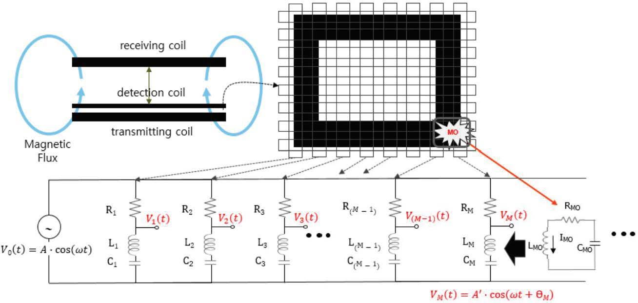
Figure 2 depicts the circuit, which includes the first layer detection coil array. It can be seen that L1 is an equivalent inductor for the N/2 detection coils in the first column, whereas LM is the equivalent inductor for the N/2 detection coils included in the Mth column. To increase the change in voltage induced by the MOs, a capacitor is connected serially to each coil set. The capacitance of the capacitor is selected such that a serial LC resonant circuit is configured for the frequency of the alternating current (AC) power that is supplied to the detection coil array.
The resistor R determines the bandwidth and current of the LC resonant circuit. A low value of resistance generates a narrow bandwidth, which results in a sensitive circuit that requires time for stabilizing. Conversely, a high resistance value widens the bandwidth, which reduces the current and results in a reduced amplitude change of the signal. Consequently, it is difficult to detect the changes caused by foreign metal objects.
As indicated in Figure 2, the voltage of each coil set is measured at the node between the resistor RN and coil set LN to compare the magnitude and phase of the voltage. Initially, we considered the voltage magnitude and phase at node 1 when MO was absent between the transmitting and receiving coils. The frequency and phase of the power source can be calculated as f = ω/(2π) and θ, respectively. We applied Kirchhoff’s voltage law to the first column detection coil set to express it in phasor, and the supply voltage VAC and voltage V1 at node 1 can be obtained as follows:
V A C = A θ = R 1 + j ω L 1 + 1 j ω C 1 I 1 ,
V 1 = j ω L 1 + 1 j ω C 1 I 1 .
The impedance Z for each column and impedance Z1 between the ground and node 1 can be expressed as follows:
Z = R 1 + j ω L 1 + 1 j ω C 1 ,
Z 1 = j ω L 1 + 1 j ω C 1 .
As the frequency of the voltage supplied is the resonant frequency of the series L1 and C1 circuits, the reactance of Z, jωL1 + 1/(jωC1), is zero. Therefore, Z = R1 in Equation (3), V1 = 0 in Equation (2), and Z1 = 0 in Equation (4).
Subsequently, we considered a case where the MO exists on a detection coil. As indicated in Figure 3, the MO is modeled as an RM-LM-CM series circuit, and the MO is placed on the detection coil set L1, where M denotes the mutual inductance between L1 and LM.
When Kirchhoff’s voltage law is applied to the detection coil set with L1 and MO, the voltage V1w at node 1 changes, owing to the mutual inductance between L1 and LMO.
R M + j ω L M + 1 j ω C M I M j ω M I 1 w = 0 ,
Z M = R M + j ω L M + 1 j ω C M , I M = j ω M Z M I 1 w .
V A C = R 1 + j ω L 1 + 1 j ω C 1 I 1 w j ω M I M = R 1 + j ω L 1 + 1 j ω C 1 + ω 2 M 2 Z M I 1 w ,
V 1 w = j ω L 1 + 1 j ω C 1 + ω 2 M 2 Z M I 1 w ,
where V1w and I1w indicate that the voltage generated at node 1 by the MO and the current flowing through the detection coil set are different from those previously observed. Equation (6) verifies that the resistance and reactance components are modified by the presence of the MO. The impedance Zw in the first column is changed by the MO, and the impedance Z1w between the ground and node 1 can be calculated as follows:
Z w = R 1 + j ω L 1 + 1 j ω C 1 + ω 2 M 2 Z M ,
Z 1 w = j ω L 1 + 1 j ω C 1 + ω 2 M 2 Z M ,   ω 2 M 2 Z M = ω 2 M 2 Z M Z M * R M j ω L M 1 ω C M .
Similarly, as jωL1 + 1/(jωC1) = 0, Zw and Z1w can be simplified as
Z w = R 1 + ω 2 M 2 Z M Z M * R M j ω L M 1 ω C M ,
Z 1 w = ω 2 M 2 Z M Z M * R M j ω L M 1 ω C M ,   Z 1 w = ω 2 M 2 Z M Z M * R M 2 + ω L M 1 ω C M 2 .
Figure 4a,b depicts the phasor diagrams of impedance, beginning from the ground, capacitor, inductor, and resistor sequentially, considering the presence and absence of the MO, respectively.
Figure 4a indicates that the impedance Z1 = j(ωL1 − 1/(ωC1) at node 1 is zero in the absence of the MO, owing to ωL1 = 1/(ωC1) and the impedance Z = R1 on the entire bridge. In other words, the phase of the voltage VAC applied to Z, and that of current I1 are identical because only the resistance component exists. Additionally, R1, L1, and C1 exist on one bridge, resulting in identical currents in IR1, IL1, and IC1. At node 1, with an inductor, the voltage is 90° faster than the current. Consequently, the phase of V1 is 90° faster than that of current IL1, and a 90-degree phase difference exists between VAC and V1.
When the MO is inserted, the resistance component increases and the reaction component decreases, as indicated in Equation (9). Therefore, the phase of impedance Z1w is no longer zero, as depicted in Figure 4b. As the impedance Z1w at node 1 has a constant magnitude, owing to the increased resistance and reduced reaction, the magnitude of the voltage is not zero, and the phase of the voltage VAC and current I1w on the bridge differ by the phase θ of Zw. Furthermore, the phase of the voltage at node 1, which is 90° faster than the phase of current I1w, results in a phase difference of 90–θ° between the voltage V1w and the power source voltage VAC. In other words, the voltage signal becomes greater than that observed in the circuit without the MO, and the phase difference with the voltage VAC decreases by the phase θ of the changed impedance.
To detect the MO, we propose multiplying the voltage magnitude at the node by the phase difference and calculating the rate of change, using Equation (11). However, because the phase difference decreases by phase θ of the inserted MO, the rate of change is calculated as 90 − (phase difference) = 90 − (90 − θ) = θ, such that the phase difference has a larger value when MO is inserted.
V × 90 P h a s e d i f f . = V × 90 P h a s e d i f f . n o d e V × 90 P h a s e d i f f . r e f V × 90 P h a s e d i f f . r e f
At this juncture, the reference values are the values measured in the absence of the MO. If a change of more than a certain magnitude is detected compared to the value observed in the absence of the MO, we considered that the MO was inserted.

3. Results

3.1. Implementation

Figure 5 depicts the detection coil set array. This detection coil set array was made on a four layer FR4 PCB with 1 mm thickness. The dimensions of the array and one detection coil are 300 mm × 200 mm and 49 mm × 49 mm, respectively. The number of turns of each detection coil is 30. The wire width is 0.3 mm and the wire spacing is 0.5 mm.
A total of twenty-four (6 × 4) detection coils are used. There are twelve detection coils in the first layer (detection coils marked with “C” suffix in Figure 5, and two coils in the same column, such as C1A and C1B, which are connected to make one set, such as C1. Therefore, there are a total of six coil sets, C1, C2, C3, C4, C5 and C6, in the first layer with inductances of 40 µH. Conversely, the detection coils in the fourth layer are connected between three coils in the same row, such as R1A, R1B and R1C. Therefore, there are a total of four coil sets, R1, R2, R3 and R4, in the second layer with inductances of 60 µH. In the second and third layers, there are return wires of the coil sets in the first and fourth layers, respectively. At 800 kHz resonance, capacitors with capacitances of 1000 pF and 680 pF are connected to the first and second layers of the detection coil set with inductances of 40 µH and 60 µH, respectively.
The transmitting and receiving coils of the wireless power transfer (WPT) system are made by using a 4 mm Litz wire. The core dimensions of these coils is 300 mm × 200 mm, similar to the detection coil array. The turn number of the transmitting coil and the receiving end coil are 20 and 5, respectively, in a ratio of 4:1. The transmitting coil lowers the reactive power by connecting two 10-turn coils in parallel to increase inductance. As shown in Figure 6, the coils are wrapped with 3 mm Teflon and 2 mm ferrite materials are used for magnetic shielding. The detection coil array is placed on the top of the transmitter.
Figure 7 depicts the wireless power transfer system and the proposed MOD system. The 2-kW/85-kHz power transfer system is located on the left side of the figure and a power transmitting coil is placed under the detection coil set array. The capacitors, resistors, and analog-to-digital converters (ADCs) of the proposed MOD system are arranged at the bottom and right, respectively. The 800-kHz AC power is supplied through the AC generator. The experiment was conducted with a distance between the transmitting coil and the receiving coil of 10 cm. The power transmitting coil, the power receiving coil and the detection coil set array were all arranged parallel to each other, and their centers were aligned in the same z-axis direction. Metal objects were placed on the detection coil set array.
To measure the peak value and phase difference of the voltage across the detection coil sets, we developed and implemented a simple digital signal processing circuit using 60-MHz 16-bit ADCs. A sample counter was set to zero each time the AC source signal changed from negative to positive and increased by one at each sampling moment. As the frequency of the supplied AC signal was 800 kHz, 75 samples were measured per period. The phase difference between the samples was 4.8°. When the voltage of each node changed from negative to positive, we checked the sample counter value and calculated the phase difference between the voltage of each node and the AC source signal. To increase the phase resolution, we applied a linear interpolation to the negative and positive values before and after the change in the sign of the signal. The maximum value of the signal was averaged by determining the maximum positive value for each period.

3.2. Experimental Results

Table 1 summarizes the details of the three specimens of metal objects used in the experiment, namely a 500 Korean won coin, a 10 Korean won coin, and a clip. Each specimen was placed on the center of the detection coil C1A of the first layer, and the phase difference of the signal was measured. As depicted in Figure 8, an AC voltage of 800 kHz ± 2.85 V was supplied to the detection coil.
As indicated in Table 2, when no foreign metal object exists between the coils, the peak value of the voltage at node 1 is 0.62 V, and the phase relative to the voltage source is 70.3°. Theoretically, when the LC circuit resonates with the frequency of the power signal, the voltage magnitude at node 1 is 0 V, and the phase relative to the voltage source is 90°. However, the resonance frequency of the selected inductor and capacitor is approximately 795 kHz, and the magnitude of each component lies within the margin of error. Therefore, the implemented circuit does not truly form an LC resonant circuit.
For specimens 1, 2, and 3, the peak values of the voltage are 1.13 V, 0.89 V, and 0.69 V, whereas the phases are 38.4°, 35.8°, and 23.8°, respectively. In the case of specimen 1, the rate of change was approximately 82% when only the peak value of the voltage was calculated considered; conversely, it was approximately 94.9% when calculated using only the phase. However, the rate of change calculated by multiplying the two values was approximately 255%. Moreover, the rate of change was approximately 34% for the clip, which was the smallest specimen. In other words, when detecting foreign metal objects by considering both factors rather than only one factor, the rate of change increases. Hence, we recommend considering both the magnitude and phase of the voltage to detect small foreign metal objects effectively.
In order to compare with the previous papers, additional experiments were conducted on 20 mm × 20 mm and 30 mm × 30 mm aluminum foils, and the results are summarized in Table 3. Table 3 summarizes the variation in the measured values with an MO compared to the measured values without an MO. Overall, an MO with 20–30 mm in diameter changes voltage by 45% or more. However, we consider the phase variation as well as the voltage variation, and the phase variation appears to be as significant as the voltage variation. Therefore, when the voltage and the phase difference are considered together, the detection sensitivity is increased.
In order to investigate the detectability according to the position of an MO, the voltage and phase were measured by placing the MO on the detection coil C1A of the first layer and the detection coil R4A of the second layer as shown in Figure 9. The first represents when the MO is in the center of the C1A, the second when it is placed at the edge of the C1A, and the third represents when it spans C1A and R4A. The fourth represents when it is placed at the edge of the R4A, and the fifth represents when it is placed in the center of the R4A. The sixth and seventh are cases where it is placed at the edge of C1A and R4A, respectively, and the eighth represents where it spans four coils.
As can be seen from Table 4 and Figure 10, when the MO is in the center of the coil, the change of voltage and phase is the largest, and the change becomes smaller as it moves away from the center. When the metal is on the other coil area, there is little difference from the magnitude measured when there is no metal. If a metal is placed across several coils, such as position 3 and 8 in Figure 9, the change of the voltage and phase measured in one coil circuit is relatively small. However, since changes of voltage and phase occur simultaneously in the circuit of the coils on which the MO is placed, the MO can be detected by association.
Since the WPT system and the MOD system are designed to resonate at 85 kHz and 800 kHz, respectively, they are highly unlikely to interfere with each other. However, since the magnitude of the voltage supplied to the two system is more than 600 times, we checked whether the magnetic field generated by the WPT affects the detection coils. As shown in Figure 11a, the output voltage of the power transmitting coil is 1.98 kV/85 kHz through the inverting circuits. At this point, the output voltage of the detection coil is an 800 kHz signal, fluctuating at 85 kHz. That is, the magnetic field generated by the WPT system is detected by the detection coil. Therefore, the 85 kHz interference by the WPT system is removed using an 85 kHz rejection filter. As illustrated in Figure 11b, when an output signal is converted into a frequency band through FFT, an 85 kHz signal larger than 800 kHz is observed, but the 85 kHz signal is removed after filtering.
Conversely, an experiment was conducted to confirm the effect of the MOD system on the WPT system. In Figure 12, the first shows the output voltage of the power transmitting coil and the output voltage of the power receiving circuit when there is no detection coil set array. The second and third show output voltages when a detection coil set array is placed on the transmission coil and power to the MOD system is only supplied in the third case. When a voltage of the same magnitude is supplied to the power transmission circuit for three cases, the output voltage of the power transmitting coil in the first, second and the third case is 1.199 kV, 1.186 kV and 1.186 kV, respectively. Because the power transmitting and receiving coils are tuned again after including the detection coil array in the WPT system, the characteristics of the power transmitting coil inevitably differ when the detection coil is either present or not present. However, in all three, the ratio of the receiving voltage to the transmitting voltage is arounds 0.08, which confirms that there is little effect on the performance of the WPT system.

4. Conclusions

In this study, we propose a system for detecting foreign metal objects in wireless high-power transfer systems, with a certain separation distance between the transmitting and receiving coils. We added detection coil arrays and connected series capacitors to each coil array to construct an LC resonant circuit that can detect the MO. When a foreign metal object is inserted between the transmitting and receiving coils, the impedance of the detection coil changes. However, the impedance change is greater in the LC resonant circuit than that observed in the coil-only circuit. As the impedance changes, both the magnitude and phase of the voltage change. Therefore, we considered the detection of foreign metal objects based on the changes in both components. Additionally, we developed a simple circuit to detect the phase. The proposed method was verified by implementing a wireless power transfer system and detection system. The voltage across the detection coil in the absence of foreign metal object was determined as the reference value. In cases where a change in the magnitude and phase of the voltage occurred over a certain amount compared to the reference value, we concluded that a metal object was inserted. When the magnitude and phase of the voltage were considered for a 500 Korean won coin, the values changed by 82% and 94%, respectively. However, we confirmed that a change of approximately 255% occurs when both components are considered. More specifically, we observed a change of approximately 34% for a clip. This result validated that the proposed method is able to detect even small foreign metal objects efficiently.

Author Contributions

Conceptualization, S.K., W.C. and Y.L.; Formal analysis, S.K.; Investigation, S.K., W.C. and Y.L.; Methodology, S.K. and Y.L.; Project administration, Y.L.; Software, S.K. and W.C.; Supervision, Y.L.; Validation, S.K.; Writing—original draft, S.K.; Writing—review and editing, S.K., W.C. and Y.L. All authors have read and agreed to the published version of the manuscript.

Funding

This work was partly supported by Korea Evaluation Institute of Industrial Technology (KEIT) grant funded by the Korea government (MOTIE) (No.20003574, The development of energy independent smart tag based on Epaper for optimization of production logistics flow and flexible timely manufacturing).

Informed Consent Statement

Not applicable.

Conflicts of Interest

The authors declare no conflict of interest.

References

  1. Machura, P.; De Santis, V.; Li, Q. Driving Range of Electric Vehicles Charged by Wireless Power Transfer. IEEE Trans. Veh. Technol. 2020, 69, 5968–5982. [Google Scholar] [CrossRef]
  2. Ahmad, A.; Alam, M.S.; Chabaan, R. A Comprehensive Review of Wireless Charging Technologies for Electric Vehicles. IEEE Trans. Transp. Electrif. 2018, 4, 38–63. [Google Scholar] [CrossRef]
  3. Patil, D.; McDonough, M.K.; Miller, J.M.; Fahimi, B.; Balsara, P.T. Wireless Power Transfer for Vehicular Applications: Overview and Challenges. IEEE Trans. Transp. Electrif. 2018, 4, 3–37. [Google Scholar] [CrossRef]
  4. How Wireless EV Charging Works for Tesla Model S. Available online: https://www.pluglesspower.com/learn/wireless-ev-charging-works-tesla-model-s/ (accessed on 1 July 2021).
  5. Wireless Power Transfer for Light-Duty Plug-in/Electric Vehicles and Alignment Methodology J2954_202010. Available online: https://www.sae.org/standards/content/j2954_202010/ (accessed on 1 July 2021).
  6. Wireless EV Charging Gets a Boost: Single Standard will Harmonize System up to 11 kW. Available online: https://www.greencarreports.com/news/1130055_wireless-ev-charging-gets-a-boost-single-standard-will-harmonize-systems-up-to-11-kw (accessed on 1 July 2021).
  7. Xia, J.; Yuan, X.; Li, J.; Lu, S.; Cui, X.; Li, S.; Fernández-Ramírez, L.M. Foreign Object Detection for Electric Vehicle Wireless Charging. Electronics 2020, 9, 805. [Google Scholar] [CrossRef]
  8. Zhang, Y.; Yan, Z.; Zhu, J.; Li, S.; Mi, C. A review of foreign object detection (FOD) for inductive power transfer systems. eTransportation 2019, 1, 100002. [Google Scholar] [CrossRef]
  9. Cheng, B.; Lu, J.; Zhang, Y.; Pan, G.; Chabaan, R.; Mi, C.C. A Metal Object Detection System with Multilayer Detection Coil Layouts for Electric Vehicle Wireless Charging. Energies 2020, 13, 2960. [Google Scholar] [CrossRef]
  10. Xiang, L.; Zhu, Z.; Tian, J.; Tian, Y. Foreign Object Detection in a Wireless Power Transfer System Using Symmetrical Coil Sets. IEEE Access 2019, 7, 44622–44631. [Google Scholar] [CrossRef]
  11. Jeong, S.Y.; Kwak, H.G.; Jang, G.C.; Choi, S.Y.; Rim, C.T. Dual-Purpose Nonoverlapping Coil Sets as Metal Object and Vehicle Position Detections for Wireless Stationary EV Chargers. IEEE Trans. Power Electron. 2018, 33, 7387–7397. [Google Scholar] [CrossRef]
  12. Kim, S.; Jung, H.; Ju, Y.; Lim, Y. A Novel Metal Foreign Object Detection for Wireless High-Power Transfer Using a Two-Layer Balanced Coil Array with a Serial-Resonance Maxwell Bridge. Electronics 2020, 9, 2070. [Google Scholar] [CrossRef]
  13. Jeong, S.Y.; Thai, V.X.; Park, J.H.; Rim, C.T. Self-Inductance-Based Metal Object Detection with Mistuned Resonant Circuits and Nullifying Induced Voltage for Wireless EV Chargers. IEEE Trans. Power Electron. 2019, 34, 748–758. [Google Scholar] [CrossRef]
Figure 1. Proposed detection coil array. (a) Layout table for the detection coils. (b) The first layer detection coil array. (c) The second layer detection coil array.
Electronics 10 02952 g001
Figure 2. Equivalent metal object detection circuit.
Electronics 10 02952 g002
Figure 3. Equivalent metal object detection circuit when a metallic object (MO) is inserted between the transmitting and receiving coils.
Electronics 10 02952 g003
Figure 4. Phasor diagram of the impedance. (a) in the absence of a metallic object (MO). (b) in the presence of the MO.
Electronics 10 02952 g004
Figure 5. The detection coil set array.
Electronics 10 02952 g005
Figure 6. Side view of the wireless power transfer coils.
Electronics 10 02952 g006
Figure 7. The wireless power transfer system and the proposed MOD system.
Electronics 10 02952 g007
Figure 8. Measured voltage signals.
Electronics 10 02952 g008
Figure 9. MO positions in a detection coil array.
Electronics 10 02952 g009
Figure 10. Voltage and phase variation according to MO’s position.
Electronics 10 02952 g010
Figure 11. Removal of interference signal from the detection coil by the WPT system. (a) Input voltage of the inverting circuits and output voltage of the power transmitting coil and (b) output voltage of the detection coil before and after signal removal of the WPT system.
Electronics 10 02952 g011
Figure 12. The output voltage of the power transmitting and receiving coil. (a) without a detection coil array, (b) with a detection coil array, and (c) with a detection coil array to which power is supplied.
Electronics 10 02952 g012
Table 1. Specimens of metal objects used in the experiment.
Specimen 1Specimen 2Specimen 3
500 Korean won coin10 Korean won coinclip
Electronics 10 02952 i001
diameter 2.65 cm
Electronics 10 02952 i002
diameter 1.8 cm
Electronics 10 02952 i003
3.5 cm × 0.8 cm
Table 2. Circuit characteristics with the presence and absence of metal object specimens in the experiment.
No MOSpecimen 1Specimen 2Specimen 3
Max(|V|)0.621.130.890.69
Max(|V|) variation rate-82.2643.5411.29
Phase difference(°)70.351.654.266.2
Modified_Phase(°)19.738.435.823.8
Modified_Phase variation rate-94.92381.7220.8
Max(|V|) × (Modified_Phase)12.21343.3931.86216.42
Max(|V|) × (Phase) variation rate-255160.9334.479
Table 3. Comparison of voltage and phase variation with previous papers.
Metal TypesItemThis Paper[13][9]
500 KRW
(75% copper, 25% nickel, 26.5 mm in diameter)
voltage82.2%45.5%-
phase94.9%--
US One-cent coin
(97.5% zinc, 2.5% copper, 19.05 mm in diameter)
voltage--48.7%
Aluminum foil
20mm × 20mm
voltage51.6%68.2%-
phase87.8%--
Aluminum foil
30mm × 30mm
voltage101.6%77.2%-
phase115.7%--
Table 4. Voltage and phase variation according to positions.
Place1(C1A)2(C1A)3(C1A)3(R4A)4(R4A)5(R4A)6(C1A)7(R4A)8(C1A)8(R4A)
Max(|V|)1.130.810.640.600.811.030.740.690.630.59
Modified_Phase(°)38.437.631.7217.9625.1828.7735.7327.7125.214.0
Max(|V|) × (Phase) variation rate25514566782343851161854335
Publisher’s Note: MDPI stays neutral with regard to jurisdictional claims in published maps and institutional affiliations.

