Article

Dual-Polarized Stacked Patch Antenna for Wireless Communication Application and Microwave Power Transfer

College of Electronic and Information Engineering, Sichuan University, Chengdu 610064, China
*
Author to whom correspondence should be addressed.
Electronics 2021, 10(23), 2988; https://doi.org/10.3390/electronics10232988
Submission received: 20 October 2021 / Revised: 18 November 2021 / Accepted: 25 November 2021 / Published: 1 December 2021
(This article belongs to the Special Issue Novel Microwave/Millimeter-Wave Devices and Antennas)

Abstract

:
In this paper, a dual-polarized stacked patch antenna for wireless communication and microwave power transfer is proposed. The stacked antenna consists of four rectangular apertures that are etched on the ground plane and four identical cross-placed coupling strips that are set on the upper layer of the ground plane, which are used to excite the top-layer patches. The presented stacked patch antenna was designed as a completely symmetric structure except for the feeding network, resulting in a simple structure and the same radiation patterns for the two polarized ports. The proposed antenna operates at around 5.8 GHz, and the simulation and measured results show that it has a gain of 8.5 dBi and an isolation of 25 dB. The measured antenna efficiency of the two polarized ports at 5.85 GHz was 89.2% and 88.6%, respectively. Finally, a rectifying circuit was designed, and the maximum measured conversion efficiency of the two polarized rectenna was 63.5% and 62.7%, respectively.

1. Introduction

In wireless power transfer (WPT), which is known as contactless power transferring, the electrical energy from a source is transferred to a load without any direct electrical contact. In the early 1960s, W. C. Brown proposed the concept of microwave wireless power transfer (MWPT) for the first time, i.e., transmitting the high-power electromagnetic energy in free space by using a microwave [1]. In the research on the MWPT, the most important thing is to ensure the efficient transmission of electromagnetic energy. The MWPT system is mainly composed of a high-power microwave source, transmitting antenna, receiving antenna, and rectifier circuit. The energy transfer efficiency of MWPT is determined by the conversion efficiency of the microwave source, the radiation efficiency of the transmitting and receiving antenna, and the conversion efficiency of the rectifier circuit.
In this paper, a dual-polarized stacked patch antenna is proposed. A stacked patch antenna is a kind of wideband high gain that has been widely studied and applied for wireless communications [2,3,4,5,6,7,8,9,10,11,12,13,14,15]. In [2], a wideband array with inverted feeding structures was studied. In [3], a wideband dual-polarized patch array was proposed, in which the authors used a novel method to improve the port isolation by setting two vertical metallic sidewalls on the long edges of the ground and employing a modified feeding structure, resulting in a low coupling value of 36.4 dBi between the two input ports. In [4], a wideband slot-coupled stacked antenna was presented with an operating frequency band that covers the UMTS (1920–2170 MHz), WLAN (2.4–2.484 GHz), and UMTS (2500–2690 MHz), which has a wide bandwidth, but the whole antenna has eleven layers in total, and its profile is high. In [5], a wideband array for wireless communication systems was proposed, wherein the proposed array was fed by using a sequential rotation technique, and each patch element was excited by a square ring slot, and the gain and beam width can be changed by adjusting the antenna size. In [6], a massive MIMO antenna using a stacked antenna technique was proposed with an MIMO array operating at 3.7 GHz, with a novel array configuration consisting of 18 subarrays. Each subarray is made by four elements, and a wideband and low profile was achieved. In [7], a high isolation dual-polarized antenna was presented. The antenna consists of two E-shaped patches which are arranged orthogonally. Furthermore, it was fed by two separate probes, which realize a port isolation larger than 30 dB. In [8], a wideband, dual-polarized and high-isolation antenna was proposed. The antenna exhibited a high matching level and obtained broadband and high-isolation properties. In [9], a wideband stacked patch antenna with differentially fed and tuned slot excitations was proposed. In [10], wideband and dual-polarized slot-coupled antenna was studied by using two orthogonal U-shaped feed lines to excite the cross slot, and by adjusting the width and stacked patches, the wideband and high-isolation properties were obtained. In [11], a dual-polarized and low-cost array was proposed. The antenna realized one polarization by using slot-coupled feed, and the other polarization was achieved by feeding it with slotted ground. In [12], a dual-polarized array operating at 4.5 to 5.8 GHz was proposed. The ultra-high, inter-port isolation was obtained by using self-interference suppression structure.
Through the study of the above academic achievements, we designed a novel dual-polarized stacked patch antenna operating at around 5.8 GHz, which is suitable for wireless communication and microwave power transfer. Stacked patch structure and orthogonally feed were applied to achieve wideband impedance matching and high isolation. The proposed antenna has a small size of 60 mm × 60 mm, with an average gain of 8.5 dBi, which is suitable for wireless communication and far-field wireless power transfer.

2. Antenna Design

2.1. Single Polarized Antenna Design

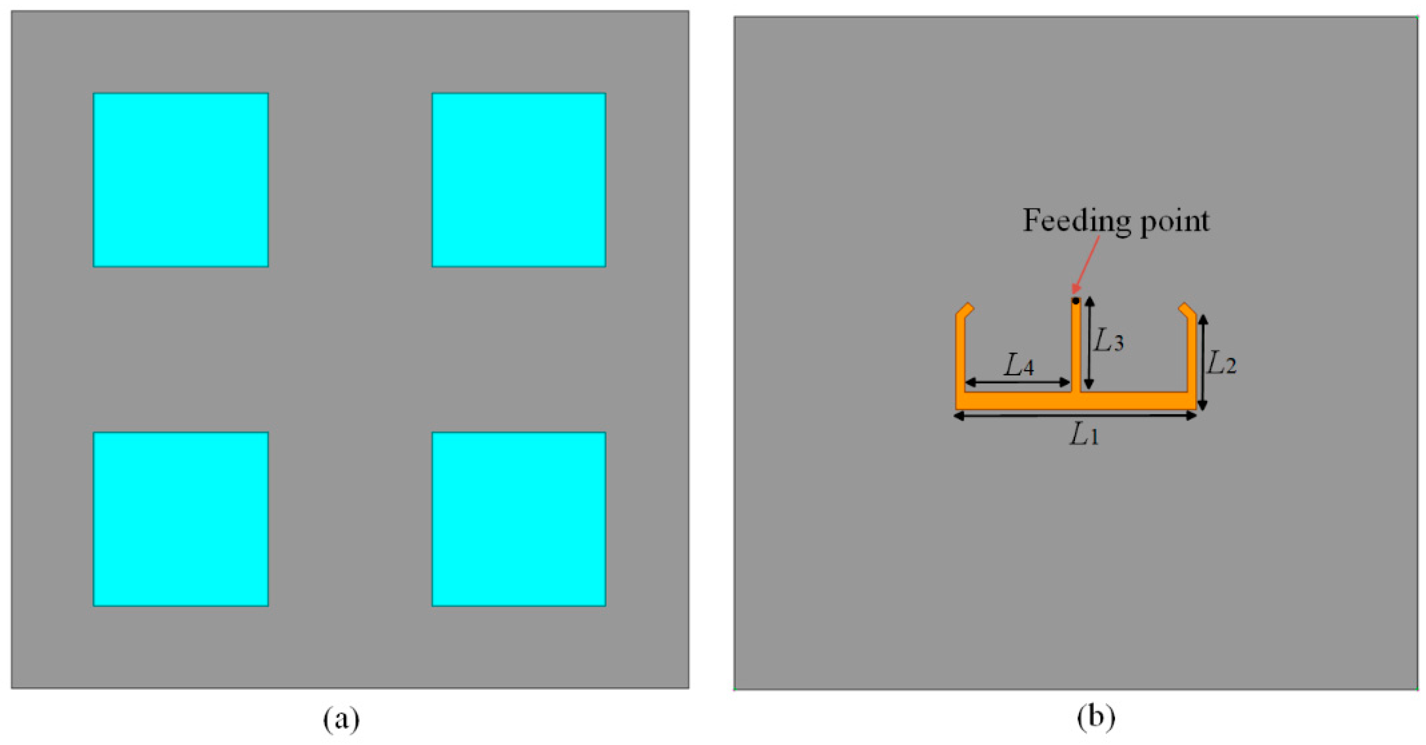
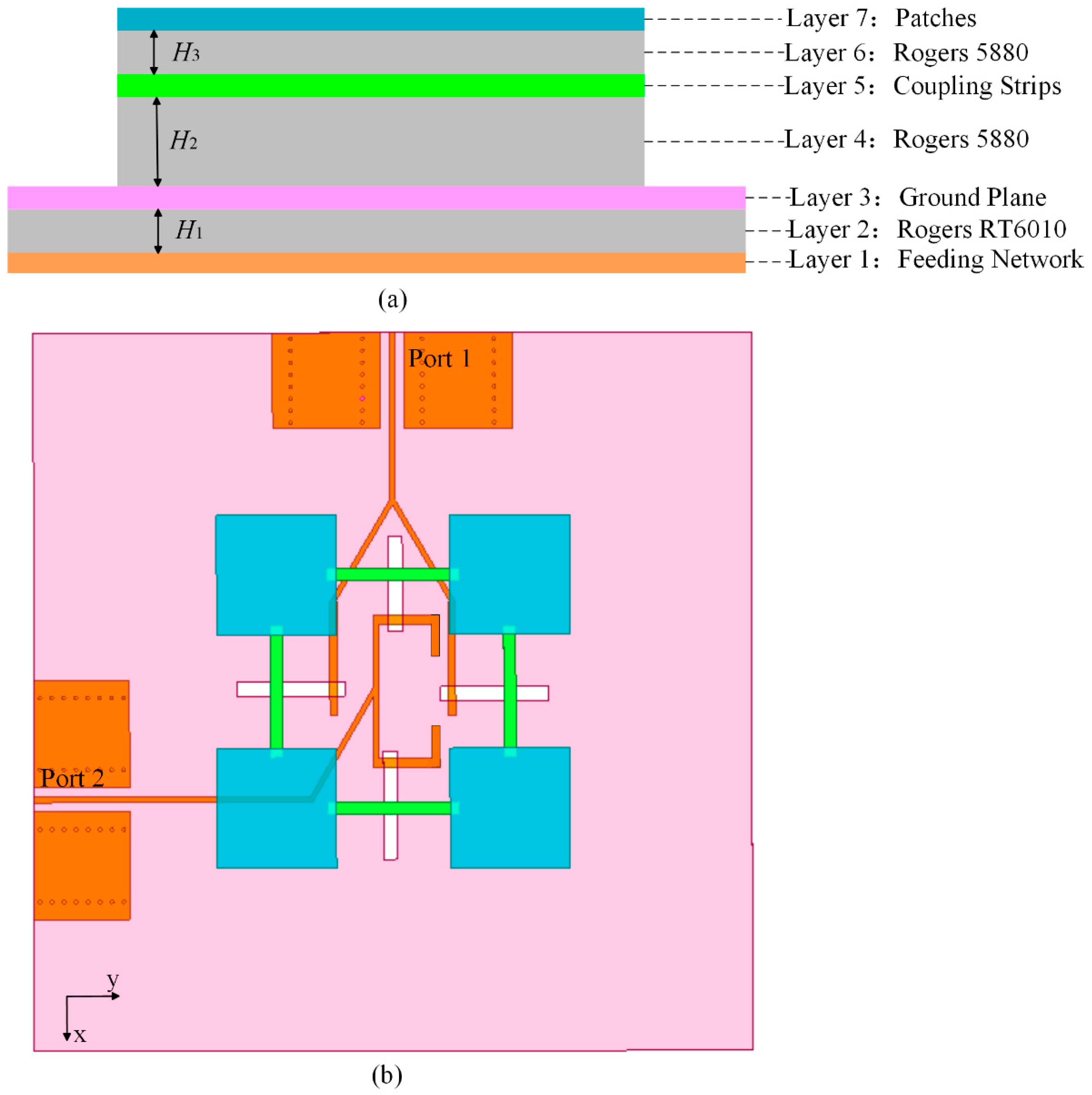
The presented antenna with seven stacked layers is shown in Figure 1 and Figure 2. Layers 1, 3, 5, and 7 are metal layers, and layers 2, 4, and 6 are dielectric substrate layers. Layer 1 is the feed network layer, and an E-shaped feed structure was used; two branches of the E-shaped structure divide the energy to two paths to motivate the top two rectangular slots, generating a single polarization excitation. Layer 3 is the ground plane layer, with a measurement of 60 mm × 60 mm, and four rectangular slots are etched in order to transfer the energy to the top coupling strips. The four rectangular slots are arranged symmetrically on the ground plane. Layer 5 is the coupling strips layer, and the four coupling strips are arranged symmetrically between the dielectric Layer 4 and dielectric Layer 6. Each coupling strip is orthogonal to its bottom rectangular slots. Layer 7 is the radiation patch layer, in which four patches are arranged symmetrically. The power coming from the E-shaped structure is divided into two equal signals, which are coupled to the rectangular slots on the ground plane and then coupled to the top two coupling strips. Finally, the adjacent radiation patches are motivated by the coupling strips.
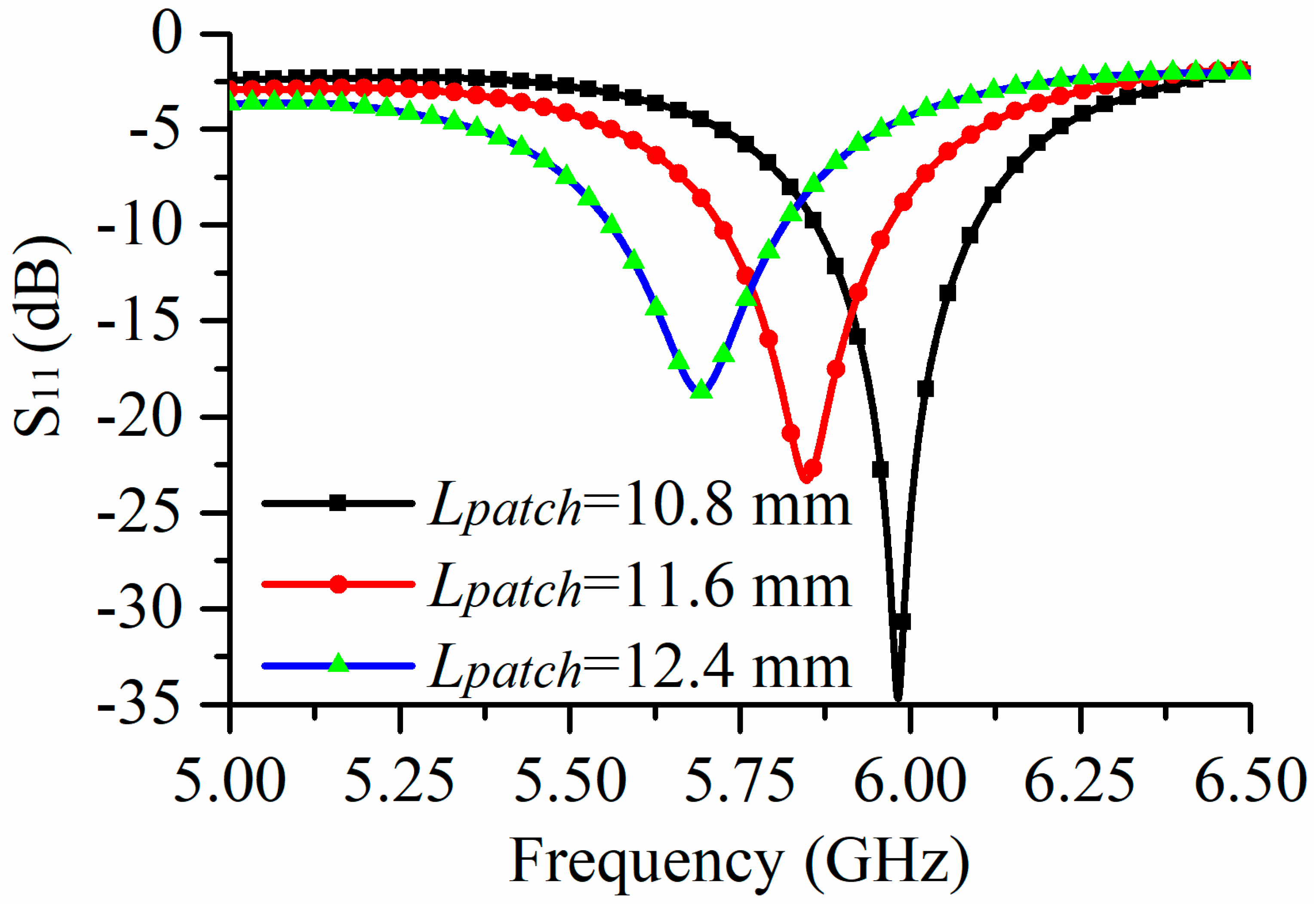
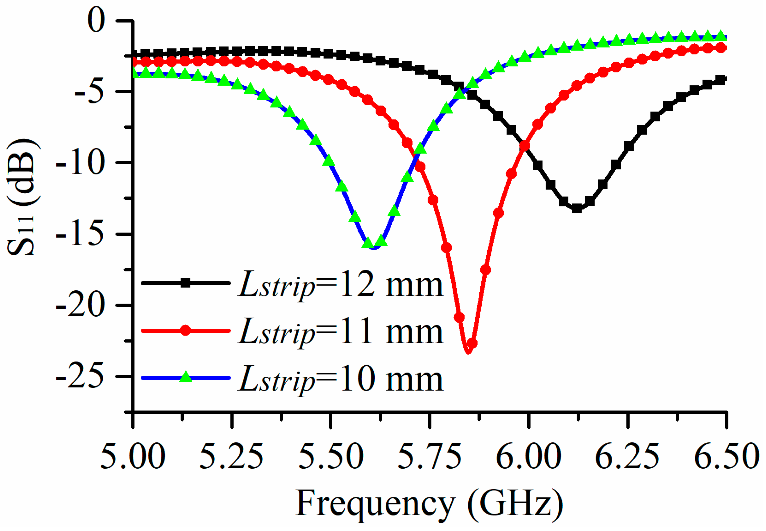
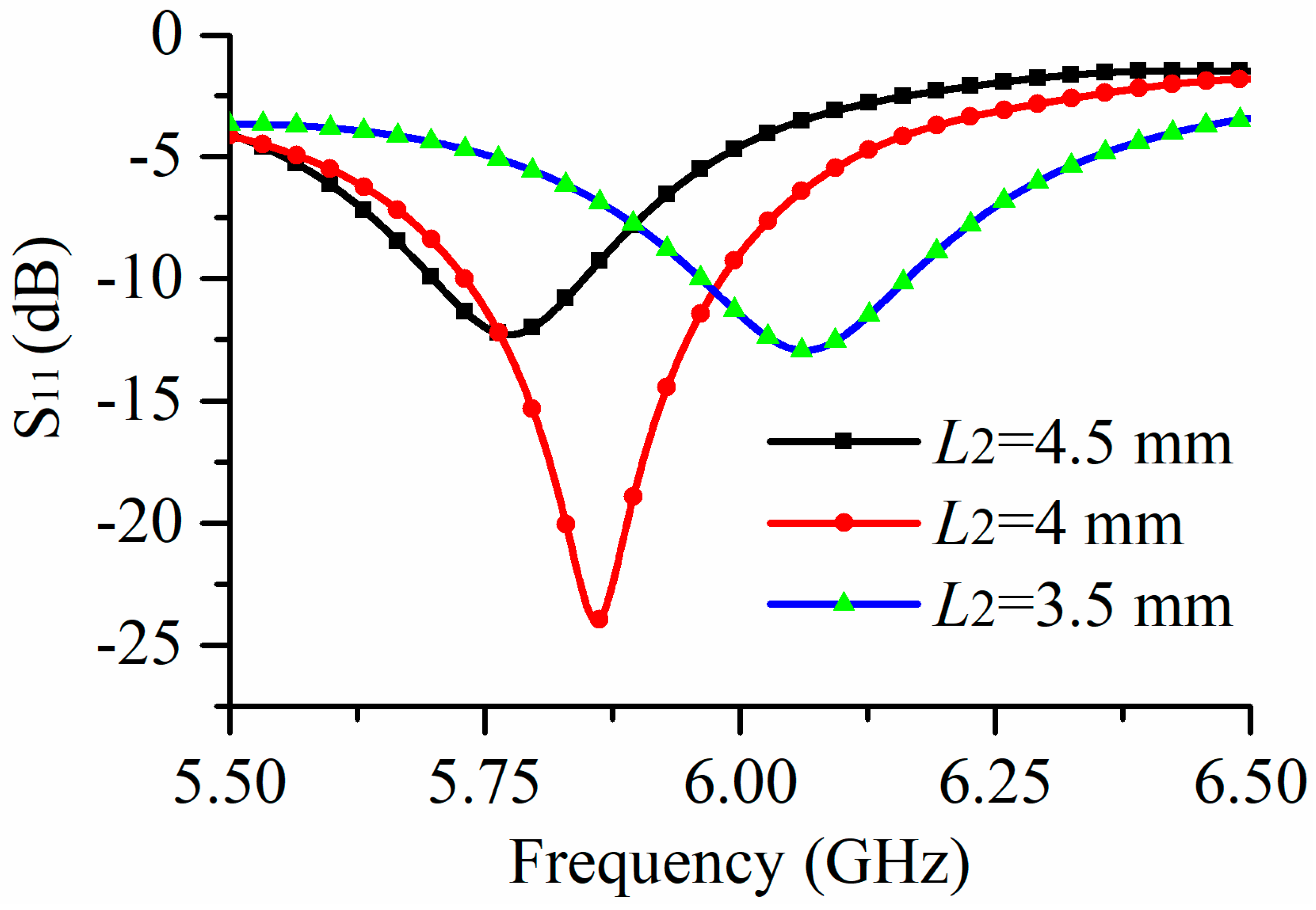
The dielectric substrate material of Layer 2 is Rogers RT6010 (εr = 9.6), and the dielectric substrate material of Layers 4 and 6 is Rogers 5880 (εr = 2.2). The thickness of Layers 2, 4, and 6 is H1 = 0.635 mm, H2 = 1.524 mm, H2 = 0.762 mm, respectively. There are several structure parameters that can affect the antenna performance. The proposed antenna was simulated by using the electromagnetic simulation tool CST Studio Suite software and fed by using a discrete port. Figure 3 shows the simulated S11 when tuning parameter Lpatch. It can be seen that the width of the radiation patch affects the resonance frequency depth. The center resonance frequency moved from 5.98 GHz to 5.68 GHz when tuning Lpatch from 10.8 mm to 12.4 mm with a step increment of 0.8 mm. Figure 4 exhibits the simulated S11 when tuning parameter Lstrip. It is obvious that the center resonance frequency moved from 5.62 GHz to 6.12 GHz when tuning Lstrip from 10.8 mm to 12.4 mm with an increment of 0.8 mm. Figure 5 shows the simulated S11 of the proposed antenna with tuning parameter L2. Note that when L2 increased from 3.5 mm to 4.5 mm, the center resonance frequency moved from 5.75 GHz to 6.06 GHz. The final parameters of the proposed antenna are listed as follows: H1 = 0.635 mm, H2 = 1.524 mm, H3 = 0.762 mm, Lpatch = 11.6 mm, Lslot = 10 mm, Wslot = 1.2 mm, Lstrip = 11 mm, Wstrip = 1 mm, d = 9.5 mm, s = 4.75 mm, L1 = 13.75 mm, L2 = 4 mm, L3= 5.5 mm, L4 = 6.15 mm.

2.2. Dual-Polarized Antenna Design

Due to the symmetric structure, it is easy to achieve dual polarization by arranging another polarized port. As shown in Figure 6, the total layers and substrate materials are the same as the single polarized antenna introduced in Section 2.1. As seen in Figure 6b, the feeding network was reoptimized to achieve dual-polarized properties. For Port 1, a Y-shaped microstrip feed line was used, and its two branches transferred power to the two coupling strips via rectangular slots, resulting in one polarization. For Port 2, a C-shaped microstrip feed line was used, and its two branches transferred power to the two coupling strips via rectangular slots, resulting in another polarization. To facilitate the use of an SMA connector, two short circuits to ground patches were set along to the corresponding feed lines. The total size of the antenna is 60 mm × 60 mm. The total thickness of the antenna is 2.94 mm, which is about 0.056 λ0, where λ0 is the free space wavelength at 5.8 GHz. In Figure 7, the final parameters of the proposed Y-shaped and C-shaped feed line are listed as follows: L1 = 14 mm, L2 = 9.8 mm, L3= 9.5 mm, L4 = 6.15 mm, L5 = 6.15 mm, L6 = 6.15 mm, a = 9 mm, b = 8 mm.
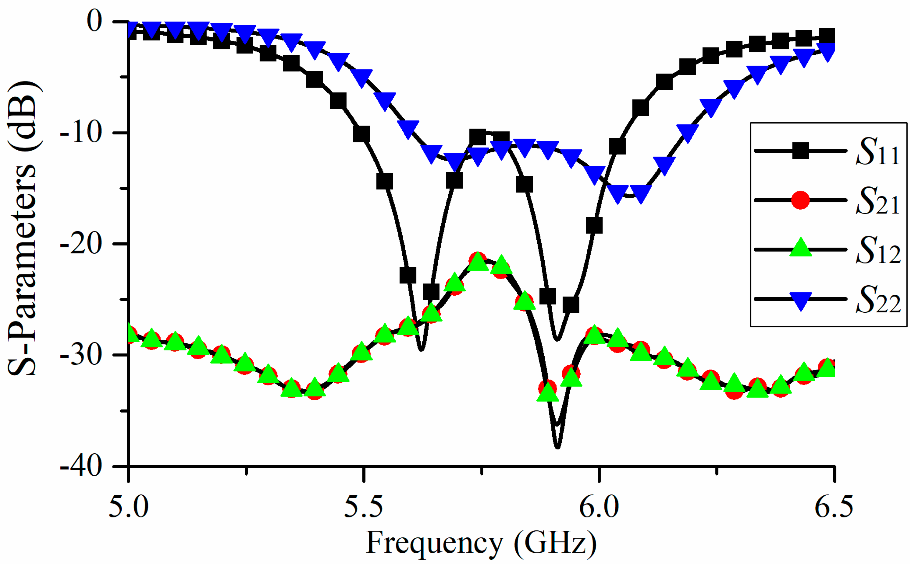
Figure 7 shows the simulation structure of the proposed antenna. Figure 8 shows the S-parameters of the proposed dual-polarized antenna. As can be seen, the common |S11| < −10 dB bandwidth of the two ports was 8.6% at 5.6 GHz–6.1 GHz, which covers the 5.8 GHz frequency band for wireless power transfer. The minimum isolation between the two ports is 22 dB.
Figure 9 exhibits the simulation currents of the proposed dual-polarized antenna at 5.8 GHz. It is obvious that Port 1 generates stable and in-phase currents along the y-axis on the top four radiation patches. However, Port 2 generates another stable and in-phase currents along the x-axis on the top four radiation patches. Dual polarization (horizontal and vertical) was achieved by Port 1 was excited and Port 2 was excited, respectively.

3. Simulated and Measured Results

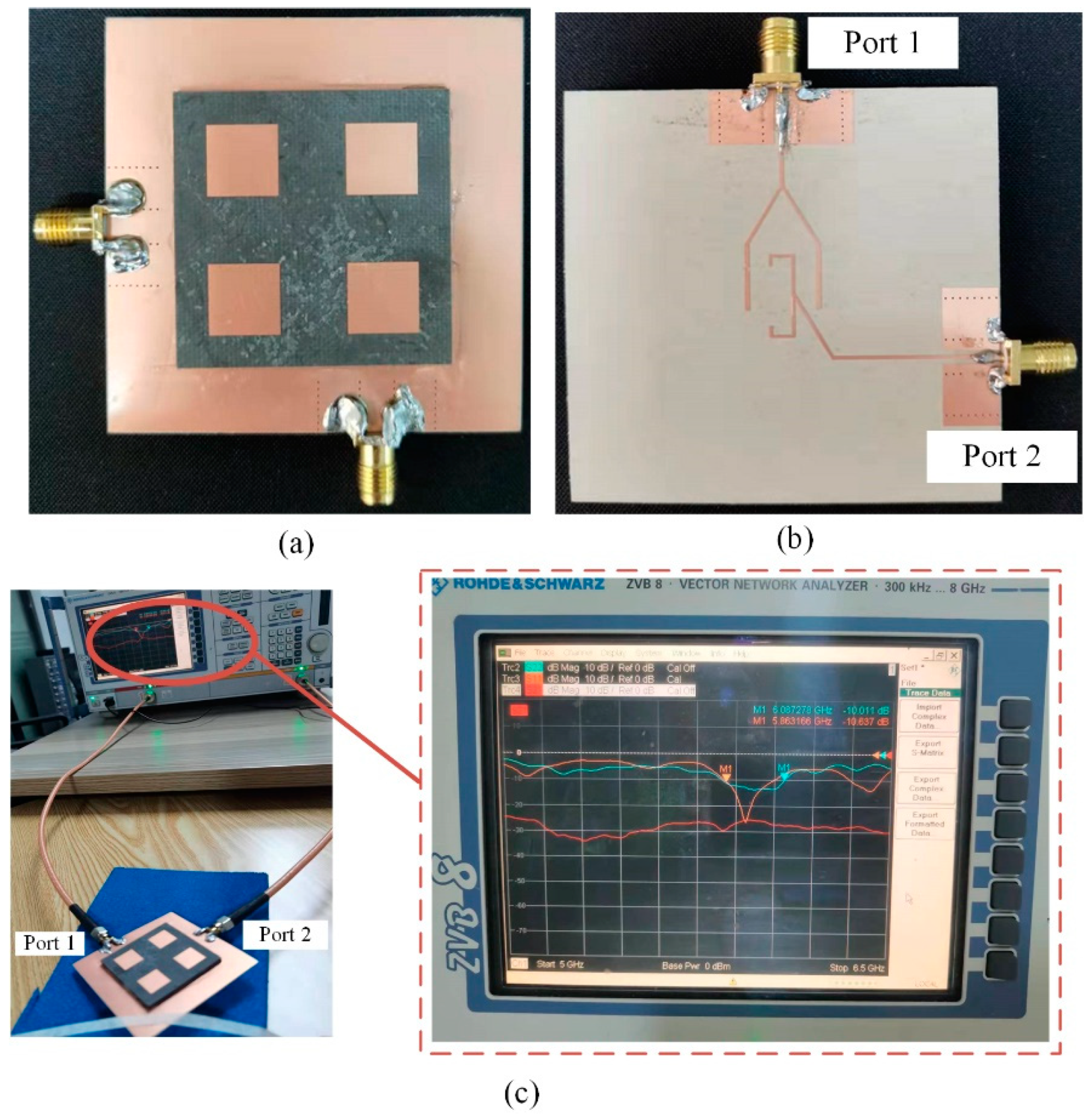
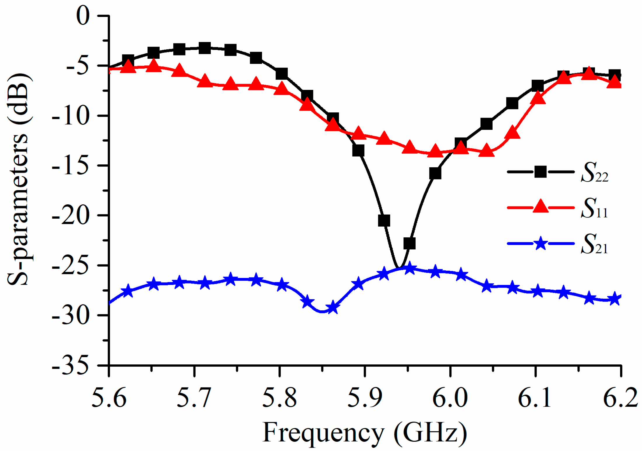
The proposed dual-polarized stacked patch antenna was fabricated by using multilayer PCB structures. The fabrication antenna and measured setup are shown in Figure 10. The two ports of the antenna are connected with SMA connectors. The S-parameters were measured in a laboratory with open space. Figure 11 shows the measured S-parameters of the proposed antenna. One can see that the common measured |S11| < −10 dB bandwidth of the two ports was reached at 5.84 GHz–6.04 GHz. The minimum isolation between the two ports is 25.2 dB. The measured results slightly deviate from the simulation ones due to the issues caused by the manufacturing process and other unexpected influences in the indoor testing environment.
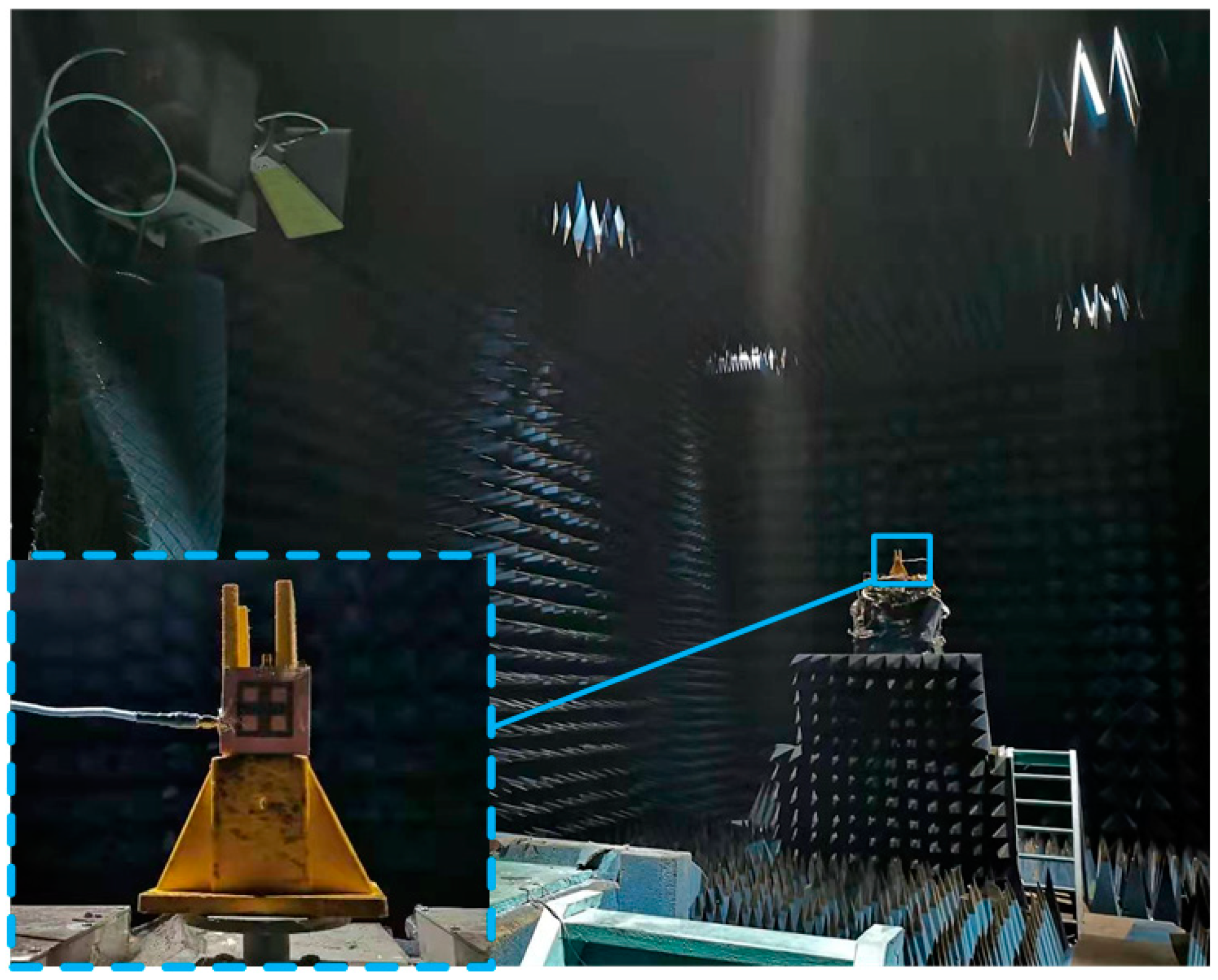
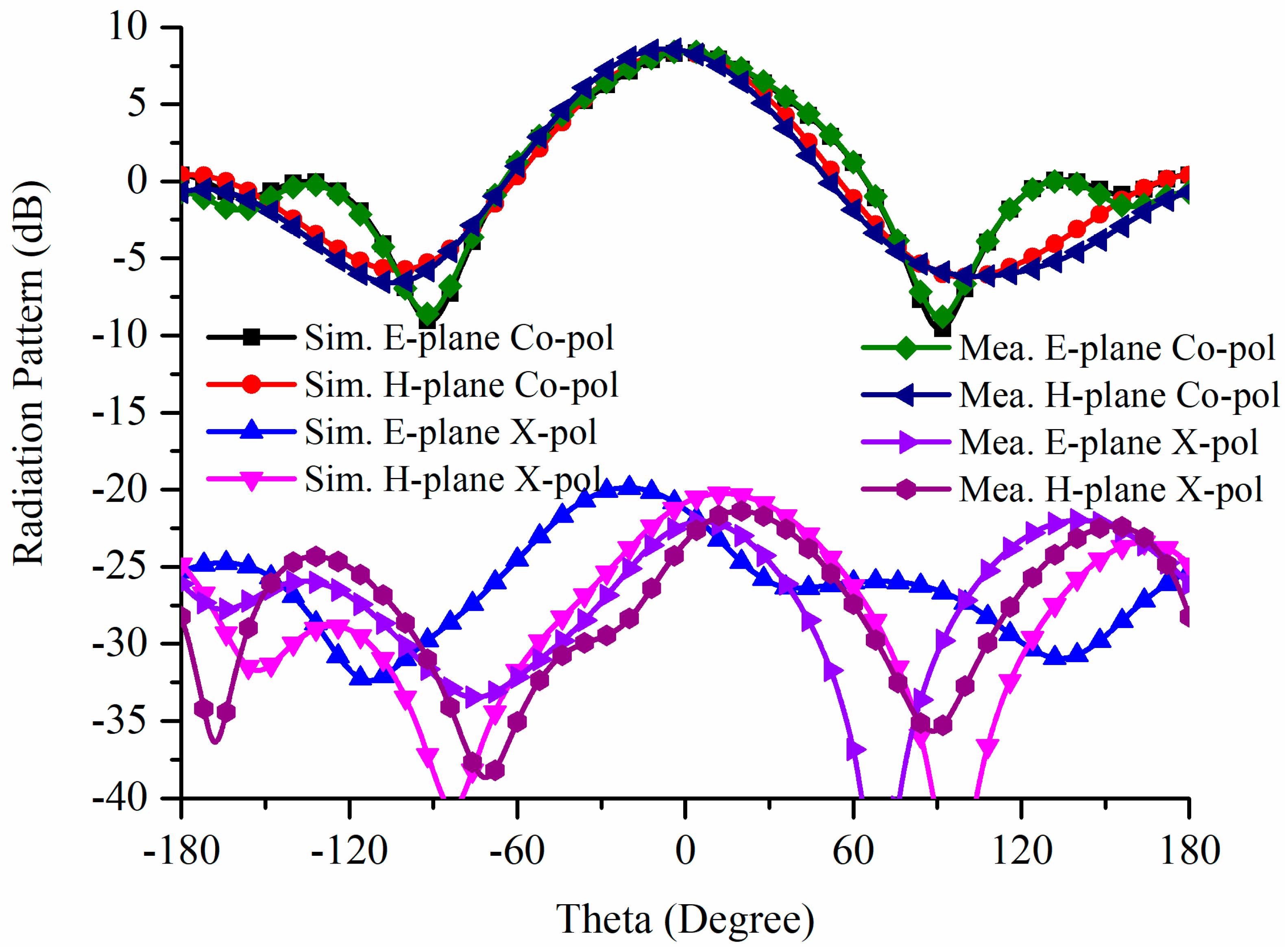
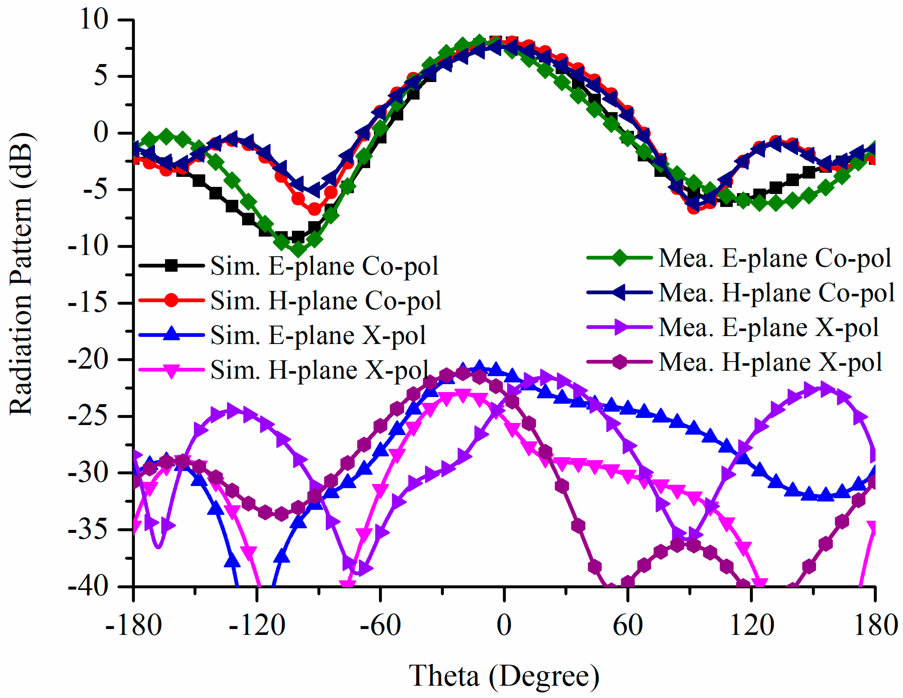
Figure 12 shows the far-field test setup of the proposed antenna. Figure 13 and Figure 14 exhibit the simulated and measured radiation patterns at 5.85 GHz. The simulation results agree well with the measured ones. For Port 1, the measured 3 dB beamwidths of E-plane and H-plane were near 71° and 63°, respectively. For Port 2, the measured 3 dB beamwidths of E-plane and H-plane were near 72° and 65°, respectively. The cross-polarization of the two ports at the boresight was greater than 20 dB. The measured gains of the two polarizations were about 8.5 dBi. For Port 1, the simulated and measured antenna efficiency at 5.85 GHz was 92.1% and 89.2%, respectively. For Port 2, the simulated and measured antenna efficiency at 5.85 GHz was 91.6% and 88.6%, respectively. The decrease of the measured antenna efficiency may have resulted from the loss of cables and manufacturing tolerance.

4. Rectifying Circuit Design

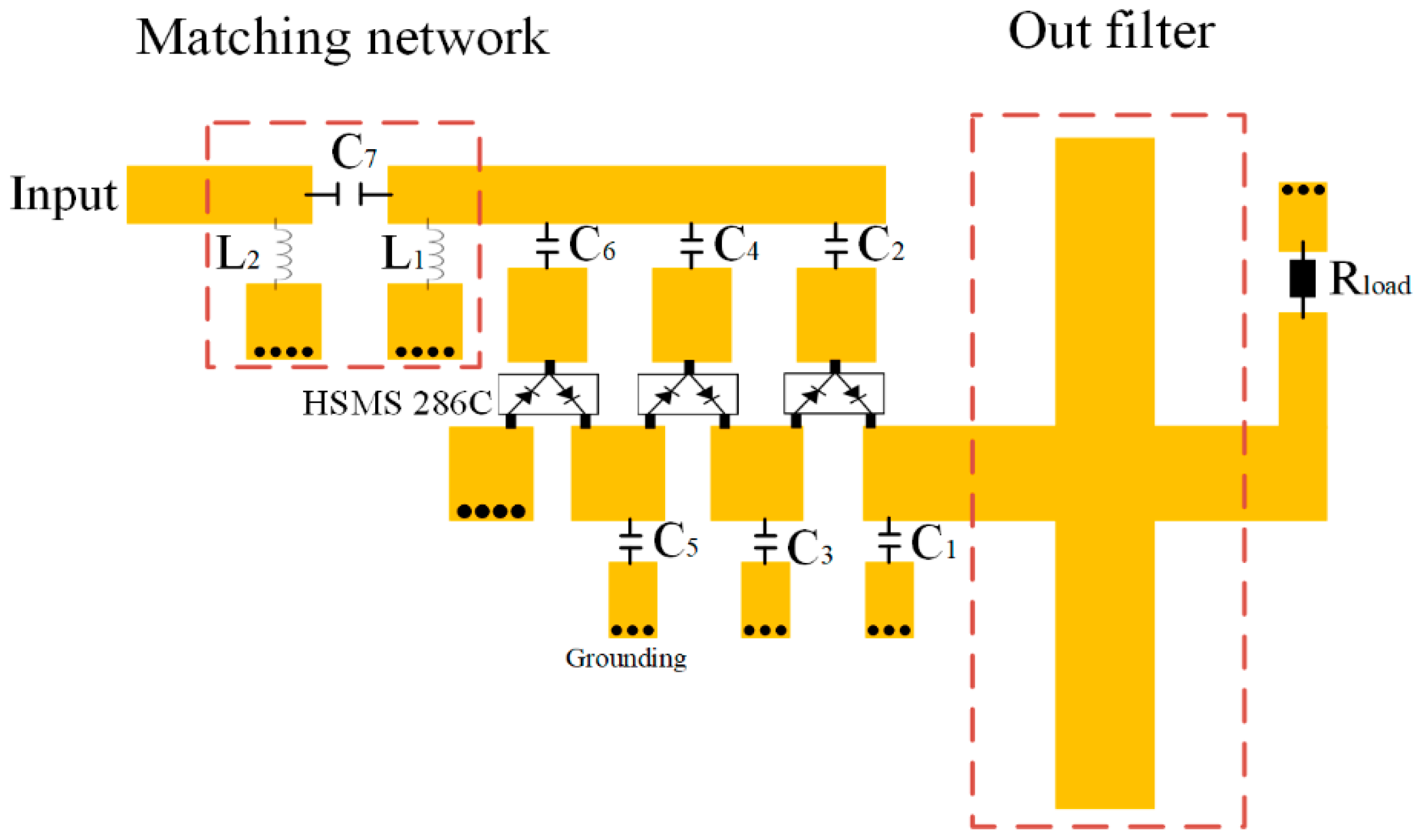
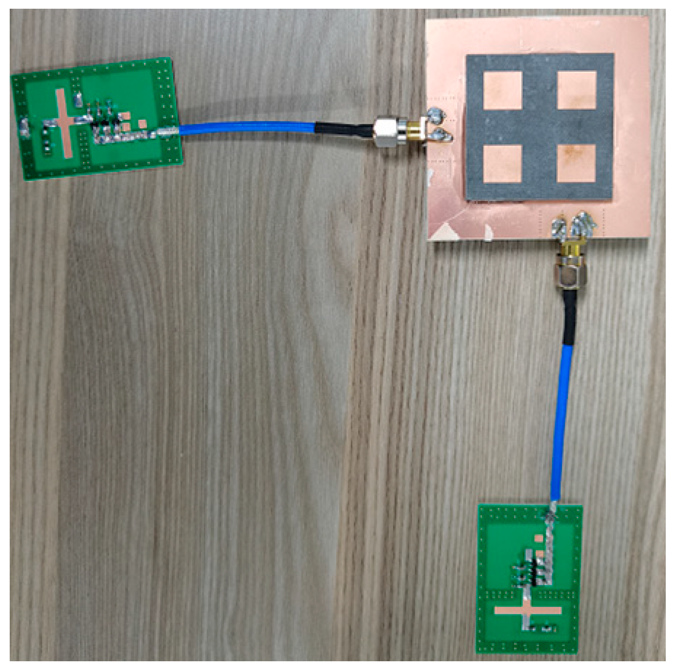
To validate the actual radiation property of the proposed dual-polarized stacked patch antenna, a pair of identical rectifying circuits were designed to perform the microwave power transfer experiment. Figure 15 shows the configuration of the proposed rectifying circuit, printed on a grounded R04350B substrate with a thickness of 1 mm and dielectric constant of 3.48. Three HSMS 286C series Schottky diodes were placed parallel to each other to construct a six-stage rectifier. A Π-typed matching network (L1, L2, C7) was used to adjust the input impedance, and the six pre-capacitors (C1~C6) did not only suppress the high-order harmonics but also blocked the reverse direct currents. At the end of the rectifying circuit, an output filter was applied to suppress the high-order harmonics. The final parameters of the rectifying circuit are listed as follows: C1 = 50 pF, C2 = 50 pF, C3 = 50 pF, C4 = 100 pF, C5 = 100 pF, C6 = 100 pF, C7 = 50 pF, L1 = nH, L2 = nH, Rload = 1000 Ω. Figure 16 shows the fabricated rectifying circuit.
The conversion efficiency, η, can be expressed by
η = V2/(Pin × RL)
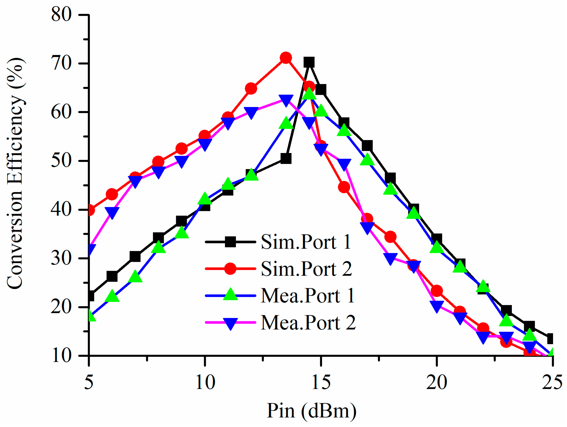
where RL is the load resistance, V is the output DC voltage of the load resistance, and Pin is the input power of the rectifying circuit. The simulation was carried out using electromagnetic simulation tool ADS software. As can be seen from Figure 17, for Port 1, when the input power Pin was 14.2 dBi, the maximum simulated conversion efficiency was 70.2% at 5.85 GHz; for Port 2, when the input power Pin was 13.5 dBi, the maximum simulated conversion efficiency was 71.1%. The rectifying circuit was fabricated as shown in Figure 16, and a pair of rectifying circuits were connected to the two ports of the proposed dual-polarized antenna, acting as a dual-polarized rectenna system. In the test, a 10 dBi standard gain horn antenna was used for transmitting power. The distance between the horn and the rectenna is 1 m. The load resistance RL was set to be 500 Ω, and a multimeter was used to test the output DC voltage. The measured rectenna efficiencies are also shown in Figure 17. It can be seen that, for Port 1, when the input power Pin was 14.2 dBi, the maximum measured conversion efficiency was 63.5% at 5.85 GHz; for Port 2, when the input power Pin was 13.5 dBi, the maximum measured conversion efficiency was 62.7%. The measured efficiencies were lower than the simulated ones. The discrepancy between the simulated and measured results may be caused by: (a) the actual loss of the cables, connectors, and circuit manufacturing; or (b) the real working environment of the components such as HSMS 286C diodes is different from the ideal simulation environment.

5. Conclusions

A dual-polarized high-gain stacked patch antenna for wireless power transfer was proposed. The stacked antenna consists of four rectangular apertures which are etched on the ground plane and four identical cross-placed coupling strips that are set on the upper layer of the ground plane, which are used to excite the top-layer patches. Each rectangular aperture transfers the input power to the corresponding coupling strip above it, and then each coupling strip excites the two adjacent patches simultaneously. The presented stacked patch antenna was designed as a completely symmetric structure except for the feeding network, resulting in a simple structure and low profile. The simulation results of the proposed antenna, operating at around 5.8 GHz, show that it has an average gain of 8.5 dBi and an isolation of 25.2 dB. The measured antenna efficiency of the two polarized ports at 5.85 GHz was 89.2% and 88.6%, respectively. Finally, the maximum measured conversion efficiency of the two polarized rectenna was 63.5% and 62.7%, respectively.

Author Contributions

Conceptualization, L.L. and X.C.; writing—original draft preparation, L.L., Z.L. and Y.T.; writing—review and editing, X.C. All authors have read and agreed to the published version of the manuscript.

Funding

This research was funded by the National Natural Science Foundation of China (U19A2054).

Institutional Review Board Statement

Not applicable.

Informed Consent Statement

Not applicable.

Data Availability Statement

Not applicable.

Conflicts of Interest

The authors declare no conflict of interest.

References

  1. Brown, W.C. The history of wireless power transmission. Sol. Energy 1996, 56, 3–21. [Google Scholar] [CrossRef]
  2. Yun, W.; Yoon, Y.J. A wideband aperture coupled microwave array antenna using inverted feeding structures. IEEE Trans. Antennas Propag. 2005, 53, 861–862. [Google Scholar]
  3. Lau, K.L.; Luk, K.M. A wideband dual-polarized L-probe stacked patch antenna array. IEEE Antennas Wirel. Propag. Lett. 2007, 6, 529–532. [Google Scholar]
  4. Serra, A.A.; Nepa, P.; Manara, G.; Tribellini, G.; Cioci, S. A wide-band dual-polarized stacked patch antenna. IEEE Antennas Wirel. Propag. Lett. 2007, 6, 141–143. [Google Scholar] [CrossRef]
  5. Caso, R.; Serra, A.A.; Pino, M.R.; Nepa, P.; Manara, G. A wideband slot-coupled stacked patch array for wireless communications. IEEE Antennas Wirel. Propag. Lett. 2010, 9, 986–989. [Google Scholar]
  6. Gao, Y.; Ma, R.B.; Wang, Y.P.; Zhang, Q.Y.; Parini, C. Stacked patch antenna with dual-polarization and low mutual coupling for massive MIMO. IEEE Trans. Antennas Propag. 2016, 64, 4544–4549. [Google Scholar] [CrossRef]
  7. Guo, Y.S.; Yang, S.W.; Zhu, Q.J.; Nie, Z.P. A compact dual-polarized double E-shaped patch antenna with high isolation. IEEE Trans. Antennas Propag. 2013, 61, 4349–4353. [Google Scholar]
  8. Barba, M. A high-isolation, wideband and dual-linear polarization patch antenna. IEEE Trans. Antennas Propag. 2008, 56, 1472–1476. [Google Scholar] [CrossRef] [Green Version]
  9. Tang, Z.Y.; Liu, J.H.; Cai, Y.M.; Wang, J.H.; Yin, Y.Z. A wideband differentially fed dual-polarized stacked patch antenna with tuned slot excitations. IEEE Trans. Antennas Propag. 2018, 66, 2055–2060. [Google Scholar] [CrossRef]
  10. Xie, G.J.; Zhang, F.S.; Liu, S.B.; Zhao, Y. A wideband dual-polarized aperture-coupled antenna with embedded in a small metal cavity. IEEE Trans. Antennas Propag. 2020, 68, 7646–7651. [Google Scholar] [CrossRef]
  11. Gao, S.; Sambell, A. Low-cost dual-polarized printed array with broad bandwidth. IEEE Trans. Antennas Propag. 2004, 52, 3394–3397. [Google Scholar] [CrossRef]
  12. Zhang, Y.M.; Li, J.L. A dual-polarized antenna array with enhanced interport isolation for far-field wireless data and power transfer. IEEE Trans. Veh. Technol. 2018, 67, 10258–10267. [Google Scholar] [CrossRef]
  13. Lin, W.; Ziolkowski, R.W. Electrically small Huygens antenna- based fully-integrated wireless power transfer and communication system. IEEE Access 2019, 7, 39762–39769. [Google Scholar] [CrossRef]
  14. Ma, B.Y.; Pan, J.; Liu, S.B.; Tung, N.; Aung, Z.T.; Guo, Y.X. Dual-polarized printed antenna with compact ground plane for microwave wireless power transfer. In Proceedings of the 2020 Asia-Pacific Microwave Conference (APMC2020), HongKong, China, 10–13 November 2020; pp. 170–172. [Google Scholar]
  15. Erkmen, F.; Ramahi, O.M. A scalable dual-polarized absorber surface for electromagnetic energy harvesting and wireless power transfer. IEEE Trans. Microw. Theory Tech. 2021, 69, 4021–4028. [Google Scholar] [CrossRef]
Figure 1. Configuration of the proposed antenna with one port. (a) Side view of the proposed antenna with one port. (b) Top view of the proposed antenna with one port.
Electronics 10 02988 g001
Figure 2. (a) Top view of the proposed antenna with one port. (b) Back-side view of the proposed antenna with one port.
Electronics 10 02988 g002
Figure 3. Simulation S11 under different values of Lpatch.
Electronics 10 02988 g003
Figure 4. Simulation S11 under different values of Lstrip.
Electronics 10 02988 g004
Figure 5. Simulation S11 under different values of L2.
Electronics 10 02988 g005
Figure 6. Configuration of the proposed dual-polarized antenna. (a) Side view. (b) Top view.
Electronics 10 02988 g006
Figure 7. (a) Top view of the proposed dual-polarized antenna. (b) Back-side view of the proposed dual-polarized antenna.
Electronics 10 02988 g007
Figure 8. Simulation S-parameters of the proposed dual-polarized antenna.
Electronics 10 02988 g008
Figure 9. Simulation surface currents at 5.8 GHz when (a) Port 1 is excited and (b) when Port 2 is excited.
Electronics 10 02988 g009
Figure 10. Photos of the proposed antenna and the measured setup. (a) Top view. (b) Back-side view. (c) Test setup.
Electronics 10 02988 g010
Figure 11. Measurement S-parameters of the proposed dual-polarized antenna.
Electronics 10 02988 g011
Figure 12. Photograph of the test system.
Electronics 10 02988 g012
Figure 13. Simulated and measured radiation patterns at 5.85 GHz when Port 1 is excited.
Electronics 10 02988 g013
Figure 14. Simulated and measured radiation patterns at 5.85 GHz when Port 2 is excited.
Electronics 10 02988 g014
Figure 15. Configuration of the proposed rectifying circuit.
Electronics 10 02988 g015
Figure 16. Fabricated rectifying circuit.
Electronics 10 02988 g016
Figure 17. Simulated and measured conversion efficiency at 5.85 GHz.
Electronics 10 02988 g017
Publisher’s Note: MDPI stays neutral with regard to jurisdictional claims in published maps and institutional affiliations.