Article

Investigation of Mean-Time-to-Failure Measurements from AlGaN/GaN High-Electron-Mobility Transistors Using Eyring Model

Department of Electrical, Electronic and Computer Engineering, University of Ulsan, Ulsan 44610, Korea
*
Author to whom correspondence should be addressed.
Electronics 2021, 10(24), 3052; https://doi.org/10.3390/electronics10243052
Submission received: 15 November 2021 / Revised: 24 November 2021 / Accepted: 3 December 2021 / Published: 7 December 2021
(This article belongs to the Section Microelectronics)

Abstract

:
We present the mean-time-to-failure (MTTF) calculations for AlGaN/GaN high-electron-mobility transistors (HEMTs) using two independent acceleration factors. MTTF predictions are generally calculated through the Arrhenius relationship, based on channel temperature and acceleration, depend only on one parameter. Although the failure modes of the AlGaN/GaN HEMTs depend largely on the applied electric fields, the Eyring model is introduced to investigate both voltage and temperature dependent degradation of AlGaN/GaN devices. In anticipation of adequate MTTF values, studies were conducted on non-commercial devices. Further, we distinguished the cumulative failure percentages through the Weibull and log-normal distributions. We also explored the increase in gate leakage current at high temperatures for early device deterioration.

1. Introduction

Gallium nitride (GaN) high-electron-mobility transistor (HEMT) technology is rapidly transforming the methods by which microwave circuits and systems are manufactured and used [1,2,3]. The properties and ability of GaN to form heterojunctions compared with GaAs perfectly match the current needs of wireless and satellite telecommunication systems, as well as state-of-the-art radars and military electronic countermeasure systems, especially in terms of increased power, increased bandwidth, higher efficiency, higher operational frequency, better robustness, and higher operating temperature [4,5,6,7,8]. Commercial GaN HEMTs have been available on the market since 2004 [9,10,11] and have primarily targeted low frequency, high efficiency applications. GaN HEMTs have been the subject of various optimization techniques in recent years, ranging from material properties to surface and buffer management, with the goal of decreasing the transient phenomena, gate-lag effects, and the "current collapse" problem [12,13,14,15,16,17]. At a channel temperature of Tch = 200 °C, median-time-to-failure (MTTF) values in excess of 107 h have been reported for commercially available devices [11]. These extraordinarily lengthy values are generally derived by extrapolating the results of three-temperature DC or radio frequency (rf) accelerated tests according to the Arrhenius law and utilizing predetermined amounts of degradation of the device parameters as failure criteria. The activation energy (Ea) is generally calculated from testing at high temperatures; hence, low activation energy (Ea) from lack of testing at low temperatures might be overlooked. Further, the MTTF values are calculated based on only one accelerating factor, i.e., temperature. The electric field has been highlighted as one of the accelerating factors in several AlGaN/GaN related research [13,18,19,20,21,22,23,24]. The MTTF decreases with temperature and follows an Arrhenius-like trend in many tests; however, the recorded values of the activation energy Ea vary notably (from 1.05 eV [25] to 2.47 eV [26]), implying that different failure processes may be the cause of degradation. Moreover, these studies ignore the impacts of strong electric fields and currents on the device longevity. Several failure mechanisms that limit device lifetimes have been addressed and improved in terms of device design and material processing technology for AlGaN/GaN HEMTs over the years. Hence, we focus on the Eyring model, wherein multiple acceleration factors are considered for measuring the MTTF values.
In the present study, we discuss two dominant accelerating factors for the performance degradation of AlGaN/GaN HEMTs, namely the problems with the Arrhenius model for predicting the MTTF values of AlGaN/GaN and the MTTF values calculated using the Eyring model. All the experiments reported here are based on non-commercial GaN HEMTs (used for laboratory purposes) and their MTTF values.

2. Physics of Failure Method

The physics of failure (PoF) technique is based on understanding the failure mechanisms and applications of the PoF model to failure data, as opposed to empirical reliability physics (RP) methods based on statistical study of previous failure data; this allows assessment of the system reliability using PoF or its appropriate adaptations [27,28]. Herein, we briefly discuss the acceleration factor, the Arrhenius model, and the Eyring model. When temperature is chosen as the major stress covariate, the Arrhenius model is a good candidate; it is based on the idea that elevating the system temperature can accelerate a chemical reaction. This model can be used to quantify the accelerated aging of a capacitor (such as an electrolytic capacitor) that is affected by increased operating temperatures. The equation [28] used to represent this model is given as:
A F ( T ) = t f 1 t f 2 = exp E k [ 1 T 1 1 T 2 ]  
where AF(T) is the acceleration factor based on temperature, Ea is the apparent activation energy (eV), k is the Boltzmann constant (8.62 × 10⁻⁵ eV/K), and tf1 and tf2 are the times to failure at temperatures T1 and T2, respectively. When multiple failure mechanisms are present, the Arrhenius relationship can be modified to Eyring’s lifetime prediction model [29]. The standard expression for the Eyring model is given as follows:
A F ( T ) = t f 1 t f 2 = ( V A V N ) n exp E k [ 1 T 1 1 T 2 ]  
where VA is the voltage in the accelerated condition, VN is the voltage in the normal condition, and n is the voltage acceleration constant. An additional term (i.e., stress) can be removed or added to the conventional Eyring model depending on different PoF mechanisms. The total activation energy corresponds to the minimal energy required to activate the weakest failure mechanism when many failure mechanisms are present.
F ( t ) = i = 1 m p i F i ( t )
where i = 1 m p i = 1 . The corresponding mean life is expressed as:
M T T F = i = 1 m p i M T T F i

3. Materials and Methods

Epitaxial-layer structures were grown via low-pressure metal-organic chemical vapor deposition (MOCVD) on 3-inch p-type Si wafers. The epitaxial structure consisted of an Al0.21Ga0.79N barrier layer (28.5 nm), a Ga-polarity GaN channel layer (50 nm), and an AlGaN intermediate buffer layer (200 nm) atop a 3-inch p-Si substrate (Figure 1). The device fabrication involved mesa isolation etching, source/drain ohmic contact formation, and gate patterning. The mesa isolation etching was achieved with a reactive ion etching (RIE) system; thereafter, ohmic contacts were formed by standard Ti/Al/Ni/Au (25/160/40/100 nm) metallization over the source and drain regions, followed by rapid thermal annealing (RTA) at 830 °C for 30 s in a N2 ambient to allow formation of the contacts on the AlGaN/GaN epi-structure. Metallization was then performed via the lift-off technique. The Schottky gate contacts were next patterned by photolithography; the Ni/Au (20/300 nm) and Pt/Ti/Pt/Au (8/20/20/300 nm) Schottky gate contacts were fabricated by e-beam evaporation, and Al2O3 (3 nm) was deposited as the surface passivation layer. The MTTF, current leakage characteristics (I–V), and gate leakage characteristics (Ig–Vg) measurements were evaluated using a Keithley 4200SC semiconductor parameter analyzer connected to a probe station with a temperature-controlled (Temptronic TP03000) heating plate.

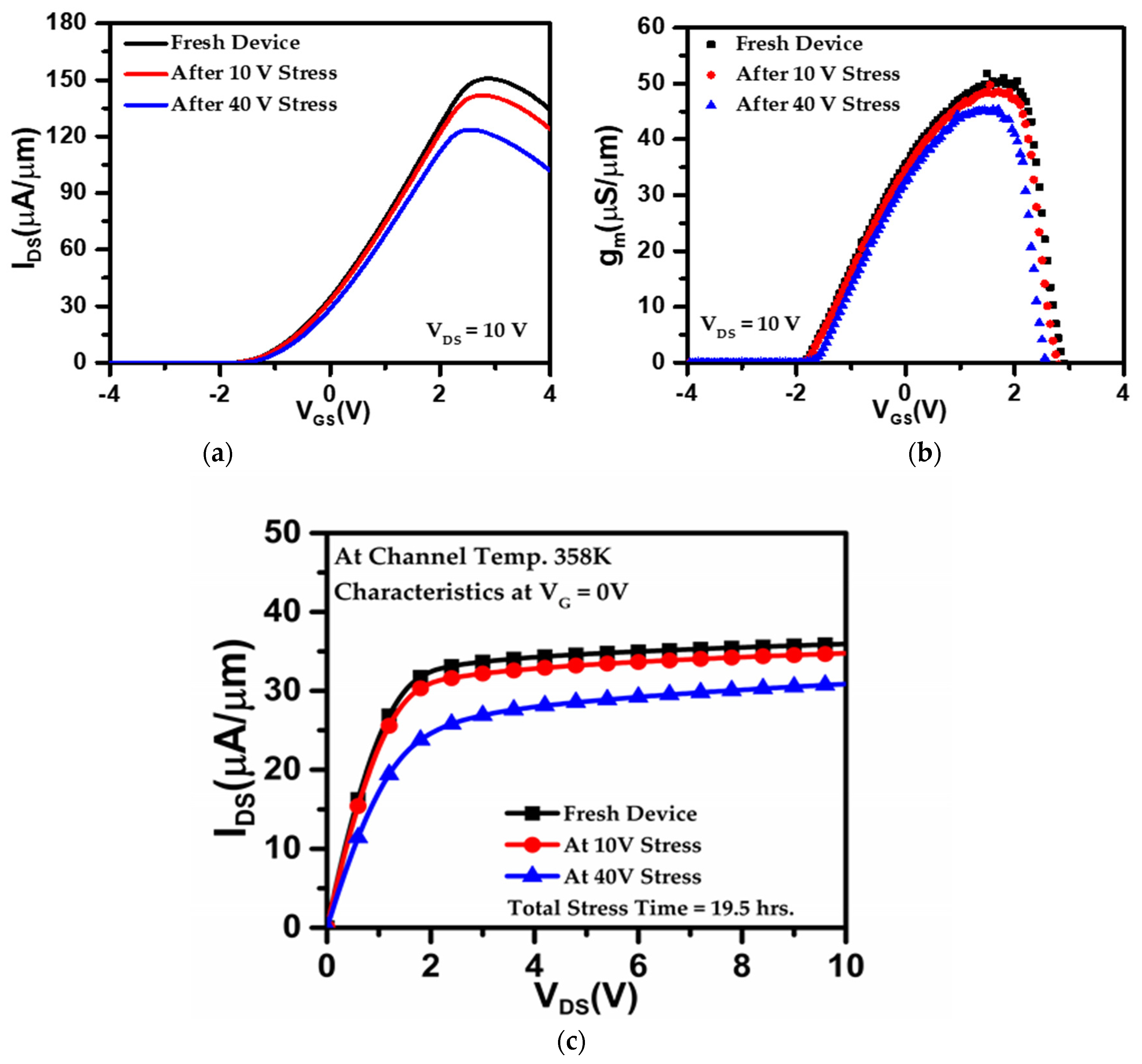
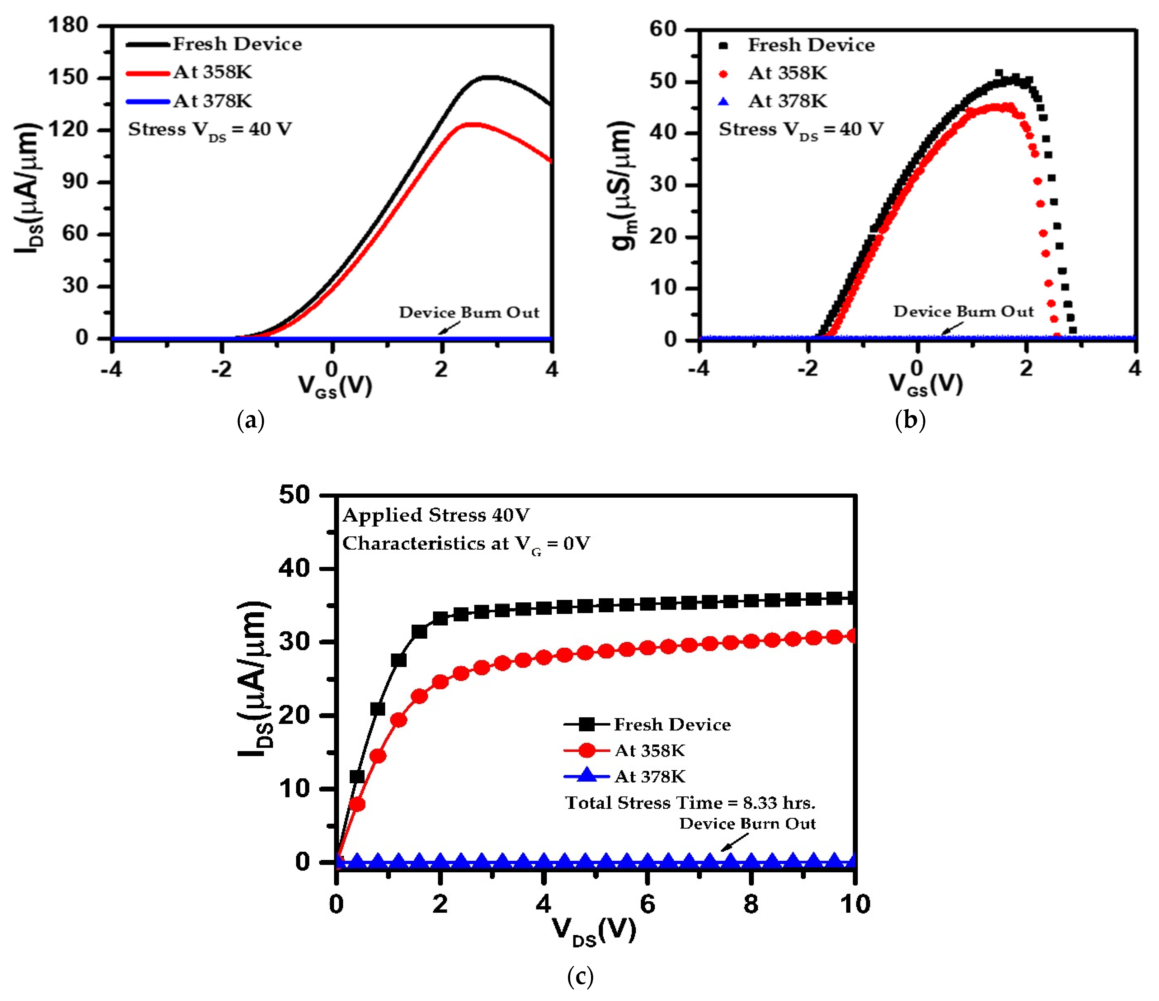
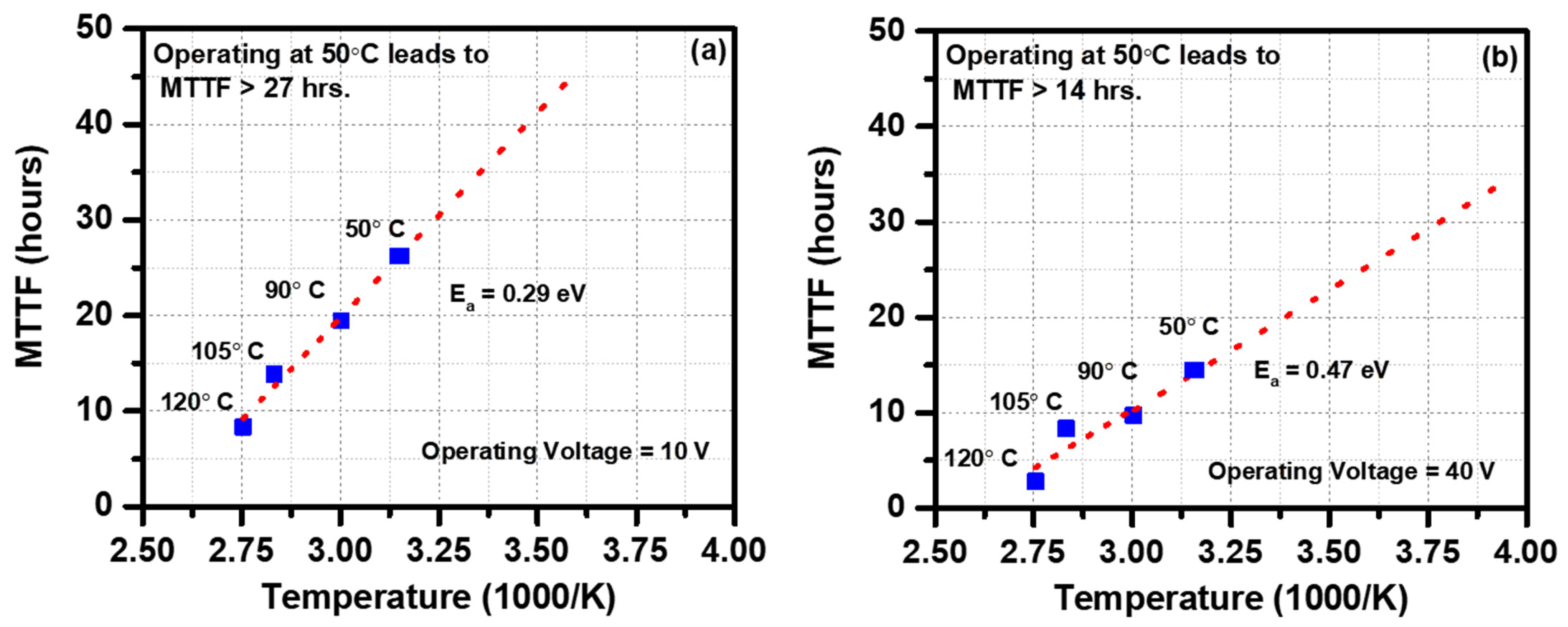
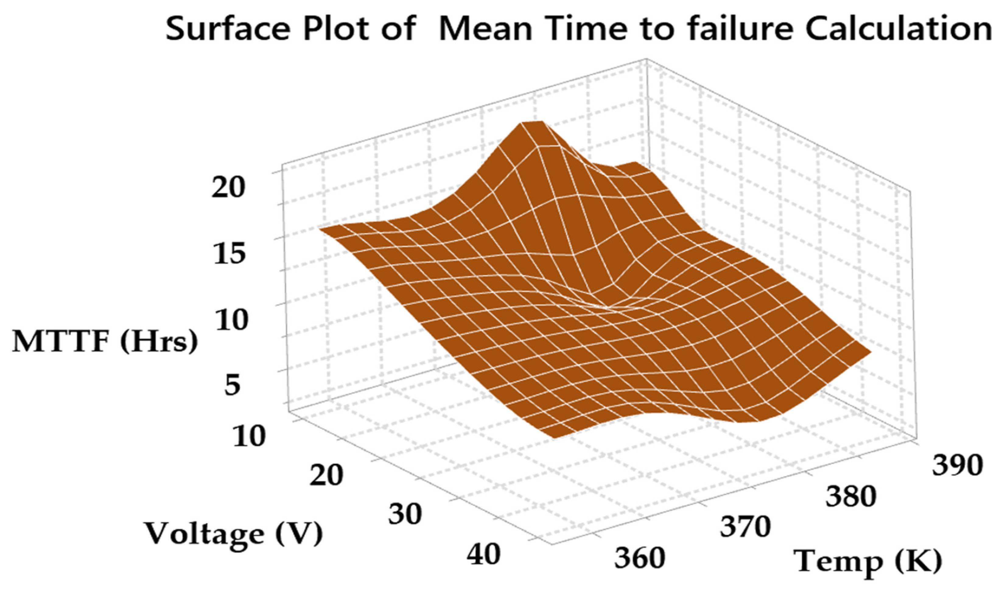
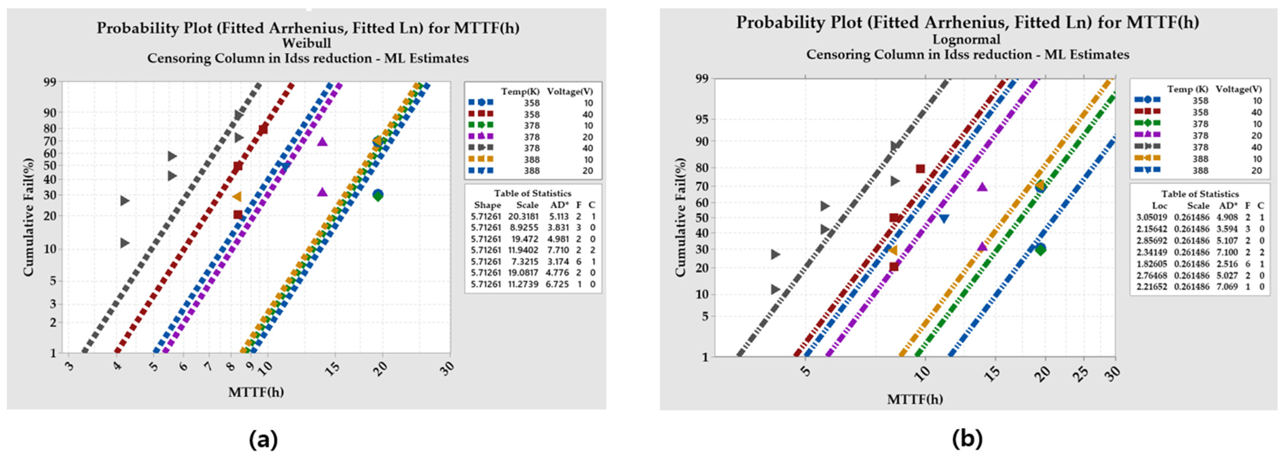
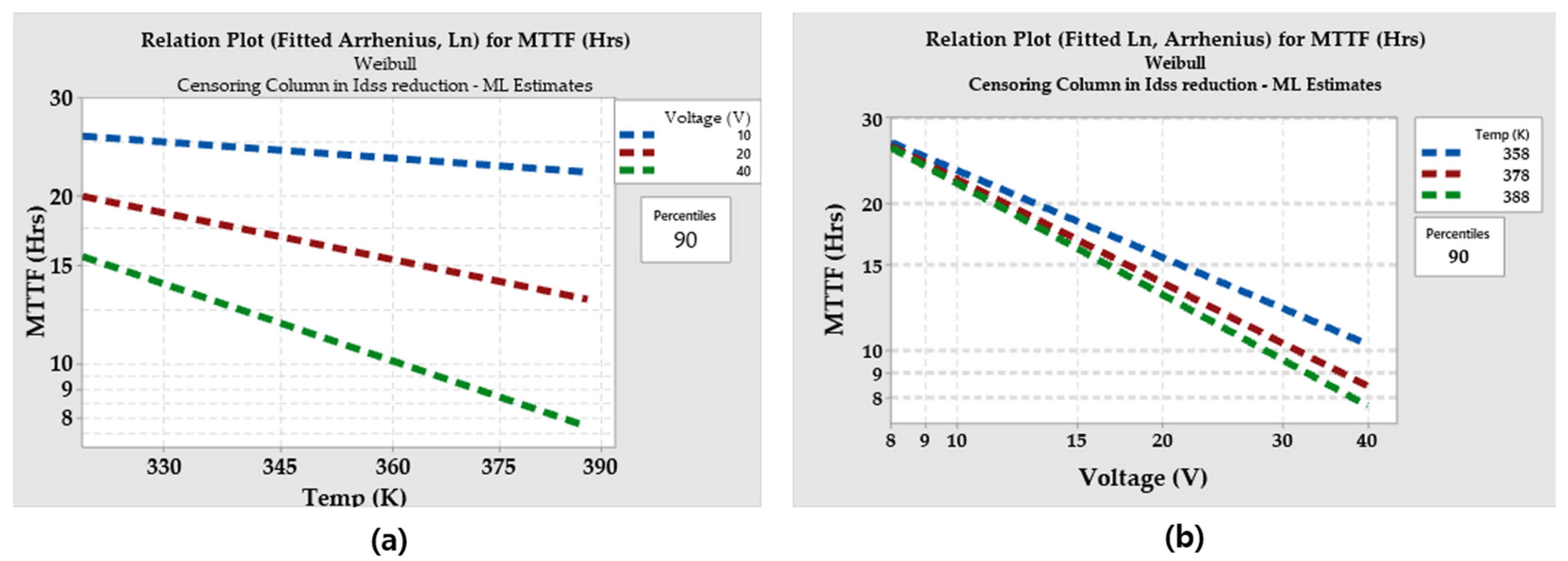
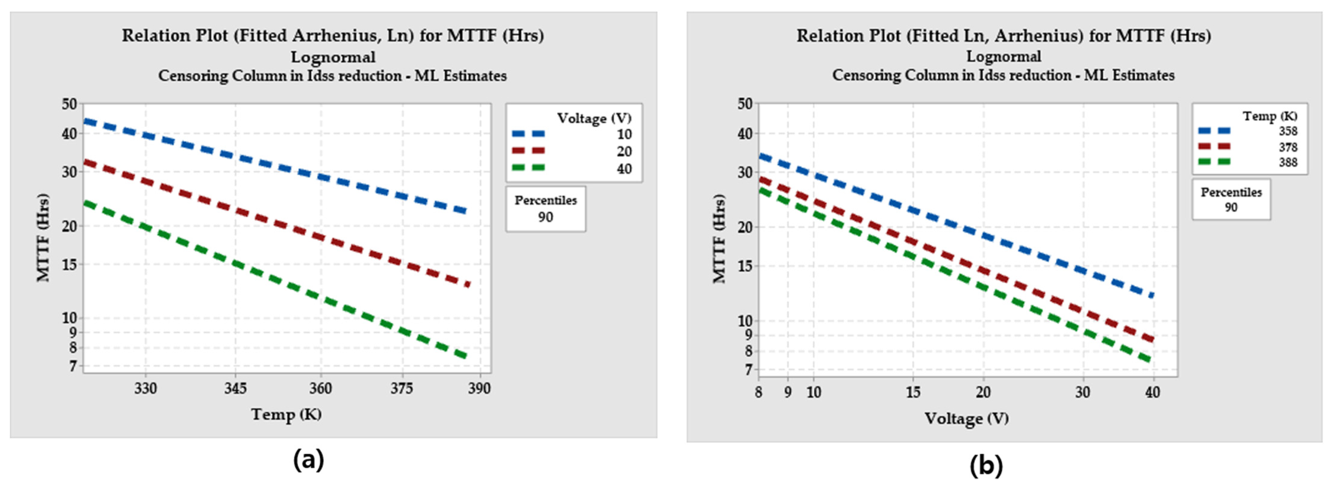
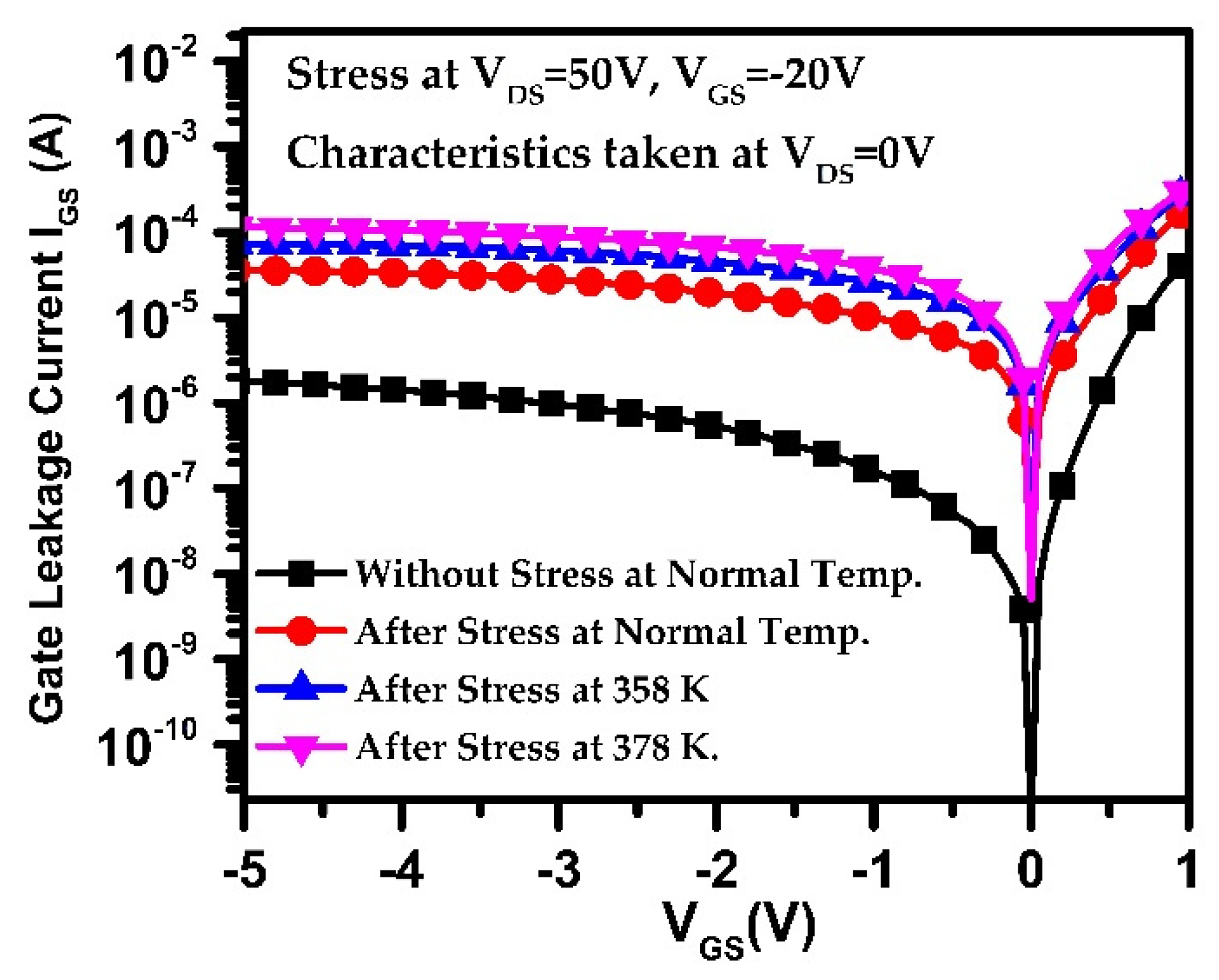
4. Results and Discussion

Figure 2b shows the output characteristics of the device at a channel temperature of 358 K under the open-channel condition Vgs = 0 V. Fresh device performance was also measured without any stress as 35 μA/μm in the saturation region. After applying 10 V of stress for 19.5 h, the output current drops by about 3.36%. Without changing the channel temperature, if 40 V of stress is applied to another device with the same gate length, then a 15% degradation of Idss is observed. The transfer characteristics (Figure 2a) of this device show similar drain current degradations. The transconductance (gm) degraded in a similar manner and consistency. On the other hand, tests were conducted with two different stress voltages (10 V and 40 V) separately on the same device at different channel temperatures. Figure 3 shows only two channel temperatures (358 K and 378 K) for the 40 V stress tests. The other tests show similar trends. Increasing the channel temperature to 378 K at 40 V stress completely burns out the device after 8.33 h. Owing to the high electric field and temperature, the device degraded critically. The parameter degradations for all temperatures and stresses are presented in Table 1.
Figure 4 shows the MTTF for each temperature in terms of the Arrhenius plot and reveals activation energies of 0.29 eV and 0.47 eV for operating voltages of 10 V and 40 V, respectively. When both curves are extrapolated to the typical temperature of 50 °C, MTTF values exceeding 25 h and 15 h are predicted. Lifetime degradations are observed when the operating voltage conditions are changed. Therefore, using only the operating voltage condition is insufficient for predicting the MTTF values of AlGaN/GaN devices. The calculated activation energy according to the Arrhenius plot increases by 0.2 eV, thus enhancing the voltage condition.
In Figure 5, separate experimental results are shown when varying two different channel temperatures to observe the voltage as an acceleration factor. Operating channel temperatures of 358 K and 378 K at three different voltage conditions (10 V, 20 V, and 40 V) are used to predict the MTTF values at 8 V as exceeding 26 h and 10 h, respectively. The voltage acceleration factors (γ) calculated from the power law are 0.028 and 0.023 for the two temperatures. The voltage acceleration factor thus decreases when the operating channel temperature increases.
The total surface plot of the MTTF calculations are presented in a 3D format in Figure 6. This graph represents a part of our experimental results. Plotting the operating voltage along the X-axis, the operating channel temperature along the Y-axis, and MTTF (h) along the Z-axis presents an apparent picture of the MTTF; this graph shows the real picture according to the Eyring model for multiple stresses and channel temperature values affecting MTTF calculations. At a moderate voltage value (between 20 V and 30 V) for a temperature of 380 K, the failure mode of the device is observed to fluctuate more. Normally, at low voltages (less than 10 V), the MTTF values exceed 15 h. Theoretically, at 360 K and 10 V, the device’s MTTF should be at its highest (maxima point). MTTF should be low at 390 K and 40 V (Minima). Practically, the device characteristics vary from one device to another. In Figure 6, at a 380 K temperature and at the corresponding 10 V and 20 V, respectively, both maxima and minima were found, respectively. At 380 K at 20 V, early device degradation was found, which is rarely found at other temperatures. We use two distributions, namely the Weibull and log-normal distributions, to calculate the cumulative failure (%) of the devices using Minitab software. These results are depicted in Figure 7. The relationships between the accelerating factors of temperature (K) and voltage (V), as well as Ln (Power), are shown for the Arrhenius model. The devices with Idss reductions that exceed 15% have a count value of 1 and those with reductions below 15% have a count of 0 in the censoring data.
Table 2 showing the results of 22 devices, according to their failure times for three different channel temperatures and operating voltages for each one. In both distributions, the estimation method used is the maximum likelihood criterion. At each accelerating level, the software uses the Anderson–Darling (adjusted) goodness-of-fit, and the simulated results of the two test criteria are shown in Figure 8. The two plots show completely different MTTF values. In Figure 8b, at a low voltage level, the temperature effects are low, such that increasing the channel temperature does not change the MTTF much. Considering only the operating voltage as the acceleration factor is thus misleading for calculating the MTTF. The confidence level is considered as the 90% interval. The other distribution (log-normal) shows slightly different results. Figure 7b shows the log-normal distributions of the same samples, and the simulated results of the separate tests are plotted in Figure 9.
The log-normal distributions show better fit than the Weibull distributions, with the MTTF values predicted to be greater than 40 h at low voltage conditions. The MTTF estimations in Figure 9b show slightly reduced values at low voltage conditions. We have thus calculated the MTTF values for non-commercial GaN devices that can be further applied to commercial devices.
We observed sudden degradations in the devices and therefore focused on analysis of the gate leakage current characteristics [30,31]. In this experiment, the devices were stressed in the deep-pinched-off region (Vds = 50 V, Vgs = −20 V) (Figure 10). At ambient temperature, the forward gate current towards Vg = 0 V increases after deterioration. Then, a gate leakage path developed through the interface states during the stress tests, as indicated by the increase in gate current. The forward gate current increases before the stress test around 0 V in the high-temperature measurements. Thus, the gate leakage path at high temperature could be the source of this degradation. Hence, this research suggests that evaluating gate leakage currents at ambient temperature could be used to screen for early device failures.

5. Conclusions

By considering both voltage and temperature as the acceleration factors for GaN device degradation, we demonstrate large shifts in the MTTF values. As the electric field/voltage is one of the dominant factors with respect to AlGaN/GaN HEMT devices, it cannot be ignored when calculating the MTTF values. Based on our experimental results, the log-normal distribution is an appropriate fit for the cumulative failure percentage and provides higher MTTF values than the Weibull distribution. Other experiments were performed through high-temperature reverse bias tests to show that early or premature failure could be caused by the gate leakage current.

Author Contributions

S.C. conducted all the experiments and wrote the manuscript, including preparation of the figures; T.-W.K. initiated the work, provided the main idea, and supervised the entire process. All authors analyzed and discussed the results. All authors have read and agreed to the published version of the manuscript.

Funding

This work was supported by the 2021 Research Fund of University of Ulsan.

Data Availability Statement

The data presented in this study are available on request from the corresponding author. The data are not publicly available due to privacy issues.

Conflicts of Interest

There are no conflict of interest.

References

  1. Mishra, U.K.; Shen, L.; Kazior, T.E.; Wu, Y.F. GaN-based RF power devices and amplifiers. Proc. IEEE 2008, 96, 287–305. [Google Scholar] [CrossRef]
  2. Palacios, T.; Chakraborty, A.; Rajan, S.; Poblenz, C.; Keller, S.; DenBaars, S.P.; Speck, J.S.; Mishra, U.K. High-power AlGaN/GaN HEMTs for Ka-band applications. IEEE Electron Device Lett. 2005, 26, 8–11. [Google Scholar] [CrossRef] [Green Version]
  3. Wu, Y.F.; Saxler, A.; Moore, M.; Smith, R.P.; Sheppard, S.; Chavarkar, P.M.; Wisleder, T.; Mishra, U.K.; Parikh, P. 30-W/mm GaN HEMTs by field plate optimization. IEEE Electron Device Lett. 2004, 25, 117–119. [Google Scholar] [CrossRef]
  4. Nuttinck, S.; Gebara, E.; Laskar, J.; Harris, M. Development of GaN wide bandgap technology for microwave power applications. IEEE Microw. Mag. 2002, 3, 80–87. [Google Scholar] [CrossRef]
  5. Jang, B.J.; Yom, I.B.; Lee, S.P. Millimeter wave MMIC low noise amplifiers using a 0.15 μm commercial pHEMT process. ETRI J. 2002, 24, 190–196. [Google Scholar] [CrossRef]
  6. Im, D.; Nam, I.; Lee, K. A low power broadband differential low noise amplifier employing noise and IM3 distortion cancellation for mobile broadcast receivers. IEEE Microw. Wirel. Compon. Lett. 2010, 20, 566–568. [Google Scholar] [CrossRef]
  7. Sun, H.; Alt, A.R.; Benedickter, H.; Feltin, E.; Carlin, J.; Gonschorek, M.; Grandjean, N.; Bolognesi, C.R. 205-GHz (Al,In)N/GaN HEMTs. IEEE Electron Device Lett. 2010, 31, 957–959. [Google Scholar] [CrossRef]
  8. del Alamo, J.A.; Joh, J. GaN HEMT reliability. Microelectron. Reliab. 2009, 49, 1200–1206. [Google Scholar] [CrossRef]
  9. Available online: www.wolfspeed.com (accessed on 6 December 2021).
  10. Available online: www.macom.com (accessed on 6 December 2021).
  11. Available online: www.qorvo.com (accessed on 6 December 2021).
  12. Meneghesso, G.; Rampazzo, F.; Kordoš, P.; Verzellesi, G.; Zanoni, E. Current collapse and high-electric-field reliability of unpassivated GaN/AlGaN/GaN HEMTs. IEEE Trans. Electron Devices 2006, 53, 2932–2940. [Google Scholar] [CrossRef]
  13. Cheney, D.J.; Douglas, E.A.; Liu, L.; Lo, C.F.; Xi, Y.Y.; Gila, B.P.; Ren, F.; Horton, D.; Law, M.E.; Smith, D.J.; et al. Reliability studies of AlGaN/GaN high electron mobility transistors. Semicond. Sci. Technol. 2013, 28, 074019. [Google Scholar] [CrossRef]
  14. Burnham, S.D.; Paine, B.M. Towards an RF GaN reliability standard. In Proceedings of the JEDEC Reliability of Compound Semiconductors Workshop, Indian Wells, CA, USA, 22 May 2017. [Google Scholar]
  15. Ohki, T.; Kikkawa, T.; Inoue, Y.; Kanamura, M.; Okamoto, N.; Makiyama, K.; Imanishi, K.; Shigematsu, H.; Joshin, K.; Hara, N. Reliability of GaN HEMTs: Current status and future technology. IEEE Int. Reliab. Phys. Symp. Proc. 2009, 61–70. [Google Scholar] [CrossRef]
  16. Matsushita, K.; Teramoto, S.; Sakurai, H.; Takada, Y.; Shim, J.; Kawasaki, H.; Tsuda, K.; Takagi, K. Reliability study of AlGaN/GaN HEMTs device. In Proceedings of the CS MANTECH Conference, Austin, TE, USA, 14–17 May 2007. [Google Scholar]
  17. Singhal, S.; Chaudhari, A.; Rajagopal, P.; Li, T.; Nagy, W.; Therrien, R.J. Qualification and reliability of a GaN process platform. In Proceedings of the CS MANTECH Conference, Austin, TE, USA, 14–17 May 2007. [Google Scholar]
  18. Jimenez, J.L.; Chowdhury, U. X-band GaN FET reliability. IEEE Int. Reliab. Phys. Symp. Proc. 2008, 429–435. [Google Scholar] [CrossRef]
  19. Chowdhury, U.; Jimenez, J.L.; Lee, C.; Beam, E.; Saunier, P.; Balistreri, T.; Park, S.Y.; Lee, T.; Wang, J.; Kim, M.J.; et al. TEM observation of crack- and pit-shaped defects in electrically degraded GaN HEMTs. IEEE Electron Device Lett. 2008, 29, 1098–1100. [Google Scholar] [CrossRef]
  20. Zanoni, E.; Meneghini, M.; Chini, A.; Marcon, D.; Meneghesso, G. AlGaN/GaN-based HEMTs failure physics and reliability: Mechanisms affecting gate edge and Schottky junction. IEEE Trans. Electron Devices 2013, 60, 3119–3131. [Google Scholar] [CrossRef]
  21. Cheney, D.J.; Douglas, E.A.; Liu, L.; Lo, C.F.; Gila, B.P.; Ren, F.; Pearton, S.J. Degradation mechanisms for GaN and GaAs high speed transistors. Materials 2012, 5, 2498–2520. [Google Scholar] [CrossRef]
  22. Meneghesso, G.; Verzellesi, G.; Danesin, F.; Rampazzo, F.; Zanon, F.; Tazzoli, A.; Meneghini, M.; Zanoni, E. Reliability of GaN high-electron-mobility transistors: State of the art and perspectives. IEEE Trans. Device Mater. Reliab. 2008, 8, 332–343. [Google Scholar] [CrossRef]
  23. Marcon, D.; Viaene, J.; Favia, P.; Bender, H.; Kang, X.; Lenci, S.; Stoffels, S.; Decoutere, S. Reliability of AlGaN/GaN HEMTs: Permanent leakage current increase and output current drop. In Proceedings of the 20th IEEE International Symposium on the Physical and Failure Analysis of Integrated Circuits (IPFA), Suzhou, China, 15–19 July 2013; pp. 249–254. [Google Scholar] [CrossRef]
  24. Saunier, P.; Lee, C.; Balistreri, A.; Dumka, D.; Jimenez, J.; Tserng, H.Q.; Kao, M.Y.; Chao, P.C.; Chu, K.; Souzis, A.; et al. Progress in GaN performances and reliability. In Proceedings of the 2007 65th Annual Device Research Conference, South Bend, IN, USA, 18–20 June 2007; pp. 35–36. [Google Scholar] [CrossRef]
  25. Lee, S.; Vetury, R.; Brown, J.D.; Gibb, S.R.; Cai, W.Z.; Sun, J.; Green, D.S.; Shealy, J. Reliability assessment of AlGaN/GaN HEMT technology on SIC for 48 V applications. IEEE Int. Reliab. Phys. Symp. Proc. 2008, 446–449. [Google Scholar] [CrossRef]
  26. Musallam, M.; Yin, C.; Bailey, C.; Johnson, M. Mission profile-based reliability design and real-time life consumption estimation in power electronics. IEEE Trans. Power Electron. 2015, 30, 2601–2613. [Google Scholar] [CrossRef]
  27. Fan, D.; Ren, Y.; Wang, Z.; Liu, L. Mission reliability prediction methods for board-level electronic equipment based on physics of failure and Bayesian networks. In Proceedings of the 2015 First International Conference on Reliability Systems Engineering (ICRSE), Beijing, China, 21–23 October 2015. [Google Scholar] [CrossRef]
  28. Kerber, A.; McMahon, W.; Cartier, E. Voltage ramp stress for hot-carrier screening of scaled CMOS devices. IEEE Electron Device Lett. 2012, 33, 749–751. [Google Scholar] [CrossRef]
  29. Chen, Y.H.; Ma, X.H.; Chen, W.W.; Hou, B.; Zhang, J.C.; Hao, Y. Influence of the gate edge on the reverse leakage current of AlGaN/GaN HEMTs. AIP Adv. 2015, 5, 097154. [Google Scholar] [CrossRef]
  30. Joh, J.; Xia, L.; del Alamo, J.A. Gate current degradation Mechanisms of GaN High Electron Mobility Transistors. In Proceedings of the IEEE Electron Device Meeting, Washington, DC, USA, 10–12 December 2007; pp. 385–388. [Google Scholar] [CrossRef]
  31. Mimouni, A.; Fernández, T.; Rodriguez-Tellez, J.; Tazon, A.; Baudrand, H.; Boussuis, M. Gate leakage current in GaN HEMT’s: A degradation modeling approach. Electr. Electron. Eng. 2013, 2, 397–402. [Google Scholar] [CrossRef] [Green Version]
Figure 1. Cross-sectional diagram of the AlGaN/GaN structure used for MTTF experiments.
Electronics 10 03052 g001
Figure 2. (a,b) Transfer characteristics shown for different stressed conditions of the device at a fixed channel temperature of 358 K. (c) Output characteristics demonstrated based on 15% Idss degradation of the device and total stressed time of 19.5 h.
Electronics 10 03052 g002
Figure 3. (a,b) Transfer characteristics of the device stressed at 40 V at two channel temperatures result in transconductance degradations at different channel temperatures; similar trends as in (c) are observed for the output characteristics.
Electronics 10 03052 g003
Figure 4. (a) MTTF calculation based on operating voltage of 10 V results in activation energy Ea = 0.29 eV. (b) MTTF calculation based on operating voltage of 40 V results in activation energy Ea = 0.47 eV. Both graphs predict the extrapolated results when the device is operated at 50 °C.
Electronics 10 03052 g004
Figure 5. (a) MTTF calculation based on channel temperature of 358 K results in voltage acceleration factor γ = 0.028. (b) MTTF calculation based on channel temperature of 378 K results in voltage acceleration factor γ = 0.023. Both graphs predict the extrapolated results when the device is operated at 8 V.
Electronics 10 03052 g005
Figure 6. Eyring model representation in 3D graph for two different acceleration factors dominating device degradation.
Electronics 10 03052 g006
Figure 7. (a) Weibull distribution of MTTF values; (b) log-normal distribution of MTTF values.
Electronics 10 03052 g007
Figure 8. Weibull distributions for calculated (a) voltage and (b) channel temperature MTTF values at the 90% confidence level.
Electronics 10 03052 g008
Figure 9. Log-normal distributions for calculated (a) voltage and (b) channel temperature MTTF values at the 90% confidence level.
Electronics 10 03052 g009
Figure 10. Gate leakage characteristics analysis at different temperatures to investigate sudden device failure.
Electronics 10 03052 g010
Table 1. Parameter degradations for different gate voltages (at a constant channel temperature of 358 K).
ParametersVoltage = 10 VVoltage = 40 V
Saturation current (Idss (μA/μm))3.36%14%
Transconductance
(gm (μS/μm))
5%10%
On resistance
(Ron (Ω/μm))
5.6%46%
Table 2. Part of the experimental results.
Temperature (K)Voltage (V)MTTF (h)Idss Reduction (%)
Censor
358108.300
1019.401
1019.401
2014.231
209.100
2011.531
408.301
409.721
408.301
3781019.401
1019.441
202.770
2013.891
202.770
2013.881
404.171
405.560
402.770
408.311
408.301
3881019.401
108.331
2011.111
40Device damagedN/A
Publisher’s Note: MDPI stays neutral with regard to jurisdictional claims in published maps and institutional affiliations.

