Communication

A Low-Cost and Efficient Microstrip-Fed Air-Substrate-Integrated Waveguide Slot Array

Electrical and Computer Engineering Department, The University of Alabama, Tuscaloosa, AL 35487, USA
*
Author to whom correspondence should be addressed.
Electronics 2021, 10(3), 338; https://doi.org/10.3390/electronics10030338
Submission received: 5 January 2021 / Revised: 27 January 2021 / Accepted: 29 January 2021 / Published: 1 February 2021
(This article belongs to the Special Issue Antennas in the 5G System)

Abstract

:
A microstrip-fed air-substrate-integrated waveguide (ASIW) slot array with high efficiency and low cost is presented. The design cuts out the substrate material within SIW, replaces the vias with metallic sidewalls, and uses a simple microstrip line-waveguide transition to feed the slot array. Radiating slots are cut on a 5-mil brass-plate, which covers the top of the substrate cutout to resemble a hollow waveguide structure. This implementation provides a simple and efficient antenna array solution for millimeter-wave (mm-wave) applications. Meanwhile, the fabrication is compatible with the standard printed circuit board (PCB) manufacturing process. To demonstrate the concept, a 4-element ASIW slot array working at the n257 band for 5G communications was designed using low-cost Rogers 4350B and FR4 substrate materials. Our simulation result shows 18% more efficiency than a conventional SIW slot array using the same substrate. The fabricated prototype shows |S11| < −15 dB over 27–29 GHz and a peak realized gain of 10.1 dBi at 28.6 GHz. The design procedure, prototyping process, and design analysis are discussed in the paper.

1. Introduction

With the rapid development of 5G communication systems and mm-wave automotive radars, better quality, low-cost, and low-loss antennas are in high demand. Substrate-integrated waveguide (SIW), which was first introduced by Deslandes and Wu [1], provides a high-performance solution for mm-wave antenna design. Since then, SIW slot arrays have been analyzed and developed at multiple bands for different applications [2,3,4,5]. They are compact and easy to fabricate and integrate with other planar circuits. However, the SIW slot arrays suffer from different sources of loss such as conductor loss, dielectric loss, and wave-leakage loss, which become more significant as frequency goes beyond K-band. Building high-efficiency antennas at mm-wave requires expensive low-loss substrate materials and high-precision manufacturing processes. To overcome these limits, the air-filled structure of the traditional rectangular waveguide has been reconsidered and gradually implemented using the current substrate-integrated circuit (SIC) technique. The numerical analysis in Ranjkesh et al. [6] shows that when using Rogers RO4003 (Rogers Corporation, Chandler, Arizona) as the substrate, the attenuation constant of SIW with an air-cut is reduced by more than 1.5 Np/m at 29 GHz, compared to that of SIW. More recently, an air-filled SIW (AFSIW) [7] and a slot array using this structure [8] were developed. The simulated antenna array has an efficiency of more than 90%, which benefits from the substrate cut-out and the efficient transition from SIW and AFSIW. However, a part of the waveguide is dielectric-filled. Additionally, the gaps between existing metallic vias can still cause wave-leakage and reduce antenna performance at higher mm-wave frequencies. To eliminate the metallic vias, simplify the transition, and further improve the antenna efficiency, we introduce a tapered microstrip-fed air-SIW (ASIW) slot array with copper-plated side walls. The radiating slots are cut on a 5-mil brass layer, which covers the top of the substrate cutout. The copper-plated sidewalls along with the top and bottom metallic covers form a hollow waveguide with no dielectric material and no vias. This three-layer structure can be easily aligned with alignment holes and fabricated with the current multi-layer PCB manufacturing process. This paper will be arranged as follows. The antenna array design and fabrication process are discussed in Section 1 and Section 2. The simulated and measured antenna performance, the effect of surface roughness on antenna efficiency, and a comparison between the proposed ASIW slot array and the SIW slot array using the same substrate material are presented in Section 3. Finally, the conclusion is given in Section 4.

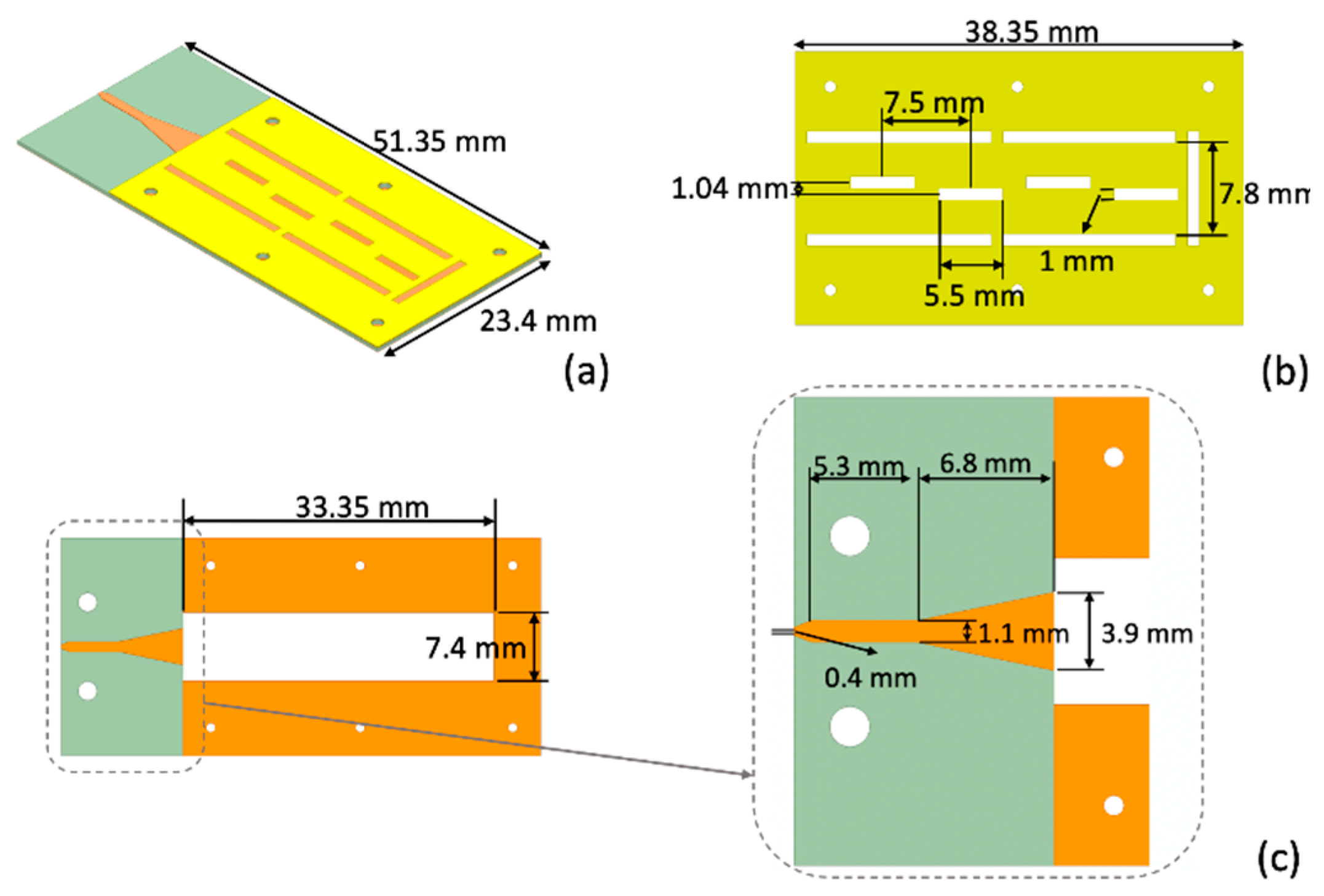
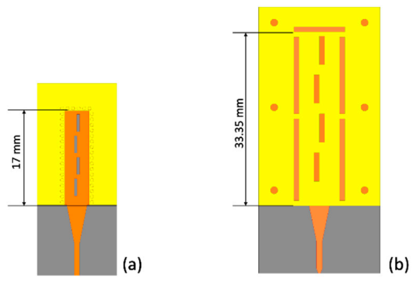
2. Antenna Array Design

The 3-dimensional (3D) structure of the proposed 1 × 4 slot array is shown in Figure 1a. The printed circuit board (PCB) multilayer stack-up is shown in Figure 1b.
The top layer is a 5-mil brass plate. Its conductivity ( σ ) is only 28% that of copper. Despite its lower conductivity, brass is much less prone to oxidation and the increased amount of zinc can provide the material with improved strength, which is mechanically more stable than most 5-mil substrates. Additionally, for waveguide structures with a large conductor area, simulation results show that a brass-based waveguide only has 4% higher attenuation at 30 GHz than the copper counterpart (Figure 2).
In our design, the brass-plate has four radiating slots in the middle, six alignment holes on the sides to ensure accurate placement, and five additional slots around the waveguide for soldering. These additional slots are only used for prototyping, which can be eliminated in the actual manufacturing process with proper conductive bonding or mechanical assembly. The purpose of soldering slots surrounding the waveguide instead of using screws is to improve the prototyping accuracy. Although the 5-mil brass plate is stronger than copper and most 5-mil substrates, this thin layer is still susceptible to bending. There can be small air gaps between adjacent screws that can cause wave leakage and reduce antenna efficiency. The middle layer includes a microstrip line (MSL) and a hollow waveguide, which are fabricated on a 20-mil Rogers RO4350B substrate (Rogers Corporation, Chandler, Arizona). RO4350B has a relative permittivity ( ε r ) of 3.66 and a dielectric loss tangent ( t a n δ ) of 0.0037, which provide a good performance at high frequencies with a relatively low cost. The MSL is gradually tapered to allow the quasi-TEM mode to smoothly transition into TE10 mode of the waveguide. To avoid short-circuiting the input of the waveguide, only three edges of the waveguide are copper plated as shown in Figure 1a. The top layer of the bottom substrate serves as the ground, and thus other low-cost material may be chosen. Since the waveguide shares the same physical structure as the hollow rectangular waveguide, the width a of the waveguide can be simply determined by
a =   c 2 f c ,
In which c is the speed of light in free space and f c is the TE10 mode cutoff frequency, which is 20.27 GHz in this design. The detailed dimensions of the design are shown in Figure 3.

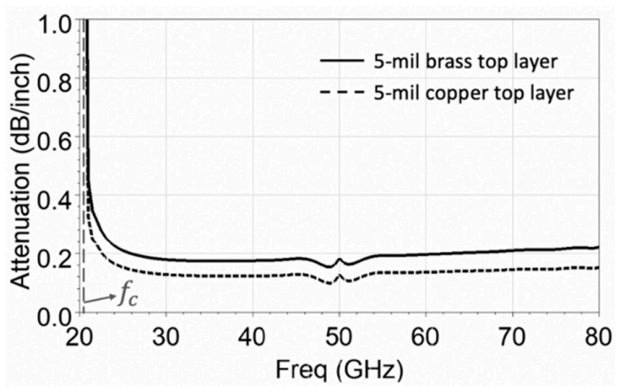
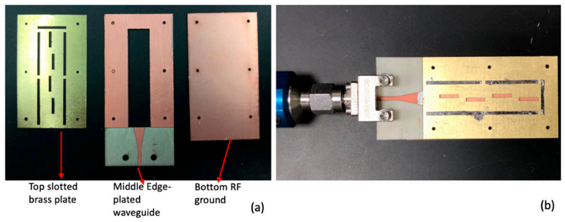
3. Antenna Array Fabrication

The individually milled layers and the assembled prototype are shown in Figure 4.
For prototyping, the radiating slots on the brass-plate, the waveguide, and microstrip lines were cut and milled using LPKF Proto Laser S4 (LPKF Laser and Electronics, Garbsen, Germany). After cutting, the edges of the waveguide were copper-plated using an LPKF Contac S4 plating machine (LPKF Laser and Electronics, Garbsen, Germany). To plate only three edges of the waveguide, the RO4350B substrate was cut to form a five-sided hollow polygon as shown in Figure 5.
After copper-plating, the protruding small triangle was cut out so that the input edge of the waveguide was not covered with copper. For the prototype, all the layers were aligned and soldered manually in the lab. Additionally, the surface roughness of the in-house plated copper layer could be much higher than the specification. These fabrication inaccuracies can be reduced with the standard PCB manufacturing process. To characterize the antenna efficiency more accurately, the effect of surface roughness will be discussed in the next section.

4. Results and Discussion

4.1. Simulated and Measured Antenna Performance

The ASIW slot array is simulated and analyzed in ANSYS Electronics Desktop (Canonsburg, PA, USA). The fabricated antenna is characterized in our anechoic chamber. As shown in Figure 6, the electric field of TE10 mode is uniformly distributed inside the ASIW with radiating slots.
The measured and simulated reflection coefficients and realized gain are shown in Figure 7. In the simulation, the surface roughness of copper and brass layers is considered. The fabricated array has an impedance bandwidth (where |S11| −10 dB) of 10.3% (26.7–29.6 GHz). Within this bandwidth, the measured realized gain is 7.6–10.1 dBi, which is slightly less than the simulation results especially at higher frequencies. This difference is mainly caused by the non-perfect surface roughness model, which will be discussed in Section 4.2.
In Figure 8, the measured and simulated radiation patterns at 27 GHz, 28 GHz, and 29.5 GHz are normalized and plotted. Both E-plane and H-plane radiation patterns agree well with the simulation results. Besides, the slot array maintains a centered main beam from 27 GHz to 29.6 GHz with a maximum of 3° tilting at 27 GHz. This ensures a wide range of frequency scanning required by modern wireless communications.
For the efficiency calculation of both measured and simulated array, the reference plane is set to the input of the end-launch connector. Thus, return loss caused by impedance mismatch, as well as surface roughness, dielectric, and conductor loss of the MSL section, is considered. When the MSL section is de-embedded and the reference plane is set to the input of waveguide, simulated antenna efficiency is as high as 98%. However, to evaluate the antenna performance when integrating with planar circuits, the effect of the MSL section has to be considered. By taking the ratio of total radiated power over incident power, the measured efficiency is 84% at 28.6 GHz, which is 4% lower than the simulated efficiency of 88% with the consideration of surface roughness (RRMS). This reduction is mainly caused by two factors. One is the fabrication error mentioned in Section 3, the other is the limitation of surface roughness model. When RRMS = 0, the simulated total efficiency is 92% as shown in Figure 9, causing a larger discrepancy between simulated and measured results.

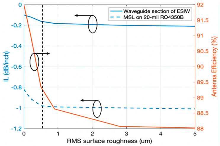
4.2. Surface Roughness Model

The surface roughness model used in the simulation is based on Groisse et al. [9], who described a factor CS for correcting power loss (PL) caused by RRMS
P L r o u g h = P L s m o o t h   ×   C S   ,
C S = 1 + exp δ 2 R R M S 1.6   ,
In the equations, PLrough is the power loss through a rough conductor, PLsmooth is the power loss through a smooth conductor, and δ is the skin depth. This correction factor works well for conductors with moderate surface roughness. As RRMS and frequency increases, CS will saturate at two. This also means the maximum power loss caused by RRMS is only twice the smooth conductor.
To evaluate the surface roughness effect on the ASIW slot array performance using Groisse’s model, the antenna efficiency and insertion loss (IL) of MSL and air-filled waveguide versus RRMS are plotted in Figure 9.
Because the waveguide is filled with air, the loss is mainly caused by the MSL section. When RRMS is lower than 0.6 µm, the IL increases; antenna efficiency decreases linearly with higher RRMS, while they start to saturate when RRMS is higher than 1 µm. However, in real measurement, this saturation will not occur and the insertion loss for rough conductors at high frequencies can be substantially higher than the calculated one [10]. For our array prototype, a low-cost RO4350B with electrodeposited (ED) copper was used, which gave us an RRMS of 2.8 µm. The in-house copper-plating process could have also produced a higher RRMS. These could have been the main causes of the lower measured efficiency and were not predicted by Groisse’s model. This result also confirms that the ASIW slot array fabricated on a low-cost substrate material can have improved efficiency with better surface treatment, such as reversed treated ED copper (RRMS = 9 µm) and standard copper plating techniques.

4.3. Antenna Performance Comparison

With the existence of the well-developed SIW slot array, the purpose of the proposed ASIW slot array is to produce better antenna efficiency with a lower budget. For comparison, a SIW slot array using the same 20-mil Rogers RO4350 (Rogers Corporation, Chandler, Arizona) was designed. Both arrays were optimized to the similar operating frequencies, and their reflection coefficients and efficiencies are shown in Figure 10a.
The SIW slot array has 30% less bandwidth than the ASIW slot array. Although they have a similar level of reflection coefficient at 27.6 GHz, the efficiency of the ASIW slot array is 18% higher than that of the SIW slot array. Furthermore, the hollow waveguide structure of ASIW can provide a much larger aperture size than the dielectric-filled SIW, as shown in Figure 11.
This larger aperture of the 1 × 4 SIW slot array provides a 3.7 dB higher gain and a 58% narrower H-plane half-power beamwidth (HPBW) than the 1 × 4 SIW slot array as shown in Figure 10b. These can be beneficial for some mm-wave applications. To achieve the same gain and beamwidth, the SIW slot array would have to have a longer dielectric-filled waveguide and more radiating slots. This would result in even higher dielectric loss within the waveguide.
The performance of ASIW slot array is also compared to other works, as shown in Table 1. As discussed before, the realized gain and total efficiency of the ASIW array not only include the impedance mismatch and connector loss but also dielectric, conductor, and surface roughness loss of the MSL feeding. When these effects are de-embedded by setting the reference plane to the input of the waveguide as described in Parment et al. [8], the simulated antenna efficiency of ASIW slot array is 98% and the realized gain is 11.3 dBi at 29.5 GHz. Compared to AFSIW, the advantage of proposed ASIW is more pronounced at higher mmWave frequencies, since the densely placed vias of AFSIW are replaced with metallic walls, which can be more accurately fabricated. The ESIW slot array presented in Qi et al. [11] does not suffer from the loss of planar transition, because the waveguide is directly fed by a 2.4 mm connector, which makes it incompatible with planar circuit fabrication technologies. Overall, the proposed ASIW slot array can achieve a high efficiency with a wide bandwidth. Meanwhile, the array can still be integrated with other planar circuits using the MSL to waveguide transition.

5. Conclusions

A high-efficiency and low-loss ASIW slot array design is proposed in this paper. The hollow waveguide implementation with a simple tapered MSL feeding eliminates the substrate loss and wave-leakage loss existing in the conventional SIW slot arrays. The proposed four-element array covering the 28GHz 5G band shows 18% higher efficiency than the SIW slot array designed on the same substrate. During the analysis, surface roughness has a major contribution to the loss of the ASIW slot array. With low-roughness surface treatment, higher antenna efficiency can be achieved with low-cost substrate materials.

Author Contributions

Conceptualization, J.-B.Y. and L.L.; methodology, L.L. and J.-B.Y.; software, L.L. and J.-B.Y.; validation, L.L.; formal analysis, L.L.; investigation, L.L. and J.-B.Y.; resources, L.L. and J.-B.Y.; data curation, L.L.; writing—original draft preparation, L.L.; writing—review and editing, L.L. and J.-B.Y.; visualization, L.L.; supervision, J.-B.Y.; project administration, J.-B.Y.; funding acquisition, J.-B.Y. All authors have read and agreed to the published version of the manuscript'

Funding

This research was funded by The University Corporation for Atmospheric Research (UCAR): National Oceanic and Atmospheric Administration (NOAA), grant number 26548 and Aerotenna, Inc. grant number 25929.

Institutional Review Board Statement

Not applicable.

Informed Consent Statement

Not applicable.

Data Availability Statement

The data presented in this study are available on request from the corresponding author.

Conflicts of Interest

The authors declare no conflict of interest.

References

  1. Deslandes, D.; Wu, K. Integrated microstrip and rectangular waveguide in planar form. IEEE Microw. Wirel. Compon. Lett. 2001, 11, 68–70. [Google Scholar] [CrossRef]
  2. Yan, L.; Hong, W.; Hua, G.; Chen, J.; Wu, K.; Cui, T.J. Simulation and experiment on SIW slot array antennas. IEEE Microw. Wirel. Compon. Lett. 2004, 14, 446–448. [Google Scholar] [CrossRef]
  3. Ding, Y.; Wu, K. A 4 × 4 Ridge Substrate Integrated Waveguide (RSIW) Slot Array Antenna. IEEE Antennas Wirel. Propag. Lett. 2009, 8, 561–564. [Google Scholar] [CrossRef]
  4. Navarro, D.V.; Carrera, L.F.; Baquero, M. A SIW slot array antenna in Ku band. In Proceedings of the Fourth European Conference on Antennas and Propagation, Barcelona, Spain, 12–16 April 2010; pp. 1–4. [Google Scholar]
  5. Xu, J.; Chen, Z.N.; Qing, X.; Hong, W. 140-GHz TE20-Mode Dielectric-Loaded SIW Slot Antenna Array in LTCC. IEEE Trans. Antennas Propag. 2012, 61, 1784–1793. [Google Scholar] [CrossRef]
  6. Ranjkesh, N.; Shahabadi, M. Reduction of dielectric losses in substrate integrated waveguide. Electron. Lett. 2006, 42, 1230–1231. [Google Scholar] [CrossRef]
  7. Parment, F.; Ghiotto, A.; Vuong, T.-P.; Duchamp, J.-M.; Wu, K. Air-Filled Substrate Integrated Waveguide for Low-Loss and High Power-Handling Millimeter-Wave Substrate Integrated Circuits. IEEE Trans. Microw. Theory Tech. 2015, 63, 1228–1238. [Google Scholar] [CrossRef]
  8. Parment, F.; Ghiotto, A.; Vuong, T.-P.; Duchamp, J.-M.; Wu, K. Millimetre-wave air-filled substrate integrated waveguide slot array antenna. Electron. Lett. 2015, 53, 704–706. [Google Scholar] [CrossRef]
  9. Groiss, S.; Bardi, I.; Biro, O.; Preis, K.; Richter, K. Parameters of lossy cavity resonators calculated by the finite element method. IEEE Trans. Magn. 1996, 32, 894–897. [Google Scholar] [CrossRef]
  10. Horn, A.F.; Reynolds, J.W.; LaFrance, P.A. Sonnet Software: Effect of Conductor Profile on the Insertion Loss, Phase Constant, and Dispersion in Thin High Frequency Transmission Lines. Available online: https://www.sonnetsoftware.com/support/downloads/publications/5-TA1_Al_Horn.pdf (accessed on 9 January 2020).
  11. Qi, Z.; Li, X.; Xiao, J.; Zhu, H. Low-Cost Empty Substrate Integrated Waveguide Slot Arrays for Millimeter-Wave Applications. IEEE Antennas Wirel. Propag. Lett. 2019, 18, 1021–1025. [Google Scholar] [CrossRef]
  12. Xu, J.; Chen, Z.N.; Qing, X. CPW Center-Fed Single-Layer SIW Slot Antenna Array for Automotive Radars. IEEE Trans. Antennas Propag. 2014, 62, 4528–4536. [Google Scholar] [CrossRef]
  13. Miralles, E.; Belenguer, A.; Matéo, J.; Torres, A.; Esteban, H.; Borja, A.L.; Boria, V.E. Slotted ESIW antenna with high efficiency for a MIMO radar sensor. Radio Sci. 2018, 53, 605–610. [Google Scholar] [CrossRef]
Figure 1. (a) Exploded view of air-substrate-integrated waveguide (ASIW) slot array; (b) printed circuit board (PCB) laminated structure of ASIW slot array.
Electronics 10 00338 g001
Figure 2. Attenuation of ASIW with a 5-mil brass top layer ( σ = 1.5 ×   10 7   S / m ) and a 5-mil copper top layer ( σ = 5.8 ×   10 7   S / m ). The root mean square (RMS) surface roughness is set to 1 for both materials.
Electronics 10 00338 g002
Figure 3. Dimensions of the 28 GHz ASIW slot array. (a) Overall size (b) Dimensions of the 5-mil top slotted brass plate (c) Dimensions of the waveguide and microstrip line (MSL)-waveguide transition.
Electronics 10 00338 g003
Figure 4. (a) Fabricated individual layers before assembly; (b) assembled prototype of proposed ASIW slot array under test.
Electronics 10 00338 g004
Figure 5. Three-edged copper plating process. The small triangle is cut after copper plating, such that the MSL-waveguide transition is not short-circuited.
Electronics 10 00338 g005
Figure 6. Electric-field distribution on the MSL and inside the ASIW with radiating slots at 28 GHz.
Electronics 10 00338 g006
Figure 7. Simulated and measured peak realized gain and reflection coefficient of ASIW slot array.
Electronics 10 00338 g007
Figure 8. Simulated and measured radiation patterns (E-plane and H-plane) of ASIW slot array at 27 GHz, 28 GHz, and 29.5 GHz.
Electronics 10 00338 g008
Figure 9. Simulated insertion loss (IL) and antenna efficiency versus RMS surface roughness at 28 GHz using Groisse’s surface roughness model.
Electronics 10 00338 g009
Figure 10. Comparison between ASIW slot array and substrate-integrated waveguide (SIW) slot array optimized to the similar frequency range using the same 20-mil Rogers RO4350B (Rogers Corporation, Chandler, Arizona) substrate. (a) Total antenna efficiency and |S11| of ASIW slot array and SIW slot array. (b) Peak realized gain and half-power beamwidth (HPBW) of ASIW slot array and SIW slot array.
Electronics 10 00338 g010
Figure 11. Size comparison between SIW slot array and ASIW slot array optimized to the similar frequency range using the same 20-mil RO4350B material. (a) SIW slot array; (b) ASIW slot array.
Electronics 10 00338 g011
Table 1. Comparison between different SIW slot array technologies.
Slot Array
Type
Realized Gain (dBi)Number of ElementsCenter
Frequency
(GHz)
Efficiency Fractional   Bandwidth   ( | S 11 |   10 dB ) Compatibility with Planar Circuits
SIW [2]15.7 4 × 4 10.0n.a.6%Yes
SIW [12]22.8 4 × 32 24.067%1.7%Yes
AFSIW [8]11.5 1 1 × 4 30.597.4% 1,28.7%Yes
ESIW with Cavity Loading [11]15.5 1 × 6 38.590.7%12.7%No
ESIW [13]15 1 × 10 16.2590.78%4.3%Yes
ASIW (this work)10.1 (11.3 1,2) 1 × 4 28.1584% 3 (98% 1,2)10.7%Yes
1 Reference plane is set to the input of waveguide, transition section is de-embedded; 2 simulated; 3 total efficiency: return loss included.
Publisher’s Note: MDPI stays neutral with regard to jurisdictional claims in published maps and institutional affiliations.

