1. Introduction
A flyback converter [
1,
2,
3,
4] is a common choice for low to medium power supply design. The advantage of a flyback converter includes galvanic isolation, wide output voltage range, its simple structure, less peripheral devices and its cost effectiveness, etc. The flyback converter has also been popularly used with multi-output [
5] to supply multiple voltage levels at a single converter. In multi-output conditions, theoretically, the output voltage of the secondary windings only depends on the turns ratio and is not influenced by the individual load current. However, due to the cross-regulation effect, the multi-outputs voltage would interact with each other. When one output is in heavy load and the other outputs under light load or no load condition, the cross-regulation is particularly obvious.
The influential factors for the cross-regulation are:
- (1)
Multi-outputs usually only feed back the output voltage of the main load to control the energy transfer from the primary side. If the current of outputs load changes, the remaining outputs may not be regulated to a specific specification. This is due to only one output voltage being regulated by the pulse width modulation (PWM) controller. It will not fully meet the requirement of the remaining output windings. That is the main factor causing the cross-regulation issue.
- (2)
When the load current is different, the voltage drop is different and caused by load current flow through circuit internal resistance.
- (3)
When the forward current flowing through the output rectifier diode is different, the forward voltage will also be different.
- (4)
It is affected by the circuit design of the clamp voltage of resistor-capacitor-diode for the primary side.
- (5)
In fact, the primary and secondary windings will not be perfectly coupled, and there is leakage inductance between the windings. The windings are under light load or no load condition, and the energy released by leakage inductance may cause the terminal voltage to be too high.
To improve cross-regulation, many solutions have been proposed in the literature. A typical three-output flyback converter is shown in
Figure 1a. Only one output feeds the feedback to the controller to regulate the voltage. If all outputs are sensed for control, the cross-regulation can be mitigated by proper feedback weighting design as shown in
Figure 1b.
Figure 2 shows the details for three outputs that are sensed to feedback control. Owing to i
0 = i
1 + i
2 + i
3 = W
1xi
0 + W
2xi
0 + W
3xi
0 = i
0 (W
1 + W
2 + W
3), therefore, W
1 + W
2 + W
3 = 1. The feedback can be modulated by changing W
n (W
n is the Weight of the feedback from output n) to obtain the desired cross-regulation. However, how to determine the weight is a big problem.
Another common method in practice is adding a dummy load (pre-load) [
6] in each output terminals. The dummy load absorbs the energy from leakage inductance and avoids over-voltage occur in loads. However, the dummy load is equivalent to power loss. As shown in
Figure 3. An added post regulator (including low drop out regulator, magamp post regulator [
7], direct current (DC)/DC converter, etc.) in the output winding, is an independent regulator and does not require control feedback from the primary side PWM controller. It can effectively improve the cross-regulation although there are lots of additional components.
The mathematical [
8] and the analytic model [
9] of flyback converters are proposed. By adding extra turns in the outer leg of the core and designing the lowering of clamp voltage to improve the cross-regulation. Designs include smaller leakage inductances and adopt proportional integral (PI) and fuzzy controllers [
10], or design resistor capacitor diode (RCD) snubber [
11] to absorb leakage energy. The dynamic model predictive voltage control [
12] to achieve two output voltages is regulated individually. A time multiplexing switching with series buck converters scheme [
13] is a two stage converter. The current source mode [
14] to implement two outputs is controlled by current source mode (CSM) switches respectively. Reference [
15] presents dual outputs connected in a series converter and each output voltage is regulated respectively then free cross-regulation. An asymmetrical half-bridge flyback converter [
16] with a parallel–series-connected transformer is adopted to solve the cross-regulation issue. To mitigate the cross-regulation effect, [
17] employs a coupled inductor for dual-output DC–DC converters. Reference [
18] adopts 5 switches to achieve two outputs voltage which are regulated independently and not affected by the variation of load current. V
o1 presents the fly-buck [
19] converter in buck mode, and V
o2 in flyback mode, then realizes lower cross-regulation. The primary side uses a half-bridge inverter, and the secondary side uses a flyback rectifier combined auxiliary buck converter to implement two outputs without cross-regulation problems [
20]. This applies the method of primary-side average voltage regulation [
21] to reduced voltage deviation of multiple outputs.
From the above works, we know that many analysis and improvement methods have been proposed for cross-regulation. This paper presents a three-output flyback converter with synchronous rectification for improving cross-regulation and efficiency. The proposed architecture can be extended for any number of outputs of the flyback converter.
2. Circuit Description and Operation Principle
The proposed three-output flyback converter with synchronous rectification for improving cross-regulation and efficiency is shown in
Figure 4. It is a single stage alternating current (AC)/DC flyback converter. The primary winding is N
p, its magnetizing inductance is L
m, and the main switch is Q
p. The output winding is N
1, N
2, N
3. The output capacitor is C
1, C
2, C
3. The output load is R
1, R
2, R
3, respectively. The output terminal of diode rectification is replaced with synchronous rectification (Q
1, Q
2, Q
3) to reduce the forward conduction loss and improve efficiency. On the other hand, due to all output windings being stacked in series by synchronous rectification. The energy between all windings can be communicated. That means even if some windings are in light load or no load, its energy of leakage inductance has a path to release to other load windings. Therefore, it would not cause a high terminal voltage spike, thereby effectively improving the cross-regulation.
As shown in
Figure 5, when the Q
p is turned-on, the energy is stored in magnetizing inductance (L
m) of primary winding N
p. The loads R
1, R
2, and R
3 are supplied by V
C1, V
C2, and V
C3, respectively.
As shown in
Figure 6, the Q
p is turned OFF when the positive voltage of auxiliary winding (N
a) is higher than V
th_H and meets 600 uA, then the synchronous switches Q
1, Q
2, Q
3 are turned ON. The windings of N
1, N
2, and N
3 become a stacked series structure. The excitation energy that is stored on the primary side (L
m) will be transferred to the secondary side according to the ratio of winding turns. At this time, the secondary side winding is like connecting 5 V, 7 V, 12 V batteries in series, then the voltage of each winding will become about V
N1 = 5 V, V
N2 = 12 V (5 V + 7 V) and V
N3 = 24 V (12 V + 12 V) respectively.
Due to IN1 = IN2 + I1, IN2 = IN3 + I2, this means IN1 is the total current of the secondary winding. When IN1 is approximated to zero, it means that the energy of secondary winding is fully released. In other words, when IN1 current flows through the resistor (RDS_Q1) and the voltage drop (VRDS_Q1) is lower than threshold voltage Vth_L (ex: 0.1 V). The synchronous switches Q1, Q2, and Q3 will be turned OFF.
If R
1 is in heavy load, R
2, R
3 are in light load or no load, the energy of N
2 and N
3 are supplied to C
2, C
3, R
2, and R
3. The remaining energy can be released through the path of I
N1 and depleted via R
1 (the proposed converter does not need to be similar as the traditional three output windings converter. The ratio of turns between windings is 14:7:3. As long as the ratio of turns between each winding is 7:4:3 the number of turns of each winding can be effectively reduced. As shown in
Figure 7, just like connecting 5 V, 7 V, 12 V batteries in series, and this voltage stacked diagram indicates that the energy of N
2 = 7 V, N
3 = 12 V will be released by N
1 = 5 V). Therefore, it can prevent the voltage of V
C2 and V
C3 from becoming too high, causing a voltage cross-regulation issue.
On the other hand, it can also be understood that when the winding in a no load or light load condition, the winding loop impedance is high and equivalent to capacitive load. The induced current from the primary winding will fully charge the output capacitor quickly then reduce it to zero current. However, during the synchronous rectification turned ON period, the MOSFET (Q1, Q2, Q3) is bidirectional. The current can flow into or out of the winding, which means that the current flows out of winding to meet the load’s demand. After that, the current flows into the winding in the form of a negative current, and the remaining energy will be consumed by the heavy load winding. Therefore, the voltage at the no load or light load winding terminal will not be raised.
In the other extreme case, if R
1 and R
2 are in light load or no load, R
3 is in heavy load, the energy of N
1 and N
2 are supply to C
1, C
2, R
1 and R
2. The remaining energy also can be released through the path of I
N1 and depleted via R
3 (or from the voltage stacked diagram
Figure 7 shows that the energy of N
1 = 5 V, N
2 = 7 V will be released by N
3 = 24 V). Therefore, to avoid the high terminal voltage a spike appears in V
C1 and V
C2.
Suppose the main control path in winding 1, the output voltage of winding 1 will be feedback to the controller for regulating the duty of main switch Qp ON or OFF. Owing to the design of three windings are stacked in series by synchronous rectification. The 24 V (winding 3) is formed by 12 V (winding 2) superimposed on 12 V, and 12 V (winding 2) is formed by 5 V (winding 1) superimposed on 7 V. Consequently, there is an energy exchange path between the three windings. That is when 5 V energy is released then 12 V, and 24 V energy can also be released. Similarly, when the energy of 24 V is released, the energy of 12 V and 5 V can also be exhausted. The energy between each winding can communicate with each other. No energy accumulation occurs and without nowhere to be released.
3. Design of the Proposed Converter
The design considerations for the key components of the proposed three-output flyback converter will be discussed in the following section:
Winding 2 is based on winding 1 to the stack a few turns. Winding 3 is also based on winding 2 to the stack a few turns. By stacking in a series structure as shown in
Figure 8 and adopting synchronous rectification instead of diode rectification, the currents between the windings can flow with each other.
For selecting the turns ratio (n) between the primary and secondary side, the design should consider the secondary voltage to be reflected on the primary side, which will determine the primary to the secondary turns ratio of the transformer. If it is preferred to use a cheap and common 600 V MOSFET, then the turns ratio can be selected by:
where V
in_max is the maximum input voltage from the primary side rectification and V
in_max can be calculated as:
From Vin_max is about 375 V and VC3 is about 24 V. If we decide to keep the safety margin below 20%, it gives n < 3.35. Then we can choose a turns ratio of n = 3.35, which will give a reflected voltage of about 80 V.
Knowing the turns ratio, then the peak primary current (I
P_max) needed to supply the 68 W of rated output power (P
out_max) can now be calculated. We can calculate I
P_max by:
where V
in_min is the minimum input voltage from the primary side rectification, the η is efficiency.
If Vin_min is 110 Vrms and η is 85%. Substitute the above values into the formula gives the maximum peak current of IP_max = 3.4 A. Then one can choose a value of 3.5 A to take into account various tolerances.
To calculate the primary magnetizing inductance (L
m), the switching frequency range needs to be decided for the controller to operate. There is one constraint: at low line and maximum power condition, the switching frequency should avoid the audible range (higher than 20 kHz) then the Lm is given as:
where f
sw_min is the minimum’s switching frequency, N
p is the turn of the primary side winding. A
c and B
max are the cross-sectional areas and maximum magnetic flux density of the core.
Let us choose fsw_min is 30 kHz for 68 W of output power at Vin_min, then the Lm = 375 uH. To take tolerances into account, we can choose Lm = 340 uH, and higher operation frequency will be limited by the PWM controller when power is below 68 W.
The number of turns for the secondary winding and SR MOSFET configuration must also be designed to achieve the necessary output voltages without adding separate regulator circuits for every output. In order to obtain the correct output voltage set points, non-integral turns might be used, so the number of turns of the secondary winding must be selected correctly. The 5 V, 12 V and 24 V outputs are all derived from a stacked winding configuration. Then the total turns (N
s) of secondary winding can be obtained by the following formula:
where D
max is the maximum duty cycle of Q
p.
The maximum drain voltage of Q
p under normal operation is:
where L
leak is the total leakage inductance of the transformer, the C
lump is the total capacitance of the transformer.
From Vin_max is about 375 V, and the reflected voltage is further increased by 120 V. Summing up these levels give a total steady-state drain voltage is 458 V. The last term in Equation (7) depicts the leakage inductance action which further stresses the Qp at the opening. If we select a 600 V device, it leaves more than 140 V for this leakage action. A clamping network will stop it rising.
The peak inverse voltage (PIV) of the secondary side is linked to the turns ratio and the regulated output voltage by:
If the Q
p_Vds voltage on the primary side is reduced, the reverse voltage that the secondary side SR MOSFET (Q
1, Q
2, Q
3) must sustain will increase. Taking these figures into account, the turns ratio can be adjusted according to the primary MOSFET BV
dss (Q
p) and the maximum V
ds voltage of the secondary Q
1, Q
2, Q
3. Then we can calculate the minimum turns ratio that can be achieved and maintain an acceptable safety margin. This is especially the case for the power supply that works in high current applications with low output voltages. Smaller conduction losses and lower V
ds drop play the role of these components.
Table 1 summarizes the key parameters of the proposed design.
The proposed architecture in this article can be extended to more output windings as shown in
Figure 9. By replacing the diode with a synchronous switch in each output winding, the number of output windings can theoretically be expanded to infinite.
4. Experiment Results and Discussion
To verify the feasibility of the proposed three-output flyback converter which adopts synchronous rectification for better cross-regulation and efficiency. A prototype was developed and tested based on the design discussion in the previous sections.
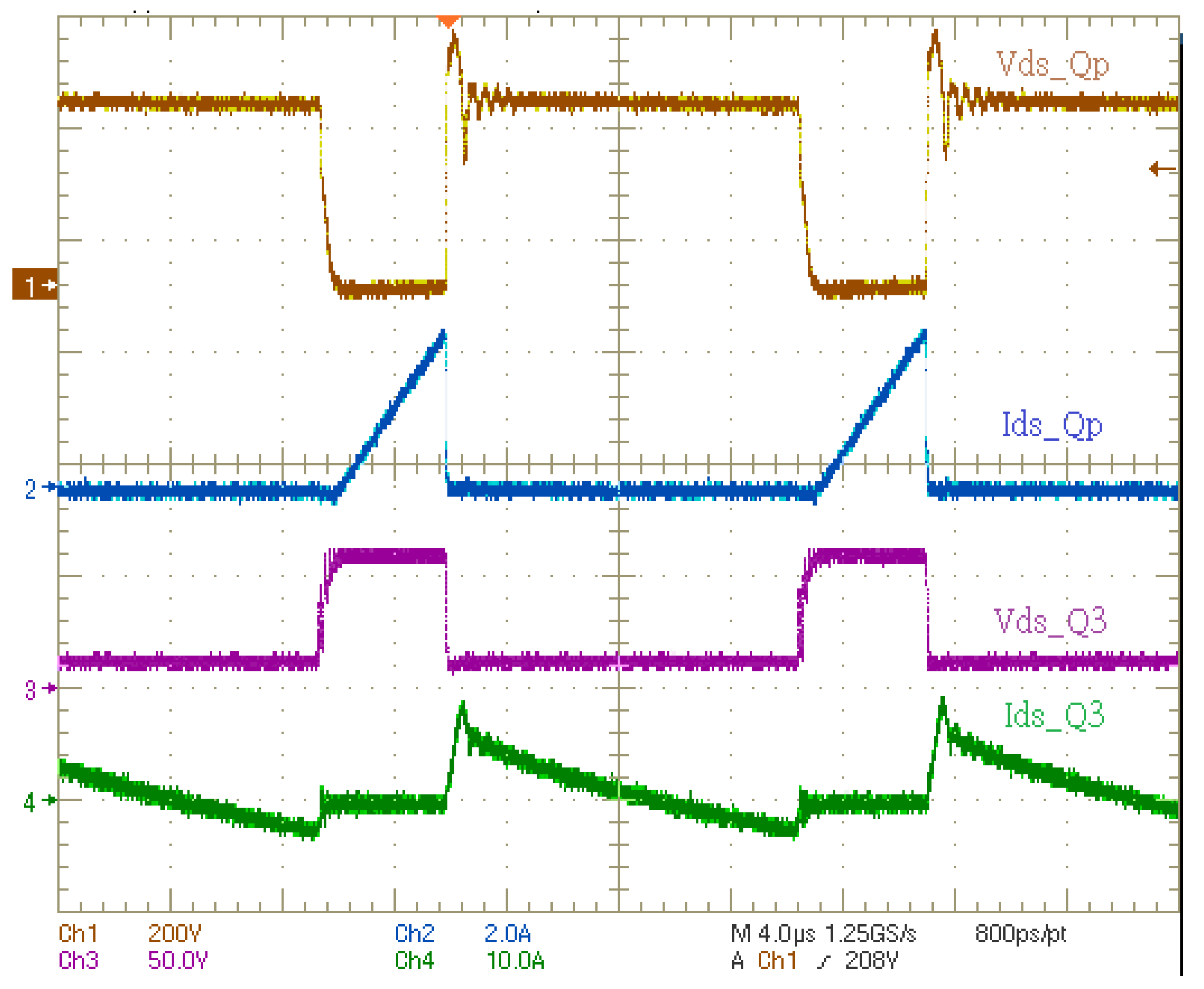
Figure 10 shows the waveforms of the main switch (Q
p) on the primary side and synchronous switch (Q
3) and the current (I
ds_Q3) on the secondary side. It indicates that the voltage stresses of the main switch and the synchronous switch are complementary. In the synchronous switch on period, the energy on the winding is released in the form of current.
For 24 V (R3), 12 V (R2) are in no load, 5 V (R1) is in heavy load condition. This is assuming the excitation energy of the primary side is completely transferred to the secondary side. In other words, the input energy of the primary side is equal to the output energy of the secondary side, which means Wp = 1/2LmIp2 + 1/2LιIι2 (the energy of magnetizing inductance + leakage inductance) = 1/2L1IN12 + 1/2L2IN22 + 1/2L3IN32 (the energy of winding 1 + 2 + 3). It would make the primary side excitation energy not only meet the energy demand of winding 1, but also the winding 2, 3 will consume the energy transferred from the primary side. Even if winding 2 and winding 3 are under no load conditions, winding 1 will be regulated to a specific voltage since it is a feedback winding. In fact, the loop impedance of winding 1 will cause a voltage drop due to a large current, which will make the voltage of winding 1 still slightly insufficient. Thus, it needs the feedback to the primary side to make the ON duty of Qp larger to satisfy the sufficient energy demand of winding 1 + 2 + 3.
Figure 11 shows the waveforms of the above cases. In the first period, the synchronous switches Q
1, Q
2, Q
3 are turned ON, the current of I
N3, I
N2 flows out from the winding to supply capacitors (C
3, C
2) and loads (R
3, R
2). At the second period, because R
3, R
2 are in no load, the remaining energy of the current turns into a negative direction and flows into the winding, and then is consumed by the heavy load winding (R
1). No matter in the first or second period, the output current (I
N1) is positive and flows out the winding for charging capacitor (C
1) and load (R
1), and no negative current flows into the winding.
Another case for 5 V (R1), 12 V (R2) are in no load, 24 V (R3) is in heavy load condition. It can also be understood that the loop impedance of the N3 winding (24 V) presents low impedance, and most of the energy transferred from the primary side passes through the N3 winding (due to the large current flowing through the low impedance loop). The current flow through the loop impedance of N1 and N2 is relatively small. In traditional multi-output winding, the voltage spike is generated by the leakage inductance and will be accumulated over time, thereby resulting in over-voltage at the output terminal. However, in the proposed design, the peak voltage energy is generated by the leakage inductance not only being consumed by R1 and R2, due to the continuous conduction of Q1, Q2, Q3, but also the remaining energy can pass through each other and release the energy.
Figure 12 shows the waveforms of the above cases. When the synchronous switches Q
1, Q
2, Q
3 are turned ON. The current of I
N1, I
N3 flows out from the winding to supply capacitors and loads. After the demands of R
1, C
1, R
2, C
2 are satisfied, the current continues to be released to 24 V (R
3) winding due to the stacked series structure. Only a small amount of energy of I
N2 is released to R
1 through the path of I
N1.
The case for 5 V (R
1), 24 V (R
3) are in no load, 12 V (R
2) is in heavy load condition, as shown in
Figure 13. When the synchronous switches Q
1, Q
2, Q
3 are turned ON first, the current of I
N3 flows out from the winding to supply C
3 and R
3. In the second period, because R
3 is in no load the remaining energy of current (I
N3) becomes negative current and flows into the winding, and then is consumed by the heavy load winding (R
2).
In addition, from the previous description, the excitation energy of the primary side (including leakage inductance energy) will not only meet the energy demand of winding 1. Even if winding 1 is in no load, the feedback to the primary side makes the primary side excitation energy does not store too much, but the secondary winding 2 depletes energy. Because winding 2 is in heavy load, the energy is exhausted quickly, although for winding 1 under no load, the energy transferred is still insufficient. Therefore, it will be fed back to the primary side to increase the ON duty of Qp to deliver enough energy for satisfying the winding 1 + 2 + 3.
When all windings are rated to load condition, and the load current of one winding is suddenly turned OFF. The waveforms of voltage and current are shown in
Figure 14a–c. It can be seen that even if the load current changes drastically, the voltage of all winding is not greatly affected.
Table 2 and
Table 3 summarize the steady state of each output voltage after the load current changes. The H means the winding under heavy load, and the L means the winding under no load. The regulation is from (MIN − TYP)/TYP × 100% and (MAX − TYP)/TYP × 100%; where MIN means minimum, MAX means maximum, and TYP means typical. It shows that the proposed design has good cross-regulation, even if the load current changes, the output voltage remains within a certain range.
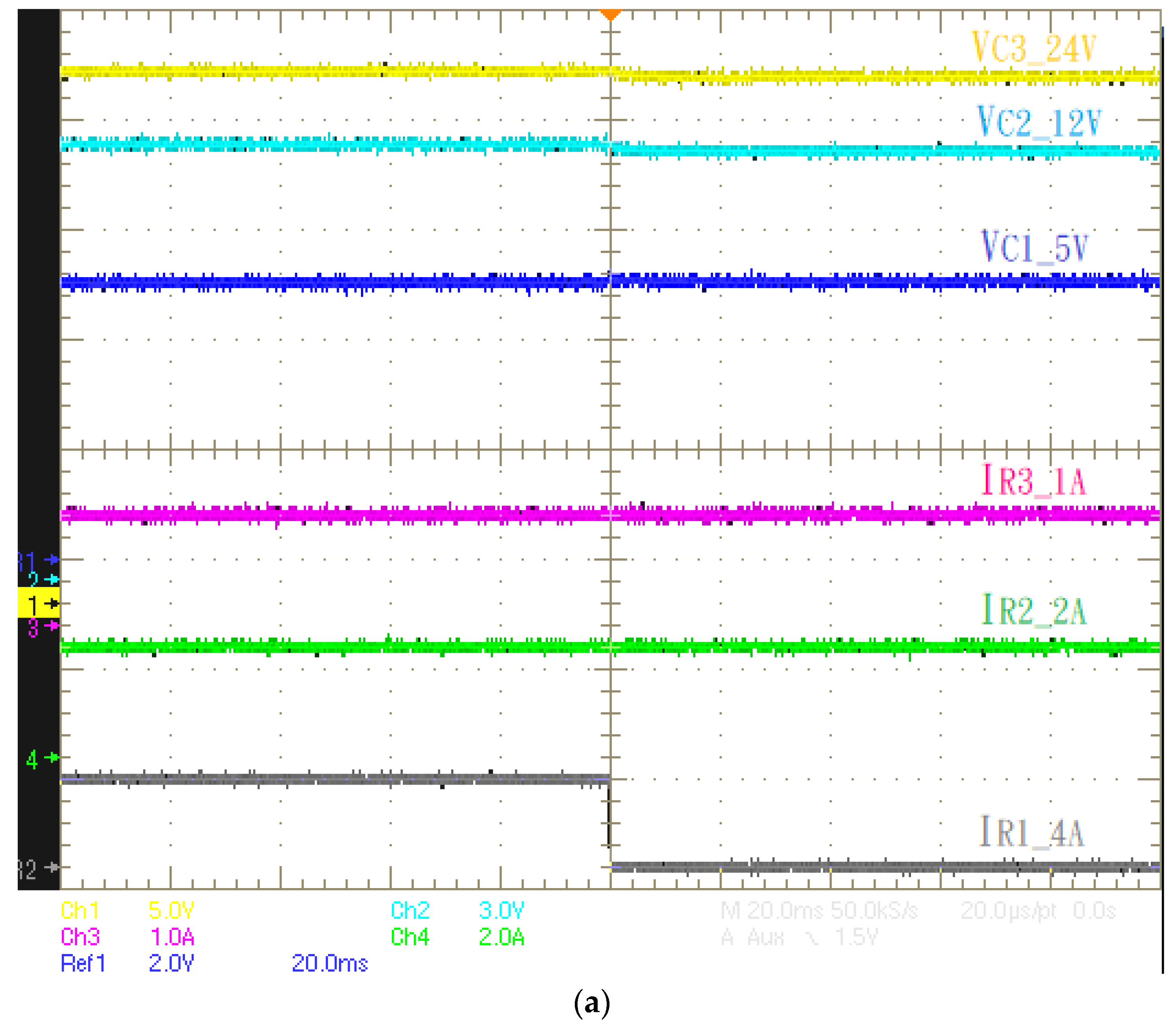
Table 4 and
Table 5 shows the voltage, current, power, efficiency data of the proposed converter in the full load range condition. The efficiency remains at a good level within the full load range.
Figure 15 shows the efficiency of the proposed three-output flyback converter from 10% to 100% load. Owing to the transformer contains air gap, the flyback converter’s typical efficiency is about 85%. The efficiency of the proposed converter is around 80~87%. The efficiency achieves the typical level. Furthermore, we built a typical flyback converter with the same specification, which is 5 V/4 A, 12 V/2 A, 24 V/1 A, and its output adopts the Schottky diode instead of synchronous rectification. From
Figure 15, the efficiency of the Schottky diode solution is much lower. But the proposed converter in full load range, the efficiency is maintained above a certain level. The efficiency values at 110 Vac increase first and then drop above 75% because the proposed converter is a single stage AC/DC flyback converter without PFC (power factor correction) stage. It operates in quasi-resonant mode, which means the frequency will change according to the load variation. When in heavy load at 110 Vac input, the switching frequency will decrease due to a long turn-on time, and the conduction loss becomes larger, so the efficiency is reduced. However, due to 220 Vac is a higher voltage. The frequency does not change much under heavy load, so the efficiency will not decrease.
Summarizing the advantages of the proposed converter, compared with reference [
6], the proposed converter does not require pre-load, so there is no additional loss. Reference [
7] needs a magamp post regulator. Reference [
8] needs extra turns wound around the outer leg of the core. Reference [
9] needs to design a clamp circuit. Reference [
10] needs to design small leakage inductance and PI controller. For reference [
11] it is necessary to develop an RCD snubber to absorb the energy of leakage inductance. References [
12,
13,
14,
15,
17,
18,
19] require an expensive controller to implement. References [
16,
21] require a transformer for each output. Reference [
20] requires two stages PFC + DC/DC. Most articles only use a DC/DC converter to discuss the cross-regulation issue of multiple outputs. However, they need to add an additional AC/DC stage for practical application. The proposed converter is a single stage AC/DC converter, and as can be seen from
Table 2 and
Table 3 it shows the cross-regulation can be effectively improved.


