1. Introduction
In modern computer architectures, the main memory for hardware acceleration is dynamic random-access memory (DRAM), which is advantaged by high density and low cost. Expanding data volumes have increased the number of parameters required in neural network models, the complexity of the calculation process, and accordingly the storage bandwidth of the system. Meanwhile, the capacity of DRAM remains limited, and from an architectural perspective, the utilization rate of DRAN is related to its access patterns. DRAM contains a multi-level matrix array of memory cells, usually with multiple banks. The two-dimensional matrices are organized into rows and columns. When data access different rows in the same bank of a DRAM, the previously accessed row must be precharged and the target access row must be activated. This operation, called row conflict or page conflict, requires a large number of cycles. Frequent row conflicts significantly reduce the memory performance and utilization, possibly causing serious latency and additional energy overheads. Therefore, minimizing the number of row conflicts is an important goal of memory system optimization.
At present, memory performance is usually optimized through memory address mapping [
1,
2,
3,
4], memory access scheduling strategies [
5,
6,
7], rearrangement of access data [
8,
9], and other methods that reduce the row conflicts. Although these technologies improve the system performance to a certain extent, they cannot effectively handle multiple memory access patterns for specific applications, because the memory access pattern is dynamically generated by the processor at runtime, and depends on the memory access characteristics of the application. Therefore, pre-designed memory optimization techniques perform poorly on applications that do not use the existing memory access patterns, and may cause severe performance loss.
Processor architecture design has benefited from the rapid development of neural networks, which allow architectures for specialized application domains [
10,
11,
12]. At present, many dedicated accelerator architectures have been designed, typically for neural network accelerators [
13,
14,
15]. However, the calculation method of a neural network impedes the performance of these architectures on central processing units, and GPUs are limited by the power consumption and area of the application platform. Field programmable gate array (FPGA) accelerators have attracted attention for their flexibility and energy efficiency, but in practical applications, there are two major problems with manually designed and optimized FPGA hardware accelerators. The first problem is the limited computing resources of the FPGA platform. Second is the large number of calculations and complex memory access patterns of the neural network of an accelerator, which overburden the memory system. To improve the performance of FPGA accelerator systems, we must optimize their memory access performance using a dedicated memory controller.
In this work, we propose a memory controller called NNAMC, and apply it to a convolutional neural network (CNN) accelerator. NNAMC operates at the whole hardware level to improve the memory system performance. During execution, it divides the memory banks and applies different address mapping schemes to different banks, thus isolating the different access stream patterns. After analyzing the memory access patterns of the address streams, NNAMC stores their different patterns in specific banks to optimize the performance requirements. The most difficult procedure is accurately identifying and analyzing the access data stream and the most suitable address mapping scheme for the memory access stream. In NNAMC, this critical problem is solved using a bank partitioning model (BPM). The memory access address sequence is completed by the data prediction unit of the previous item, and designs the optimal address mapping scheme in the partitioned bank.
The main contributions of this paper are summarized below.
The NNAMC design is based on an FPGA hardware development system, which is a memory controller dedicated to neural network accelerators, and is implemented in Very High speed integrated circuit hardware Description Language (VHDL) without excessive software operations.
A Steam Access Prediction Unit (SAPU) and a Bank Partitioning Model (BPM) were designed for NNAMC. The system performance is improved through professional prediction and classification of the memory access streams and the optimization of DRAM address mapping.
The performances of NNAMC and previous address mapping schemes were compared in typical test cases. The NNAMC outperformed the previous designs, and strongly adapted to different network parameters.
The remainder of this article is organized as follows.
Section 2 presents the background of DRAM, and
Section 3 discusses related work.
Section 4 describes the motivation of the proposed design.
Section 5 proposes the NNAMC design scheme, and
Section 6 presents the setup and results of the experiments. The article concludes with
Section 7.
2. Background
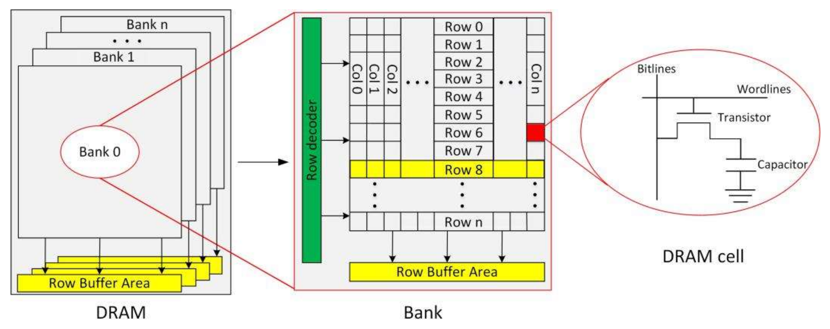
As shown in
Figure 1, a DRAM device is composed of multiple two-dimensional arrays of memory cells. Each two-dimensional array (called a bank) is composed of storage capacitors and transistors. The data are stored in the storage capacitors. Each DRAM cell is connected with a wordline and a bitline. In the vertical direction, the cells are connected to a row buffer area through the shared bitline, and in the horizontal direction, they are connected to the row decoder through the shared wordline. When data access the DRAM, the bank, row, and column IDs of the target address determine the specific DRAM location of the address, and the specific cell can be accessed by activating the specific bitline and wordline. The two-dimensional array structure of DRAM not only achieves efficient wiring, but also improves the operating speed and reduces the system’s power consumption.
Each bank in DRAM has a row buffer area connected by a bitlines. When accessing DRAM data, the row buffer can be used as a cache for storing all data in the row accessed by the previous address. If two consecutive memory accesses refer to the same row of the same bank in the DRAM, the access latency will be low. In this scenario, only the target cell in the row buffer corresponding to the column ID of the current address must be located. This operation is called a row buffer hit (or page hit). If the target rows of two consecutive accesses are different rows in the same bank, a row conflict occurs, meaning that the memory continuously accesses different rows in the same bank. In this scenario, the current row must be closed by issuing a precharge command, and the row to be accessed by the next address must be opened by issuing an active command. However, as banks are arranged in parallel, two adjacent instructions in different rows of different banks will avoid row conflicts. Row conflicts usually increase the latency and energy consumption. The latency of row conflict access is 3.5 times that of row buffer hit. Therefore, increasing the row buffer hit ratio will greatly improve the memory performance of DRAM.
The main page policies of modern DRAM are the open-page policy (OPP) and the close-page policy (CPP) [
16,
17]. As an example, the access latency of DDR3-1600 memory in OPP and CPP modes are shown in
Table 1.
OPP is widely used in memory systems with few computer processors. In contrast, CPP supports access to random memory locations and memory request modes with low access localities. CPP is usually used in the memory systems of many processor systems, multi-processor systems, or dedicated embedded systems. Depending on the system, different row buffer management strategies can optimize the performance or minimize the power consumption of the memory system.
3. Related Work
3.1. Address Mapping
Address mapping converts a memory address to the corresponding physical storage unit based on the arrangement of bank ID, row ID, and column ID. Address mapping is among the most commonly used methods for reducing the row conflict of the system.
Figure 2 shows several commonly used address mapping schemes proposed by previous researchers. Panels (a) and (b) show the bank–row–column (BRC) [
18] and row–bank–column (RBC) [
18] schemes, which exchange an upper bank bit in the address with a low row bit. Xilinx proposed the most advanced memory interface generator (MIG) [
18] IP core using these mapping schemes. In addition to the BRC and RBC mapping schemes, MIG provides a test address mapping scheme. The complex memory controller supports permutation-based page interleaving (PBPI) [
1], as shown in
Figure 2c. The new bank bit is obtained through an XOR operation of the address’s bank bit and a low row bit. The parallelism of the bank ensures the maximum DRAM utilization, and the lowest three row bits are usually selected for XOR operation. Bit reversal [
3] (
Figure 2d) reverses the bits corresponding to the bank and row bits in the original physical address. Minimalist open-page (MinOP) [
4] (
Figure 2e) partitions the column positions, placing the least significant bits after the bank bits, and the most significant bits before the row bits. The low-order row bits are then XORed with the bank bits to generate new bank bits. The authors of [
2] proposed a binary invertible matrix (BIM) for GPU mapping (
Figure 2f), which represents memory remapping operations. The BIM composes all address mapping schemes through AND and XOR operations, and exploits its reversibility property to ensure that all possible correspondences are considered. DReAM [
19] analyzed the switching rate at runtime and changed the address mapping on the fly, but this scheme incurs a large overhead. Whereas current memory controllers convert physical addresses using a single address mapping scheme, which is not very flexible, our proposal scheme eliminates this concern.
3.2. Special Memory Controller
Special memory controllers effectively improve the memory performance of DRAM. The memory controller CONCEPT [
20] exploits the unique performance of RRAM to improve the performance and energy efficiency and can also calculate processing in memory. The authors of [
21] proposed a self-optimized memory controller design that observes the system state with reinforcement learning, and evaluates the long-term performance impact of each operation. The authors of [
22] proposed an access prediction technology for multimedia applications. Their system tracks the memory data access information of the executed instructions, and dynamically predicts different access patterns. PARDIS [
23] is a programmable memory controller based on a standard reduced instruction set computer. The address mapping of a specific application program is realized through offline analysis, which improves the memory performance. In [
24] the authors proposed a specific access pattern that optimizes the bandwidth of fast Fourier transform-based applications. The authors of [
25] proposed a prefetch architecture with two-dimensional access for image processing. However, these controllers cannot be used in software-less systems such as ASIC or FPGAs.
3.3. Bank Partitioning
The row conflicts between threads can be reduced by partitioning the banks between memory applications. The authors of [
26] proposed a software method that effectively eliminates the interferences without hardware modification. Page coloring is a BPM that allocates specific threads and implements a thread cluster through the memory controller. This technique passively schedules the memory requests. Dynamic bank partitioning integrated with thread cluster memory scheduling [
27] compensates for the low parallelism caused by bank partitioning, and estimates the number of banks to guide the bank partitions. This method improves the throughput and fairness of the system. A new software and hardware cooperative BPM for DRAMs combines page coloring and BPBI mapping and reduces the inter-thread interference [
28,
29]. The authors of [
30] proposed a DRAM memory aware memory allocator with a page-based virtual memory system, which allocates the memory pages of each application to a specific memory. Their allocator avoids sharing the memory library between the cores, thereby eliminating the need for special hardware stand by.
4. Motivation
This section explains the motivation of our study. To this end, we demonstrate a CNN accelerator on image mapping. The accelerator stores the image data in DRAM, and reads the pixel data using a CNN-like computing operation. The reading method maps the image pixels to the memory system by address mapping. We call this process an Address and Pixel Transaction (APT).
4.1. Address and Pixel Transaction
APT is a local unit that maps image pixels to DRAM by address mapping. As an example, we consider sequential access during a CNN calculation.
Figure 3a is the sequential access map. The address increases along the horizontal direction of the image, scan the next line when the horizontal scan is completed. ImgW and ImgH are the width and height of the image, respectively, in units of pixels, and the initial address is that of the allocated memory space. During the sequential access, the address of the image coordinates (A, B) is given by:
Suppose that the image size is 60 × 80, the initial address is 0 × 0000, and each pixel requires 16 bits. The APT of coordinate (79, 59) is Address = 0 + [(59 − 1) × 80 + 79] × 16 = 75,504 bits, and the hexadecimal number of the converted memory standard address is 0 × 126F0.
Figure 3b shows the memory mapping of this address. The physical address 0 × 126F0 is mapped following the BRC scheme. The APT corresponding to this pixel is in the zeroth and first banks, and the DRAM cell in the 49th row and 752th column performs the storage [
31].
Image access by DRAM uses various access patterns. In our image convolution computation, we applied 2D access. The size of the convolution kernel was 3 × 3, the stride was 1, and the 2D access was based on APT. The results are shown in
Figure 3c. When accessing a DRAM cell, if the accessed data are not in the row buffer of the current bank, the current row must be precharged, the target row is reactivated, and a read/write command is issued. Such row conflict operations are energy and time consuming.
Figure 3c shows the address sequence of accessing this segment. Among the 11 accessed address sequences are four row conflicts, which can seriously harm the memory system. During a row conflict, other operations cannot be performed in the same bank. The memory access patterns for image memory access operations are many and varied. Our NNAMC exploits this variability to optimize the DRAM performance and reduce the number of row conflicts.
4.2. Motivation—Memory Access of CNN Accelerator
The memory performance is related to the memory access pattern of an application. Arithmetic operations are complicated processes for accelerators and demand a burdensomely high memory bandwidth from the memory system. We consider the CNN accelerator because the typical memory access patterns in CNN calculations cover more than 95% of all memory access types of image processing [
32].
Figure 4 is an example of a CNN accelerator. First, the accelerator obtains the feature maps and weights on the host side and stores them in the memory system. Second, the FPGA computing unit extracts the feature map and weights from the memory for calculation. Repeating this step, a feature map is extracted and calculated for each operation, and is stored in the memory system. Finally, the system calculation results are transmitted back to the host.
Owing to the characteristics of CNN convolution computation, row conflicts in the memory system are common occurrences during accelerator access. When the PE performs the convolution calculation, the accelerator accesses the memory data two-dimensionally (see
Figure 3c). A series of visits can cause serious row conflicts. Among the 11 accessed address sequences, the rows were precharged and reactivated four times, increased access latency by 2.4 times. The calculation formula of the memory access delay multiples (Ratio of the current system running time to the system full row buffer hit running time) is as follows:
The access patterns of CNN calculations include (but are not limited to) sequences, strides, two-dimensional patterns, and random accesses. Input feature maps and weights of different sizes will also seriously affect the memory access characteristics of the system. Using the characteristics of different access maps, NNAMC designs a dedicated memory controller for neural network accelerators.
5. Proposed Architecture—NNAMC
5.1. Overview
NNAMC is a novel technology that analyzes the memory access patterns of a neural network accelerator during its operation. By allocating the optimal address mapping scheme, NNAMC reduces the number of row conflicts and improves the memory performance. The proposed NNAMC (see
Figure 5) realizes a novel structure for hardware memory controllers. Its four design components are Address Access Behavior Monitoring (AABM), SAPU, bank retag, and a BPM. The memory controller is applicable to most neural network accelerators and is compatible with the workflow in
Figure 4.
The AABM monitors the memory access requests sent by the accelerator to the memory controller. Because AABM applies FIFO strategy, the memory controller quickly identifies the information of each memory access request. This strategy maximally simplifies the cache preprocessing operation of the address stream, and reduces the expense of tracking and monitoring the address stream in DRAM.
The SAPU stores and analyzes the input address stream and the parameters of the neural network. This component divides the memory request into four subtypes with different access patterns: sequential, stride, 2D, and random. The access type is determined by a fine-grained CNN, which effectively guides the subsequent scheduling of the memory system, and the BPM is maximized. The implementation of SAPU is detailed in
Section 5.2.
The BPM includes bank retag and bank partitioning. The bank retag rearranges the bank of the address stream. The bank partition imposes strict requirements on the setting of the address mapping scheme in that bank. Therefore, different patterns of the address streams entering the target bank can be assured only by rearranging the banks. Under the optimized address mapping scheme for the target bank, the bank partitioning specifically maps each access stream to maximize the performance of the bank accessed by the access stream.
These four components comprise the NNAMC architecture. By improving the memory controller hardware, we can improve the memory performance while fully utilizing the storage bandwidth. Once the access types of the continuous access requests have been forecasted and scheduled by SAPU, the row buffer hit ratio is maximized by bank partitioning model operations.
5.2. Accelerator Access Prediction
The SAPU discriminates the address stream type in the NNAMC architecture. The SAPU is composed of four functional units: parameter reference table (PRT), parameter computing unit (PCU), comparative decision logic (CDL), and arbitration logic (AL). As shown in
Figure 6, the SAPU monitors all access streams and neural network parameter information, and updates the access history in the PRT. Besides saving the historical information, the PRT reorganizes the internal threshold data, and enters the number of decisions into the CDL. The PCU calculates the various parameters of the PRT and their thresholds M, and generates a difference address table. The CDL calculates and compares the RPT and PCU input values and generates binary logic numbers, which are input to the AL for judgment and decision-making. This subsection introduces the structure and function of these four units, which collectively determine the access pattern of the stream.
5.2.1. Parameter Reference Table (PRT)
The PRT stores the address streams, network parameters, and system operation results in internal entry tables. When the accelerator accesses the memory system, the image length and window size in the entry tables are updated in response to the storage requests from the accelerator. The size of the entry table stored in the address stream depends on the size of the physical address. In this paper, the entry table was configured to store 27 bits physical addresses, and the entry table storage address stream was divided into two cases. When the PRT lacked the access instruction addresses and network parameters (first case), a new entry table was created. When the instruction address in the entry table contained valid entries (second case), the entry table was incremented until the entry reached its upper limit, and was then passed to the PCU. The neural network parameter storage part mainly stored the basic information (image length and window size). As the basic information was more-or-less fixed, this part of the item table was generally constant. The result of the system operation was stored in the AL. Each entry table of the storage information was stored as a 3 bits binary number.
5.2.2. Parameter Computing Unit (PCU)
The PCU obtains the numerical value in the PRT entry table, and calculates the SAPU reference value. The PCU comprises two parts: an address difference storage unit and a parameter threshold calculation unit. The address difference storage unit calculates the difference Dif_addr between the previous and current addresses in the PRT entry table. The previous and current addresses are 27 bits unsigned addresses and Dif_addr is a signed addresses calculated as:
Each calculation result Dif_addr is stored in the signed address difference memory Dif_ram. This memory is composed of multiple address storage units, and its depth depends on the local parameter kernel of the neural network, which is found in the PRT entry table. The parameter kernel of the benchmark in this paper is 11, implying that the design conforms to the hardware design rules and introduces no large timing latency to the system. The counter controls the full threshold of Dif_ram. When the value stored in Dif_ram reaches kernel-1, the enable ram_en of the Dif_ram is closed, and the internal Dif_ram is full.
The parameter threshold calculation unit mainly calculates the network parameters and sets the reference threshold of the CDL. The internal neural network parameters of the system are integrated to obtain the new image width and kernel. The calculations are given by Equations (4) and (5), respectively:
The reference thresholds M and N of comparator A and the counter in the CDL are respectively computed as:
5.2.3. Comparative Decision Logic (CDL)
The CDL obtains the value in each storage block of Dif_ram, and generates the reference value. The CDL comprises a comparator, a shift register, an AND gate, and a counter (
Figure 6). Decision-making is performed by the following steps:
- (1)
All values in Dif_ram are transferred into Com C. If all values are equal, the output 1 is sent to the S1 end of the AL;
- (2)
The value in the last block of the Dif_ram storage unit (the kernel-1 block) is transferred to the shift register. If the upper 8 bits of the data in the shift register are F, the shift register outputs 1.
- (3)
The PCU output reference threshold M, and the data of Dif_ram (kernel-kernel_size-1 … kernel_size) value of 1 storage unit, are transferred to Com A. If the data in Com A are equal, then Com A outputs 1.
- (4)
Com B judges whether the values of the other storage units except the first kernel-kernel_size-1 … kernel_size-1 storage unit equal the value in the kernel-1 storage unit. If the answer is yes, then Com B outputs 1.
- (5)
The outputs of Com A, B, and the shift register are computed by AND logic and the result is input to the S0 terminal of the AL.
- (6)
If all Dif_ram values in the count memory of Counter are the product of Image_width × Pixel, and the number of Image_width × Pixel is N, then Counter outputs 1. This result is input to the S2 terminal of the AL.
5.2.4. Arbitration Logic (AL)
The AL generates an address access memory pattern based on CDL signals. The AL constitutes a single decoder whose input terminals S0, S1, and S2 provide binary-number combinations on the four output results (Y0-Y3), corresponding to 100, 010, and 001. The AL output is stored in the entry table of the PRT, and is used as the memory access pattern of the current address stream.
In the example of
Figure 7, the CNN accelerator dynamically predicts the memory access to a 960 × 1280 image using the 2D access pattern. The figure shows the network details when a 3 × 3 window slides over the image and the first pixel of the window is stored at the physical address 0003D3B8. As the network kernel is 9, the nine instructions are recorded and changed in turn. The nine differences are stored in Dif_ram. Among these values, the difference stored in Dif_ram [2] and Dif_ram [5] (000027F0) is equal to M (10224D) output by the PCU, the difference stored in Dif_ram [8] is FFFFAFF8 (<0), and the remaining entries Dif_ram [0], Dif_ram [1], Dif_ram [3], Dif_ram [4], Dif_ram [6], and Dif_ram [7] are all equal. The output terminal S0 of the AND gate is 1, the output terminals S1 and S2 are 0, and the AL output is 100, denoting that the memory access address stream follows the 2D memory access pattern.
5.3. Bank Partitioning Model
Based on the observations in
Section 3.2, we propose a BPM that considers the address mapping requirements of multiple patterns of access streams to reduce the number of row-buffer conflicts.
Figure 8 shows the basic principle of bank partitioning. Considering the characteristics of CNNs, the basic memory-access patterns of the BPM are divided into sequential, 2D, stride, and random (Memory access patterns detailed in
Section 6.1).
Figure 8a shows the traditional memory access pattern. All DRAM banks adopt a unique address mapping scheme and sample the same address-mapping scheme for all memory access streams. In previous work, the memory access performance was improved by modifying and optimizing the address-mapping scheme, but when the accelerator simultaneously runs multiple memory access streams, row conflicts and memory access latency can reduce the system performance. Some memory access streams require specific address mapping. For example, when the memory access stream of stride with different image sizes and pixel size pairs are accessed using the RBC scheme. In such cases, the previous methods will cause severe extremes and instability that greatly reduce the memory access performance.
Figure 8b shows the bank partitioning scheme adopted in NNAMC. After partitioning the DRAM banks, RBC address mapping and BPBI address mapping were applied to the low banks (LBS) and high banks (HBS), respectively. The scheme was implemented in two steps: (1) Analyzing the memory access behavior of the SAPU address stream and applying bank retag to the address stream; and (2) forming decisions on the bank-level memory access.
The task of bank retag is rearranging the banks. Bank partitioning is difficult, because it must ensure that the memory streams enter the target bank as required. The LBS and HBS in the above division each occupied four banks. The bank retag operation is shown in
Figure 9. Based on the hardware design, we cached each memory access stream using a FIFO operation. The memory bank of the address mapping scheme adopted by NNAMC is set in the 10th to the 12th bits. The 12th bit of each address of the sequence and the 2D address streams were ANDed with 0, meaning that all sequences and 2D address streams adopted the RBC address mapping scheme. For the stride memory access pattern, the 12th bit of each address and 1 were subjected to the OR operation, meaning that all address streams of the stride adopted BPBI address mapping, thus realizing the bank retag.
Bank-level access decisions are made for two reasons. First, we can isolate memory access patterns with large performance differences, fully utilize the memory space locations, and reduce the interference between memory access streams. LBS uses RBC address mapping and HBS uses BPBI address mapping.
Figure 9 explains that bank retag is used to receive the sequential and 2D access patterns. HBS is used to receive the stride access pattern. Our proposed NNAMC adopts a hybrid address mapping schemes, which is the result of 225 experimental selections for various CNN parameters. The experimental results show that the row buffer hit ratio of sequential access pattern can reach 72.7–99.99% (90.52% on average). The row buffer hit ratio of 2D access pattern can reach 74.22–98.95% (87.02% on average). But the row buffer hit ratio of the stride access pattern is only 0–100% (51.18% on average). Because of the huge fluctuation of the row buffer hit ratio of stride access (the floating range spans 0–100%), we choose the BPBI address mapping that is optimal for stride access for HBS. BPBI row buffer hit ratio can reach 87.5% for stride access scheme. We choose the RBC address mapping for sequential and 2D access patterns. Random access patterns, most of which constitute image noise, are unstable and do not require specific address mapping schemes. Second, we can increase the accelerator’s sensitivity to memory access streams and fully exploit the parallelism of the banks, thereby increasing the system throughput. Here we constructed up to eight banks from DDR3-1600 memory modules.
In bank retag, the rearranged memory-access address may be the same as the previous or subsequent memory-access address, which leads to the loss or conflict of system data. In bank retag simulations, the probability of obtaining identical addresses after bank retag rearrangement was found to be very low. Among the total number of system addresses, the low probability of identical addresses is acceptable and will not affect the system process. Moreover, the NNAMC was designed for CNN hardware accelerators. The probability of data loss minimally impacts on neural networks [
33]. In fact, the probability of noise in CNN images is much higher than the probability of data loss by bank retag.
6. Experimental
6.1. Experimental Setup
6.1.1. Benchmark Selection
To demonstrate that NNAMC can flexibly adapt to CNN hardware accelerators, we tested the performance of NNAMC on four typical CNN accelerator memory access patterns: sequential, 2D, stride, and random. According to Jang et al. [
32], these memory access patterns cover more than 95% of CNN application scenarios. For each memory access pattern, NNAMC was tested in a representative CNN operation scenario as described below.
Sequence: As shown in
Figure 3a, the accelerator linearly accesses the memory on the chip, and a memory with sufficient space can store a large amount of output data. In this test, the convolution calculation result of the feature map in CNN was accessed and arranged in a sequential manner, and all data were cached on the chip by the accelerator during the calculation process.
2D: In this test, the convolution computation of CNN was a typical 2D access pattern. The convolution kernel scanned the image using a 2D window. 2D memory access is the most important memory access pattern in CNNs, accounts for most of all CNN operations.
Stride: In this test, the CNN adopted a cascaded fully connected layer as the system classifier. The stride access pattern can test matrix–vector multiplications, which are periodically performed by hardware accelerators. The stride access pattern is used not only in CNN calculations, but also in image processing applications.
Random: Losses of image pixels in the CNN calculation or losses of access data in the accelerator operation were given random addresses in the original address sequence.
In the sequence and stride access tests, the selected images were sized 600 × 800, 768 × 1024, and 960 × 1280, and the pixel sizes were 8, 16, and 32 bit. For the 2D access pattern, we chose images and pixel sizes giving the same resolution as the sequence and stride tests. For the kernel part, we selected three typical CNN kernels: 3 × 3, 7 × 7d, and 11 × 11. References [
19,
34] also provide similar but different application benchmarks, which does not affect the experimental results. The runtimes of the benchmarks based on the above selections are shown in
Figure 10. All runtimes were measured on an Intel core i5-6500 (4-core) system.
To show the advantages of NNAMC dedicated to CNN hardware accelerators, several existing address mapping schemes were selected for a performance comparison: BRC [
18], RBC [
18], BPBI [
1], Bit reversal [
3], and MinOP [
4].
6.1.2. Experimental Platform
The whole system was implemented on a Xilinx VC707 FPGA. The FPGA development board includes a Virtex-7 VX485T FPGA chip and a 1 GB Micron DDR3 DRAM. Each physical address contains 27 bits: 3 bits bank coordinates, 14 bits row coordinates, and 10 bits column coordinates. The NNAMC design was based on a Xilinx MIG IP Core and implemented in Verilog HDL. To clarify the performance improvements after optimizing the address mapping scheme, we closed the memory access scheduling, page policy optimization, and all other optimization techniques.
6.2. Results
6.2.1. Experimental Results
The performance of NNAMC was compared with those of previously proposed address mapping schemes on the same benchmarks of the dedicated CNN accelerator. The two most important indicators of a memory system (row buffer hit ratio and access latency) were selected as performance measures. First of all, the operands of various memory access patterns in the benchmark are verified by equal processing. The experimental results are shown in
Table 2. In the 27 test cases, NNAMC was compared with the other address mappings (BRC, RBC, BPBI, Bit reversal and MinOP), the row cache hit rate increased by 43%, 12.46%, 17.90%, 11.32%, 11.36%, respectively. The overall average row cache hit rate increased by 19.21%, proving the importance of the NNAMC prediction unit and the effectiveness of bank partition optimization. The address mapping scheme adopted by NNAMC assigned the bank to a mid-address bit, reflecting the strong stability of NNAMC; accordingly, the fluctuations in the row buffer hit ratio were not large.
In order to verify the ability of NNAMC to reduce system memory access latency, all address mapping strategies were tested on FPGA, and the memory access latency of each test example was reported in
Figure 11. As shown in the figure, NNAMC can indeed reduce the access latency of the system. Compared with other address mappings (BRC, RBC, BPBI, Bit reversal, and MinOP), the designed NNAMC reduces the access latency by 15.04 ns, 4.36 ns, 6.26 ns, 3.96 ns, and 3.97 ns, the overall average access latency was reduced by 33.03%, and the maximum access latency was reduced by 52.57%.
The main task of a CNN hardware accelerator is accelerating the convolutional layer of the CNN. The convolutional layer performs most of the total number of CNN operations. Accordingly, we increased the calculation operations of all benchmark convolutional layers, until the 2D access required for the convolution calculation reached the set value. The row buffer hit ratio results are shown in
Table 3, and the access latency is compared in
Figure 12. In all test cases, NNAMC achieved a higher row buffer hit ratio than the other address mappings. In this mode, our design NNAMC and other address mappings (BRC, RBC, BPBI, Bit reversal, and MinOP) row buffer hit ratio increased by 24.61%, 4.1%, 16.06%, 11.8%, 11.85%, the overall average row buffer hit ratio increased by 13.68%. The system access latency was reduced by 8.61 ns, 1.44 ns, 5.62 ns, 4.13 ns, 4.16 ns, the overall average access latency was reduced by 26.3%, and the maximum access latency was reduced by 37.68%.
The experimental study shows that the memory access performance access performance is affected by interference from multiple memory access patterns. It should be noted that the stride access pattern is that image pixels are stored by vertical mapping to the memory system, which has a huge impact on the memory access performance. In the actual CNN accelerator system, the stride access pattern is mainly used for the calculation of the fully connected layer, and the number of operands required is much lower than that of the convolution calculation, which can explain the experimental results in the above-mentioned specific configuration. In general, NNAMC can optimize the row buffer hit ratio and access latency at the same time by predicting the pattern of memory access stream and address mapping partition, thereby improving the system performance.
6.2.2. Hardware Resource Utilization
Table 4 gives the hardware resources utilized by the memory controller of NNAMC. The NNAMC was realized by modifying MIG, mainly, by modifying the address mapping scheme and SAPU in Verilog HDL. The system energy consumption was not only related to the row buffer hit ratio, but also related to the system voltage and frequency. A large number of precharge will cause a lot of energy consumption [
2]. The proposed NNAMC can increase the row buffer hit ratio by 13.68% on average. The system voltage is 1.8 V and the system frequency is 200 MHz.
As shown in
Table 4, NNAMC occupied few FPGA on-chip resources, leaving a large resource space for designing the CNN hardware accelerators. Especially, NNAMC consumed few FPGA on-chip storage resources BRAM and FPGA on-chip FFs. The NNAMC utilization of both logics was approximately 5% of the target FPGA device. Therefore, the area overhead of NNAMC was deemed appropriate. The proposed method was unaffected by the number of network parameters and size of the address flow, required no modification of other system components, and did not affect the design parameters of the other components.
6.2.3. Other Analysis
Finally, we confirmed the performance robustness of NNAMC to changing network parameters. This test was performed on differently sized images, image pixels, and convolution kernel sizes of the CNN model. Subsequently, we tested the memory access performance of NNAMC on the address sequences corresponding to different parameters. The image sizes were selected as 480 × 720, 600 × 800, 768 × 1024, 960 × 1280, and 1080 × 1920; the pixel sizes were selected as 4 bits, 8 bits, 16 bits, 32 bits, and 64 bits; the convolution kernel sizes were typically 2, 3, 5, 7, and 11. The test results are shown in
Figure 13. The average row buffer hit ratio of NNAMC in image sizes, pixel sizes, and convolution kernel sizes compared with other address maps increased by 16.17%, 19.96%, and 14.57%, respectively. Experimental results show that no matter how the image sizes, pixel sizes and convolution kernel sizes of the network parameters change, NNAMC can still reflect a high memory access performance.
7. Conclusions
In this work, we propose a memory controller called NNAMC. NNAMC uses SAPU to predict the memory access pattern of the CNN hardware accelerator, and uses the BPM to optimize the address mapping scheme. The experimental results show that NNAMC suitable for most of the memory access patterns of CNN hardware accelerators provides the optimal address mapping scheme, and the memory access performance is better than the address mapping scheme provided by the previous generation. We have also implemented NNAMC on the hardware system, which has a low on-chip resource occupancy rate and also leaves a lot of space for other accelerators. In addition, NNAMC has shown superior performance to mainstream neural networks and can adapt to various network parameters.
Author Contributions
Conceptualization, R.W. and G.S.; methodology, C.C. and C.L.; validation, C.L.; investigation, C.L.; resources, C.C.; writing—original draft preparation, C.L. and C.C.; writing—review and editing, R.W., C.L., C.C., G.S., and M.H.; visualization, R.W. and C.L.; supervision, C.C. and M.H.; project administration, R.W. and G.S. All authors have read and agreed to the published version of the manuscript.
Funding
This research was supported by the National Natural Science Foundation of China (Grant No. 92064006).
Conflicts of Interest
The authors declare no conflict of interest.
References
- Zhang, Z.; Zhu, Z.; Zhang, X. A permutation-based page interleaving scheme to reduce row-buffer conflicts and exploit data locality. In Proceedings of the 33rd Annual IEEE/ACM International Symposium on Microarchitecture (MICRO-33), Monterey, CA, USA, 10–13 December 2000; pp. 32–41. [Google Scholar]
- Liu, Y.; Zhao, X.; Jahre, M. Get out of the valley: Power-efficient address mapping for GPUs. In Proceedings of the 2018 ACM/IEEE 45th Annual International Symposium on Computer Architecture (ISCA), Los Angeles, CA, USA, 1–6 June 2018; pp. 166–179. [Google Scholar]
- Shao, J.; Davis, B.T. The bit-reversal SDRAM address mapping. In Proceedings of the Workshop on Software and Compilers for Embedded Systems, Dallas, TX, USA, 29 September–1 October 2005; pp. 62–71. [Google Scholar]
- Dimitris, K.; Jeffrey, S.; Lizy, K.J. Minimalist open-page: A DRAM pagemode scheduling policy for the many-core era. In Proceedings of the 2011 44th Annual IEEE/ACM International Symposium on Microarchitecture (MICRO), Porto Alegre, Brazil, 3–7 December 2011; pp. 24–35. [Google Scholar]
- Rixner, S.; Dally, W.; Kapasi, U.J. Memory access scheduling. In Proceedings of the 27th International Symposium on Computer Architecture, Vancouver, BC, Canada, 14 June 2000; pp. 128–138. [Google Scholar]
- Mutlu, O.; Moscibroda, T. Parallelism-aware batch scheduling: Enhancing both performance and fairness of shared DRAM systems. In Proceedings of the 2008 International Symposium on Computer Architecture, Beijing, China, 21–25 June 2008; pp. 63–74. [Google Scholar]
- Kim, Y.; Han, D.; Mutlu, O.; Harchol-Balter, M. ATLAS: A scalable and high-performance scheduling algorithm for multiple memory controllers. In Proceedings of the 2010 The Sixteenth International Symposium on High-Performance Computer Architecture (HPCA-16), Bangalore, India, 9–14 January 2010; pp. 1–12. [Google Scholar]
- Sudan, K.; Chatterjee, N.; Nellans, D.; Awasthi, M.; Balasubramonian, R.; Davis, A. Micro-pages: Increasing DRAM efficiency with locality aware data placement. In Proceedings of the 15th International Conference on Architectural Support for Programming Languages and Operating Systems, Pittsburgh, PA, USA, 13–17 March 2010; pp. 219–230. [Google Scholar]
- Dong, X.; Xie, Y.; Muralimanohar, N. Simple but effective heterogeneous main memory with On-Chip memory controller support. In Proceedings of the 2010 ACM/IEEE International Conference for High Performance Computing, Networking, Storage and Analysis, New Orleans, LA, USA, 13–19 November 2010; pp. 1–11. [Google Scholar]
- Guan, Y.J.; Yuan, Z.H.; Sun, G.Y.; Cong, J. FPGA-based accelerator for long short-term memory recurrent neural networks. In Proceedings of the 22nd Asia and South Pacific Design Automation Conference (ASP-DAC), Tokyo, Japan, 16–19 January 2017; pp. 629–634. [Google Scholar]
- Guan, Y.J.; Liang, H.; Xu, N.Y.; Wang, W.Q.; Shi, S.S.; Chen, X.; Sun, G.Y.; Zhang, W.; Cong, J. FP-DNN: An automated framework for mapping deep neural networks onto FPGAs with RTL-HLS hybrid templates. In Proceedings of the IEEE 25th Annual International Symposium on Field-Programmable Custom Computing Machines (FCCM 2017), Napa, CA, USA, 30 April–2 May 2017; pp. 152–159. [Google Scholar]
- Parashar, A.; Rhu, M.; Mukkara, A.; Puglielli, A.; Venkatesan, R.; Khailany, B.; Emer, J.; Keckler, S.W.; Dally, W.J. SCNN: An accelerator for compressed-sparse convolutional neural networks. In Proceedings of the 44th Annual International Symposium on Computer Architecture (ISCA), Toronto, ON, Canada, 24–28 June 2017; pp. 27–40. [Google Scholar]
- Zhang, P.; Li, G.; Sun, Y.; Guan, B.; Cong, J. Optimizing FPGA-based accelerator design for deep convolutional neural networks. In Proceedings of the 2015 ACM/SIGDA International Symposium on Field-Programmable Gate Arrays, Monterey, CA, USA, 22–24 February 2015; pp. 161–170. [Google Scholar]
- Zhang, M.; Li, L.P.; Wang, H.; Liu, Y.; Qin, H.B.; Zhao, W. Optimized Compression for Implementing Convolutional Neural Networks on FPGA. Electronics 2019, 8, 295. [Google Scholar] [CrossRef]
- Zhang, X.L.; Wei, X.; Sang, Q.B.; Chen, H.; Xie, Y.Z. An Efficient FPGA-Based Implementation for Quantized Remote Sensing Image Scene Classification Network. Electronics 2020, 9, 1344. [Google Scholar] [CrossRef]
- Alawneh, T.A.; Elhossini, A. A prefetch-aware memory system for data access patterns in multimedia applications. In Proceedings of the 15th ACM International Conference on Computing Frontiers, Ischia, Italy, 8–10 May 2018; pp. 78–87. [Google Scholar]
- Sun, H.; Chen, L.; Hao, X.R.; Liu, C.J.; Ni, M. An Energy-Efficient and Fast Scheme for Hybrid Storage Class Memory in an AIoT Terminal System. Electronics 2020, 9, 1013. [Google Scholar] [CrossRef]
- Xilinx. Memory Interface Generator (MIG). Available online: https://www.xilinx.com/products/intellectual-property/mig.html (accessed on 10 January 2021).
- Ghasempour, M.; Jaleel, A.; Garside, J.D.; Lujan, M. DReAM: Dynamic re-arrangement of address mapping to improve the performance of DRAMs. In Proceedings of the International Symposium on Memory Systems (MEMSYS), Washington, DC, USA, 3 October 2016; pp. 362–373. [Google Scholar]
- Shin, W.Y.; Yang, J.M.; Choi, J.; Kim, L.S. NUAT: A non-uniform access time memory controller. In Proceedings of the 2014 IEEE 20th International Symposium on High Performance Computer Architecture (HPCA), Orlando, FL, USA, 15–19 February 2014; pp. 464–475. [Google Scholar]
- Ipek, E.; Mutlu, O.; Martinez, J.F.; Caruana, R. Self-Optimizing memory controllers: A reinforcement learning approach. In Proceedings of the ACM Sigarch Computer Architecture News (HPCA), Beijing, China, 21–25 June 2008; 2008; pp. 39–50. [Google Scholar]
- Alawneh, T. A dynamic row-buffer management policy for multimedia applications. In Proceedings of the 27th Euromicro International Conference on Parallel, Distributed and Network-Based Processing (PDP), Pavia, Italy, 13–15 February 2019; pp. 148–157. [Google Scholar]
- Bojnordi, M.N.; Ipek, E. PARDIS: A programmable memory controller for the DDRx interfacing standards. In Proceedings of the 2012 39th Annual International Symposium on Computer Architecture (ISCA), Portland, OR, USA, 9–13 June 2012; pp. 13–24. [Google Scholar]
- Chen, R.; Prasanna, V.K. DRAM Row Activation Energy Optimization for Stride Memory Access on FPGA-Based Systems. Applied Reconfigurable Computing. In Lecture Notes in Computer Science; Springer International Publishing: Cham, Switzerland, 2015; Volume 9040, pp. 349–356. [Google Scholar]
- Zhou, N.; Qiao, F.; Yang, H.Z. A hybrid cache architecture with 2D-based prefetching scheme for image and video processing. In Proceedings of the 2013 International Conference on Communication and Signal Processing, Melmaruvathur, India, 3–5 April 2013; pp. 1092–1096. [Google Scholar]
- Liu, L.; Cui, Z.H.; Xing, M.J.; Bao, Y.G.; Chen, M.Y.; Wu, C.Y. A software memory partition approach for eliminating bank-level interference in multicore systems. In Proceedings of the 21st International Conference on Parallel Architectures and Compilation Techniques (PACT), Minneapolis, MN, USA, 19–23 September 2012; pp. 367–375. [Google Scholar]
- Xie, M.L.; Tong, D.; Huang, K.; Cheng, X. Improving system throughput and fairness simultaneously in shared memory CMP systems via dynamic bank partitioning. In Proceedings of the 2014 IEEE 20th International Symposium on High Performance Computer Architecture (HPCA), Orlando, FL, USA, 15–19 February 2014; pp. 344–355. [Google Scholar]
- Mi, W.; Feng, X.B.; Xue, J.L.; Jia, Y.C. Software-hardware cooperative DRAM bank partitioning for chip multiprocessors. In Proceedings of the IFIP International Conference on Network and Parallel Computing, Zhengzhou, China, 13–15 September 2010; p. 329. [Google Scholar]
- Liu, L.; Cui, Z.H.; Li, Y.; Bao, Y.G.; Chen, M.Y.; Wu, C.Y. BPM/BPM plus: Software-Based Dynamic Dynamic Memory Partitioning Mechanisms for Mitigating DRAM Bank-/Channel-Level Interferences in Multicore Systems. ACM Trans. Archit. Code Optim. 2014, 11. [Google Scholar] [CrossRef]
- Yun, H.; Mancuso, R.; Wu, Z.P.; Pellizzoni, R. PALLOC: DRAM bank-aware memory allocator for performance isolation on multicore platforms. In Proceedings of the 20th IEEE Real-Time and Embedded Technology and Applications Symposium (RTAS), Berlin, Germany, 15–17 April 2014; pp. 155–165. [Google Scholar]
- Hur, J.Y.; Rhim, S.W.; Lee, B.H.; Jang, W. Adaptive Linear Address Map for Bank Interleaving in DRAMs. IEEE Access 2019, 7, 129604–129616. [Google Scholar] [CrossRef]
- Jang, B.; Schaa, D.; Mistry, P.; Kaeli, D. Exploiting Memory Access Patterns to Improve Memory Performance in Data-Parallel Architectures. IEEE Trans. Parallel Distrib. Syst. 2010, 22, 105–118. [Google Scholar] [CrossRef]
- Sharma, H.; Park, J.; Suda, N.; Lai, L.; Esmaeilzadeh, H. Bit fusion: Bit-level dynamically composable architecture for accelerating deep neural networks. In Proceedings of the 45th ACM/IEEE Annual International Symposium on Computer Architecture (ISCA), Los Angeles, CA, USA, 1–6 June 2018; pp. 764–775. [Google Scholar]
- Jung, M.; Mathew, D.M.; Weis, C.; Wehn, N.; Heinrich, I.; Natale, M.V.; Krumke, S.O. ConGen: An Application Specifific DRAM Memory Controller Generator. In Proceedings of the Second International Symposium on Memory Systems, Alexandria, VA, USA, 3–6 October 2016; pp. 257–267. [Google Scholar]
| Publisher’s Note: MDPI stays neutral with regard to jurisdictional claims in published maps and institutional affiliations. |
© 2021 by the authors. Licensee MDPI, Basel, Switzerland. This article is an open access article distributed under the terms and conditions of the Creative Commons Attribution (CC BY) license (http://creativecommons.org/licenses/by/4.0/).


