Article

Interleaved High Step-Up Current Sharing Converter with Coupled Inductors

Department of Instrumental and Electrical Engineering, Xiamen University, Xiamen 361005, China
*
Author to whom correspondence should be addressed.
Electronics 2021, 10(4), 436; https://doi.org/10.3390/electronics10040436
Submission received: 17 January 2021 / Revised: 2 February 2021 / Accepted: 7 February 2021 / Published: 10 February 2021
(This article belongs to the Section Power Electronics)

Abstract

:
An interleaved high-step-up current sharing DC–DC converter with coupled inductors is proposed in this paper. The operation principle and property of this converter are analyzed. The ripple of the input current in the proposed converter is decreased significantly by using the two-phase parallel interleaved input. The voltage gain is extended and the switch voltage stress is reduced by the coupled inductors. The leakage inductance of the coupled inductors reduces the reverse-recovery problem of the output diode, resulting in the reduction of reverse-recovery losses. As there are two interleaved phases in the proposed converter, the third winding of each coupled inductor is embedded in another phase. With this design, when the leakage inductance or duty cycle is asymmetrical, the current sharing performance is still positive. Consequently, the new topology is very suitable for applications to occasions with low voltage input and high voltage output, such as the fuel cell power system. Finally, the performance of this topological circuit is verified by a prototype with 500 W output.

1. Introduction

Due to the public awareness of climate change and strict emission regulations issued by governments, automobile companies are trying to develop low emission or zero emission vehicles [1]. In recent years, technological progress in the field of alternative power supply and switching power supply has promoted the development of electric vehicles (EVs). Battery electric vehicles (BEVs), fuel cell hybrid electric vehicles (FCHEVs) and plug-in hybrid electric vehicles (PHEVs) are being widely studied and developed [2,3,4,5]. In the electric vehicle system with low voltage and high current battery, in order to control the DC side voltage, a DC–DC converter is required to boost the battery voltage. This converter must have large voltage gain, low switch stress and input current ripple and high conversion efficiency.
Traditional boost converters have many disadvantages, including large ripples of input current and high switch voltage stress. It is necessary to apply ultimate duty cycle to get a high voltage gain. This may increase loss of the converter because the existence of parasitic parameters of the converter blocks access to high voltage gains even by using ultimate duty cycle [6]. Many coupled-inductor converters with high set-up and high efficiency have been developed to overcome defects of traditional converters [7,8,9,10,11,12]. Voltage gain is increased significantly by a multiplier unit composed of coupled inductor and capacitance and the main switch voltage stress is decreased greatly since the coupled inductor has the functions of transformer. Energies of leakage inductance are absorbed by clamping circuit and the rate of current reduction of the output diode is limited by leakage inductance, thus alleviating the reverse-recovery problem of the output diode. Thanks to single-phase operation, converters have a relatively low power level and relatively large ripples of input current. Ripples of current of different phases are offset mutually through the interleaved parallel connection [13,14]. Although this decreases ripples of input current and increases power level significantly, the switch voltage stress is relatively large and the gain is relatively low.
The interleaved parallel DC–DC converter with high set-up is characteristic of high gains, low switch voltage stress, small ripples of input current and high power level under the same duty cycle [15,16,17,18,19]. This kind of converter has several issues. First, additional active clamp switches accompanied with floating gate-drive signals are required which increase both the complexity of the circuit and the cost. Second, a high conduction loss results from the high current through the active clamp switch. Thus, the efficiency is limited. Moreover, if the output is of an uninterleaved structure, the output voltage ripple will be large [20,21]. Third, the current autobalance between the two interleaved branches is not achieved, which leads to a high burden for one branch and a large input current ripple at asymmetry condition [22]. Fourth, it still fails to solve the output diode reverse-recovery problem.
To address the above defects of DC–DC converters, a novel interleaved high-step-up current sharing DC–DC converter with coupled inductors was proposed in the present study. With interleaved input, this converter has high power level, small ripples of input current, high voltage gains and small main switch voltage stress. The switches achieve zero current switching (ZCS) turn-on. The reverse-recovery loss of the output diode is small due to the leakage inductance of coupled inductor. Due to interleaved coupling of third coils in the coupled inductor, the circuit is equipped with current sharing performance. In other words, the input current and output current can be balanced automatically under an asymmetrical duty cycle.

2. Working Principle

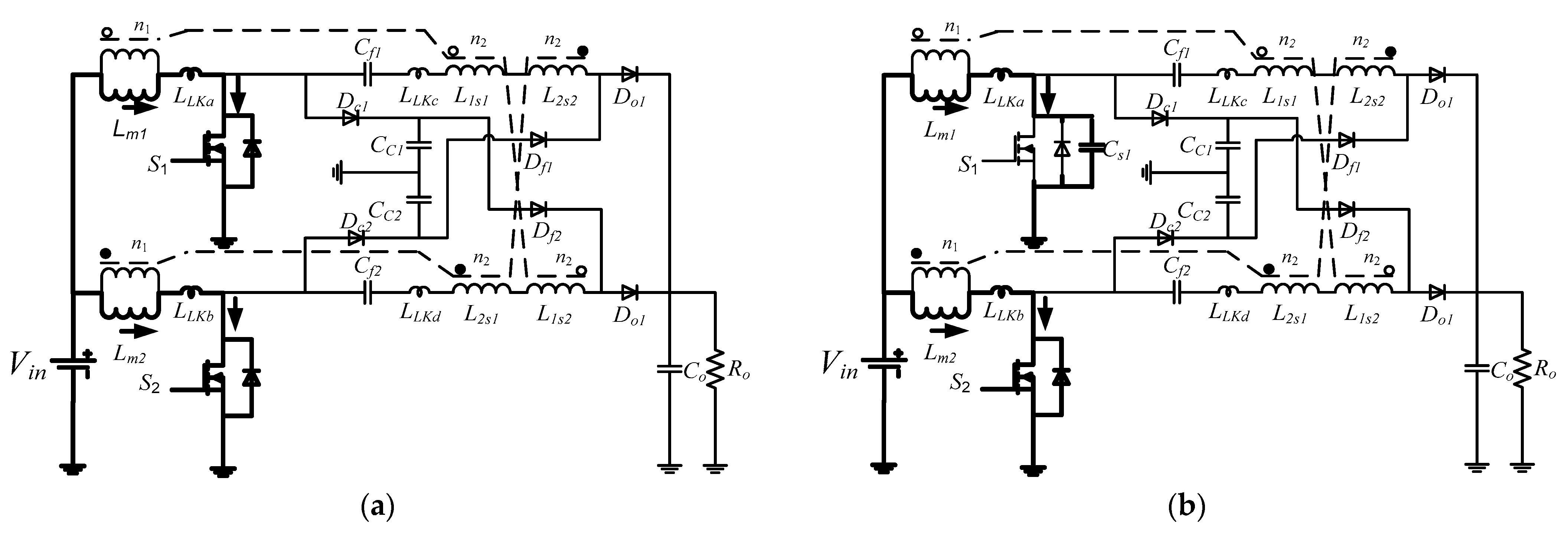
The topology of an interleaved high-step-up current sharing DC-DC converter with coupled conductors is shown in Figure 1. The traditional interleaved boost converter (low-voltage side) is shown in the left dotted framework, which uses two-phase parallel input to decrease ripples of input current and increase power level. The circuit has two coupled inductors and each one has three coils. The number of turns of the three coils in each coupled inductor are n1, n2 and n3, respectively. The dotted terminals of coupled inductors are marked by “○” and “●”. The third coil is inserted into another phase to realize current sharing performance. CC1 and CC2 are clamp capacitors which can absorb energy of leakage inductance (LLK) and reduce switch voltage stress. Cf1 and Cf2 are series capacitors. DC1 and DC2 are clamping diodes. Do1 and Do2 are output diodes, respectively.
The equivalent circuit of the interleaved high step-up current sharing converter is shown in Figure 2. Lm1 and Lm2 are excitation inductances. LLKa and LLKb are leakage inductances of primary coil of the corresponding coupled inductor. LLKc is the sum of leakage inductances in the secondary coil 2 of coupled inductor 1 and the secondary coil 3 of coupled inductor 2. LLKd is the sum of leakage inductances in the secondary coil 2 of coupled inductor 2 and the secondary coil 3 of coupled inductor 1. S1 and S2 are power switches. Vin and Vout are input voltage and output voltage. Let n2 be equal to n3 and the turns ratio (N) is determined n2/n1.
Key waveforms of the proposed converter under stable state are presented in Figure 3. There are 12 operation stages in each period. Considering the symmetrical structure of the circuit topology, only six operation stages are chosen in the following analysis.
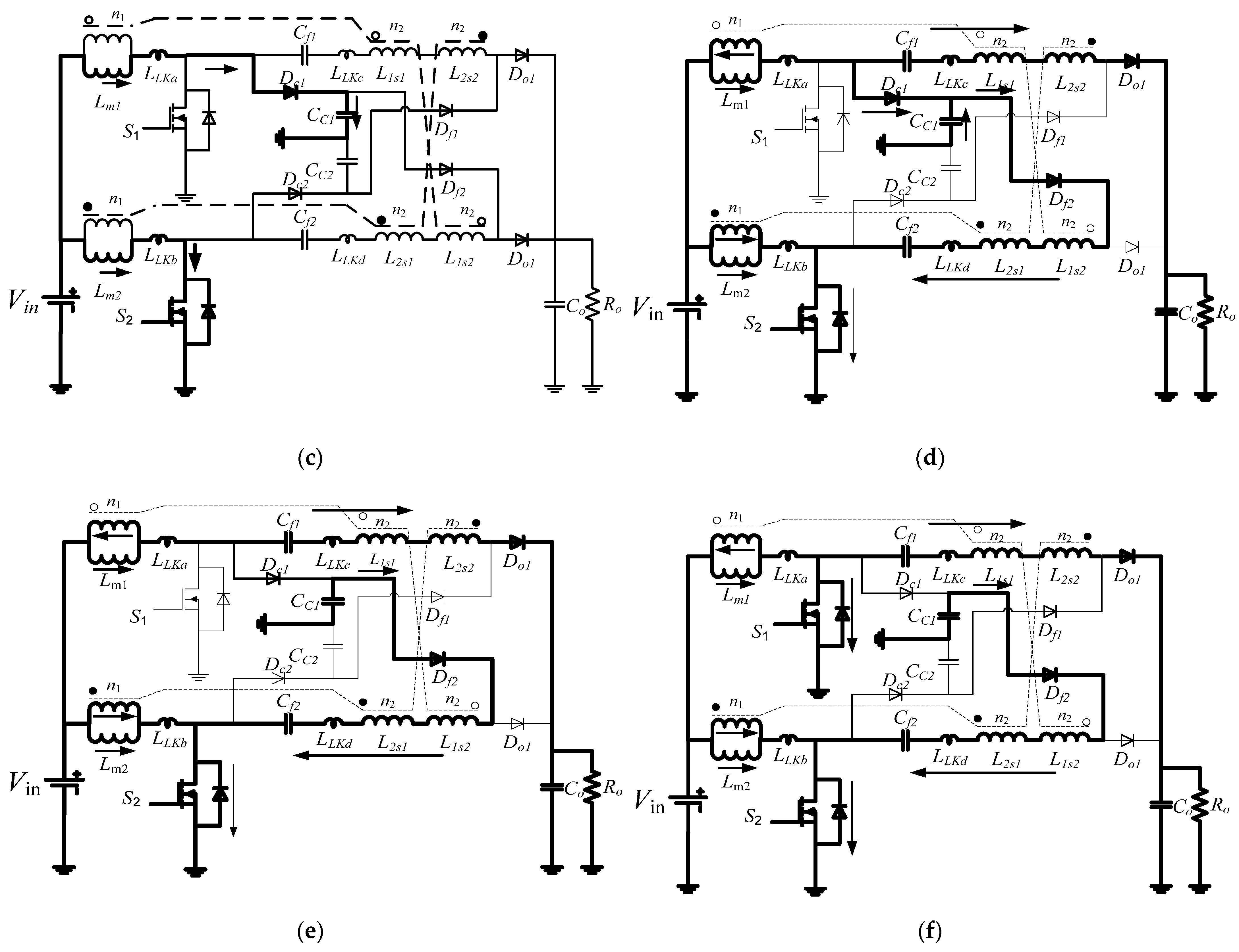
Stage 1 (t0-t1): As shown in Figure 4a, switches S1 and S2 are turned on, and diodes Do1, Do2, Dc1, Dc2, Df1 and Df2 all adopt reverse bias. The power supply is used for charging of excitation inductors (Lm1 and Lm2) and leakage inductances (Lk1 and Lk2). The rate of current rise of leakage inductance is:
d i L K a d t = V i n L L K a + L m 1
d i L K b d t = V i n L L K b + L m 2
Stage 2 (t1–t2): As shown in Figure 4b, switch s1 is turned off and the excitation inductor charges the drain-source parasitic capacitor Cs1. When the drain-source voltage is increased, the inverse voltage on diode Dc1 is decreased (Equation (3)). This operation stage is very short since the parasitic capacitance is very small.
v d s 1 ( t ) = I L m 1 ( t t 1 ) C s 1
Stage 3 (t2–t3): As shown in Figure 4c, voltage of Vds1 at t2 increased to power on the clamping diode DC1 and the excitation inductor Lm1 charges the clamp capacitor CC1. The drain-source voltage Vds1 is clamped by the clamp capacitor CC2. Energies on excitation inductor begin to be transmitted onto the clamp capacitor:
u d s 1 ( t ) = V d s 1 ( t 2 ) + I L m 1 ( t 2 ) C c 2 ( t t 2 )
Stage 4 (t3–t4): As shown in Figure 4d, since the inverse voltage of output diode Do1 at t3 decreased to zero and it is turned on, the rate of rise of the diode current is controlled by the leakage inductance LKc. The current of Dc1 declines when the current of Do1 increases. The series connection of series capacitor Cf1, the secondary coil 1 of the coupled inductor 1 and the secondary coil 2 of the coupled inductor 2 is used as the power source to get high voltage gain for the output. Meanwhile, the diode Df2 is turned on and energies which are stored on the clamping diode Cc1 are transmitted to the series capacitance Cf2 through diode Df2, secondary coil 1 of the coupled inductor 2, secondary coil 2 of the coupled inductor 1 and the switch s2. The current of diode Df2 is controlled by the leakage inductance LKd. The current relationship is as follows:
i D c 1 ( t ) = i L m 1 ( t ) ( N + 1 ) i D o 1 ( t ) N i D f 2 ( t )
Stage 5 (t4-t5): As shown in Figure 4e, current which flows through the clamping diode DC1 decreases to zero and the clamping diode DC1 is shut off. Since the rate of current reduction is controlled by leakage inductance, there is no reverse-recovery problem. Energies which are stored on the series capacitor Cf1 are transmitted onto the load. Currents which flow through Do1 are controlled by LKa and Lkc together.
Stage 6 (t5–t6): As shown in Figure 4f, the switch s1 is powered on at t5 and it realizes zero current turn-on since there’s leakage inductance (LKa). The rate of current reductions in the diode Do1 and the diode DCf2 are controlled by leakage inductances LLKc and LLKd, respectively. Therefore, there is no diode reverse-recovery problem.
i L L K a = i D c 1 + i D o 1
i S 2 = i L m 2 ( t ) + N i D o 1 ( t ) + ( N + 1 ) i i D f 2 ( t )
i D f 2 = i D f 2 ( t 5 ) V C f 2 V C C 2 L L K d ( t t 5 )
i D o 1 ( t ) = I D o 1 ( t 5 ) V o V C f 1 L L K c ( t t 5 )

3. Steady-State Working Performance Analysis

3.1. Voltage Gains

The duty cycle of signals is controlled within 0 < D < 0.5. Due to the symmetry of the circuit, there are Lm1 = Lm2, CC1 = CC2 and Cf1 = Cf2.
To simplify the analysis, voltages of the clamp capacitor (CC and series capacitor (Cf) are assumed to be stable. Hence, the voltage on the clamp capacitor is:
V c c = V i n 1 D
The voltage on Vcf can be gained from Stage 4:
V c f = 1 + N 1 D V i n
The output voltage can be gained from Stage 4:
V o = V c c 2 + V C f 1 V L 1 S 1 + V L 2 S 2
V L 1 S 1 = V i n V c c 1
V L 2 S 2 = V i n
The output voltage gain can be obtained from Equations (10)–(14):
M = 2 ( 1 + N ) 1 D
where N is the turns ratio of the coupled inductor, D is the duty cycle of switch control signals and M is the output voltage gain.
It can be seen from Equation (15) that the voltage gain of the proposed converter M is determined by duty cycle D and the turns ratio of the coupled inductor N. The relations between these two factors and voltage gain are shown in Figure 5. M is increased with the increase of D and N. In this way, it can avoid the traditional use of ultimate duty cycle in application occasions with high gains, thus decreasing the ripple of current and switching loss.

3.2. Switch Voltage Stress

Voltages on the switch S and the clamping diode DC are equal to voltage of the clamp capacitor:
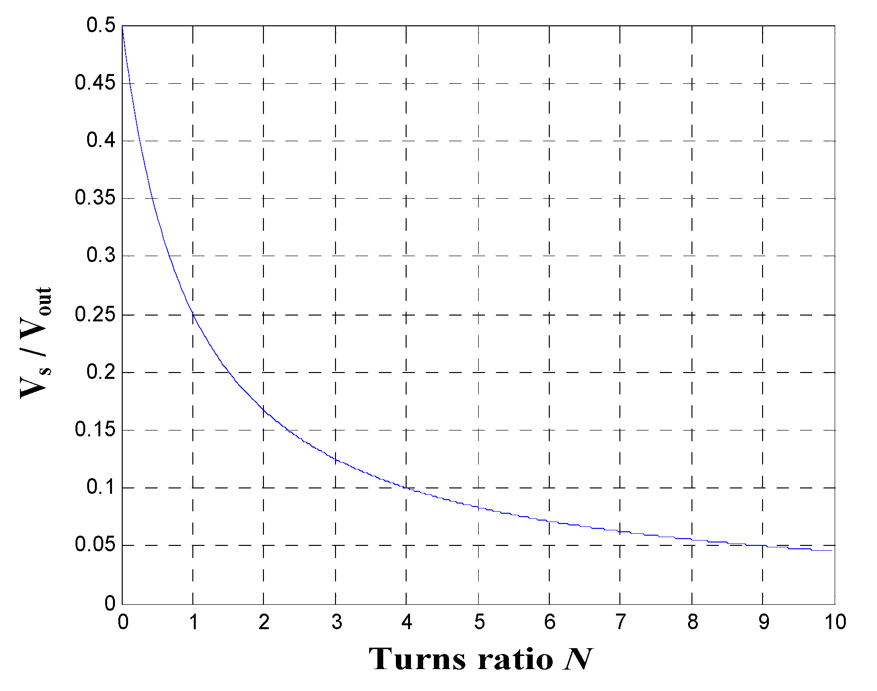
V s = V D = V i n 1 D = V o u t 2 ( 1 + N )
It can be seen from Equation (16) that when the output voltage is fixed, the voltage stress of the power switch is determined by the turns ratio of the coupled inductor. Relation curve between voltage stress and turns ratio is shown in Figure 6. The maximum voltage stress ratio is 0.5 and it declines gradually with the increase of the turns ratio. Hence, Mosfet with low rated voltage can be used in application occasions which require high gains. The lower the rated voltage is, the smaller the on-resistance is, and thus the smaller the conduction loss is.
The voltage of the series capacitor Cf is:
V c f = 1 + N 1 D V i n = V o u t 2
The voltage stress of output diode Do is:
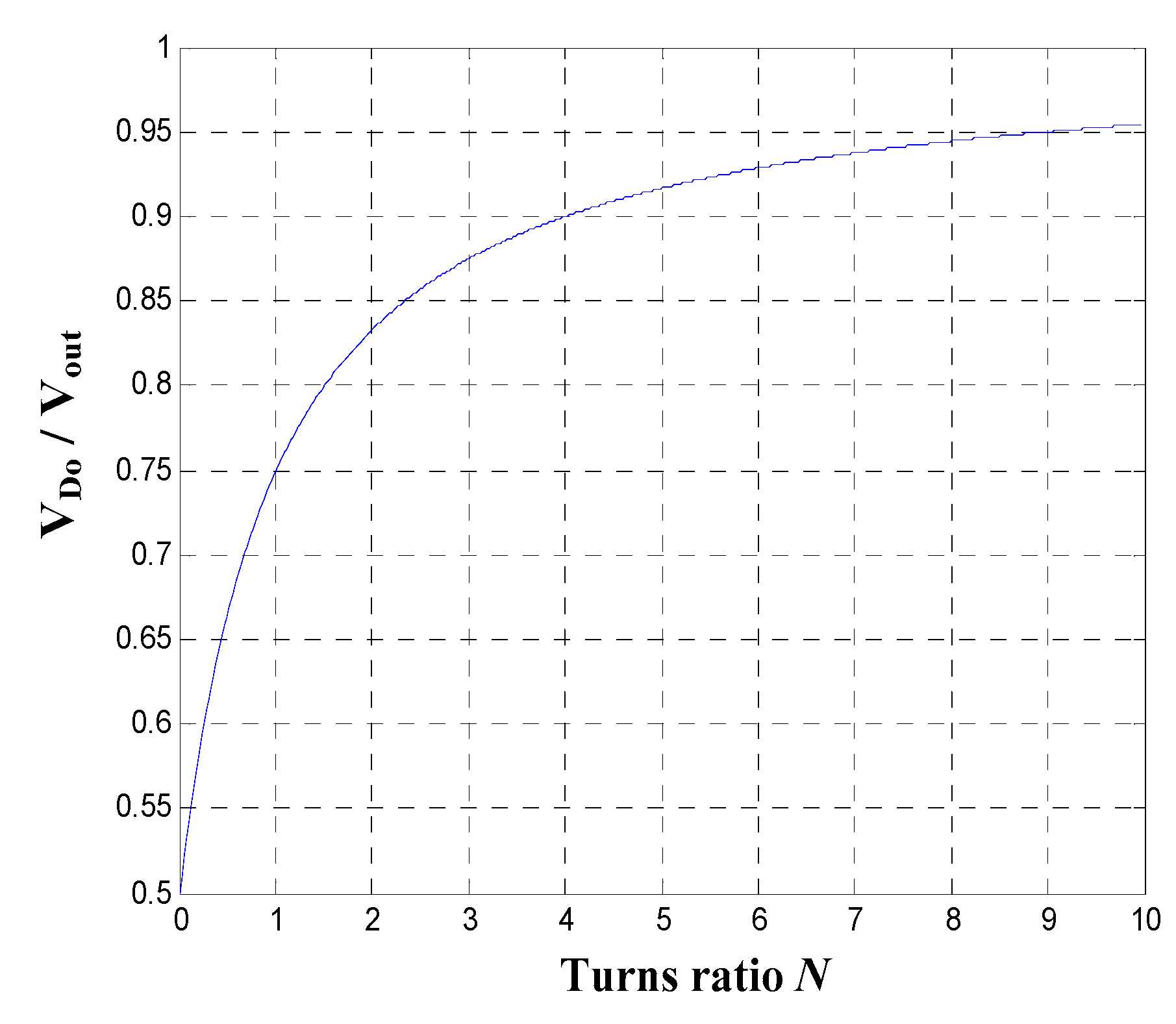
V D o = V o u t V c c = 1 + 2 N 1 D V i n = 1 + 2 N 2 ( 1 + N ) V o
The relationship between output diode voltage stress and turns ratio is shown in Figure 7. The minimum output diode voltage stress ratio is 0.5. With the increase of turns ratio, the voltage stress increases. However, it always remains lower than the output voltage.
The voltage stress of the diode Df is:
V D f = V o u t V c c = 1 + 2 N 1 D V i n = 1 + 2 N 2 ( 1 + N ) V o
This is same with the output diode voltage stress.

3.3. Realization of Soft Switching

When the switches S1 and S2 are turned on, they can realize zero-current turn on due to the effects of leakage inductances (LLKa and LLKb) of the coupled inductors. The conduction loss of switches is low. When S1 and S2 are turned off, energies which are stored in the leakage inductor are transmitted to the clamp capacitor through the clamping diode, thus significantly decreasing stress on switches and turn-off losses of the switches. Influenced by leakage inductance of the coupled inductor, the current of the clamping diode is controlled by leakage inductance and there is no reverse-recovery problem. The rate of current reduction of the output diode is controlled by LLKc and LLKd, which avoids reverse-recovery problem and decreases diode losses.

3.4. Current Sharing

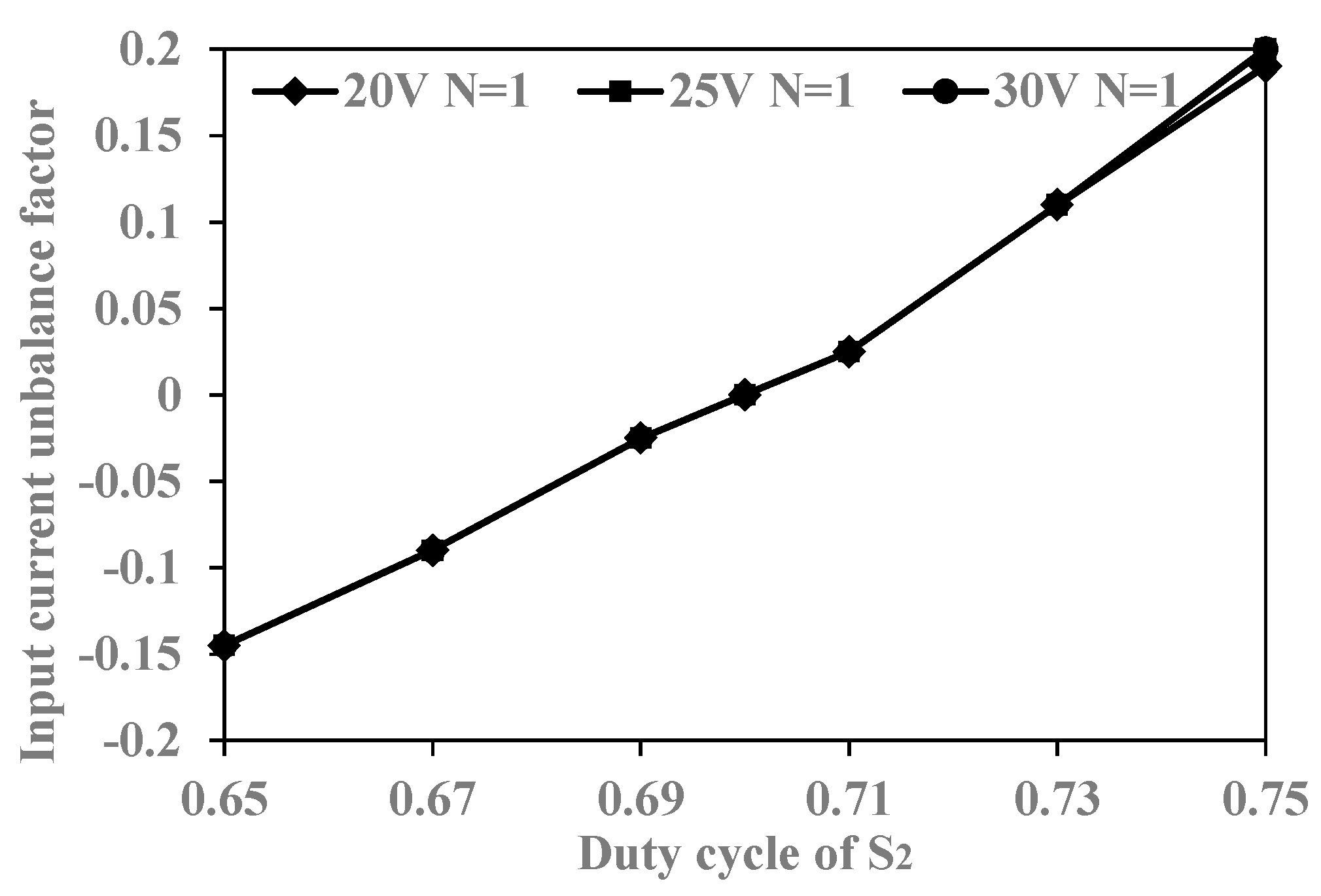
Since the third coil of the coupled inductor is inserted into another phase, two-phase current sharing can be achieved when the duty cycle is asymmetric. Simulation results of input current unbalance factor (Iin1Iin2)/Iin2 when the converter power is 1000 W, the duty ratio of S1 is 0.7 and the duty ratio of s2 increases from 0.65 to 0.75 are shown in Figure 8. Iin1 and Iin2 are primary currents of two coupled inductors. It can be seen from Figure 8 that the input current unbalance factor is very small when the duty cycle of S2 changes. When the duty cycles of S1 and S2 are 0.7 and 0.75, the input current unbalance factor is only 0.2. Simulation results of the output current unbalance factor (Io1Io2)/Io2 under the same conditions are shown in Figure 9. Io1 and Io2 are currents of two output diodes. The unbalance factor is basically zero with changes of duty ratio of S2. This circuit has very strong current sharing performances.

4. Experimental Verification

To verify the accuracy of the theoretical analysis, a 500 W prototype was used in the experimental verification. Experimental parameters of converter are introduced as follows: Vin = 20–30 V; Pout = 500 W; fs = 50 kH; n2/n1 = 16/16; Lm = 100 μH; Co = 100 μF; Cc1 and Cc2: 4.7 μF; Cf1 and Cf2: 4.7 μF; S1 and S2: IRF34158; Dc1 and Dc2: MUR1560T; Df1 and Df2: MUR1560T; Do1 and Do2: MUR1560T; duty cycle of control signals D = 0.7. Figure 10 shows the experimental setup.
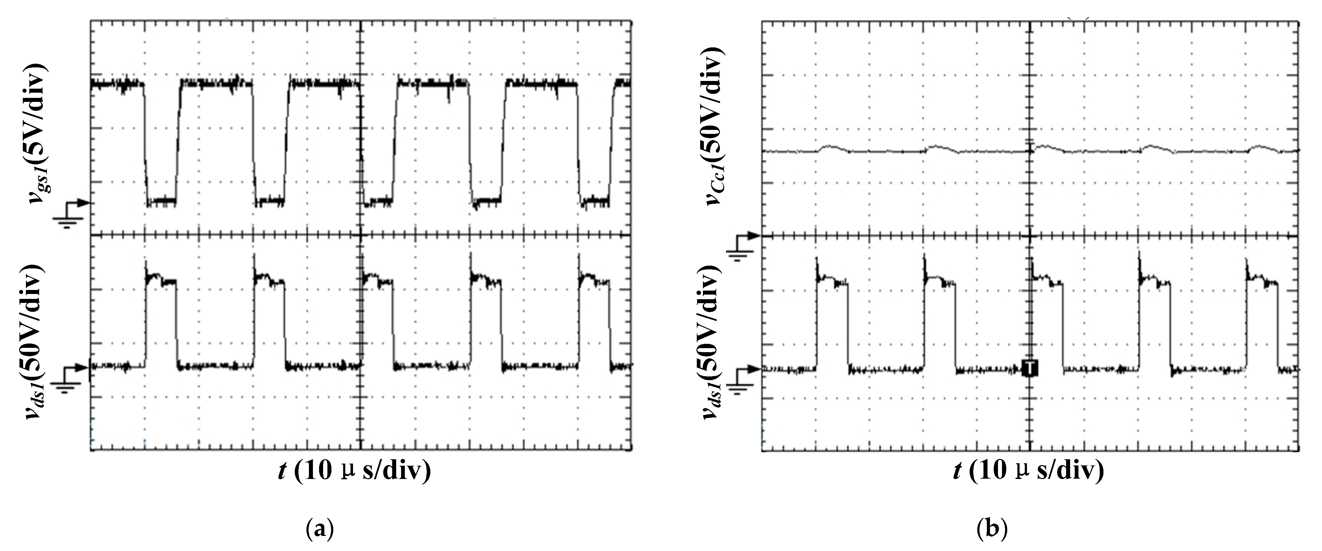
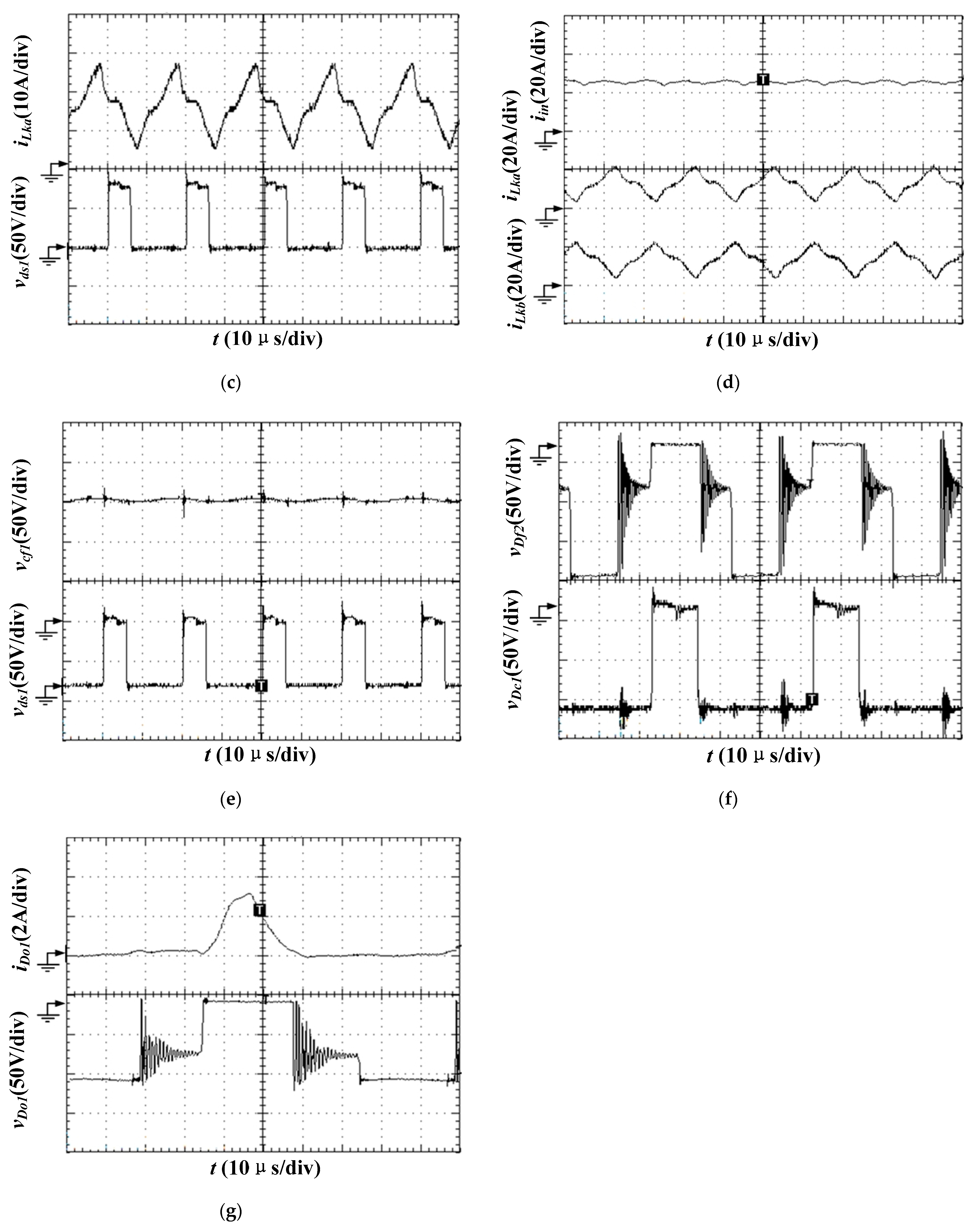
The voltage stress waveform and the driving signal waveform of S1 are shown in Figure 11a (S2 is similar to S1). Drain-source voltage of S1 is about 80 V and it is only about 1/3 of output voltage. Voltage stresses of S1 and S2 are equal. The voltage waveform of S1 and the voltage waveform of clamp capacitor C1 are shown in Figure 11b. The average voltage of C1 is about 80 V. The voltage waveform of S1 and the current waveform of leakage inductance iLKa are shown in Figure 11c. The input current waveform of the converter and current waveforms of two leakage inductances iLKa and iLkb are presented in Figure 11d. The proposed converter uses interleaved two-phase input, which decreases ripples of its input current significantly. Voltage waveform of S1 and voltage waveform of Cf1 are shown in Figure 11e. Voltage waveforms of Dc1 and Df2 are shown in Figure 11f. Voltage and current waveforms of Do1 are shown in Figure 11g, which present no reverse-recovery problem of the output diode.
The relation between the input voltage and efficiency under a closed-loop control when the output power is 500 W and the output load is constant is exhibited in Figure 12. Clearly, efficiency is positively related to the increase of input voltage. The efficiency is about 94% when the input voltage is 30 V.
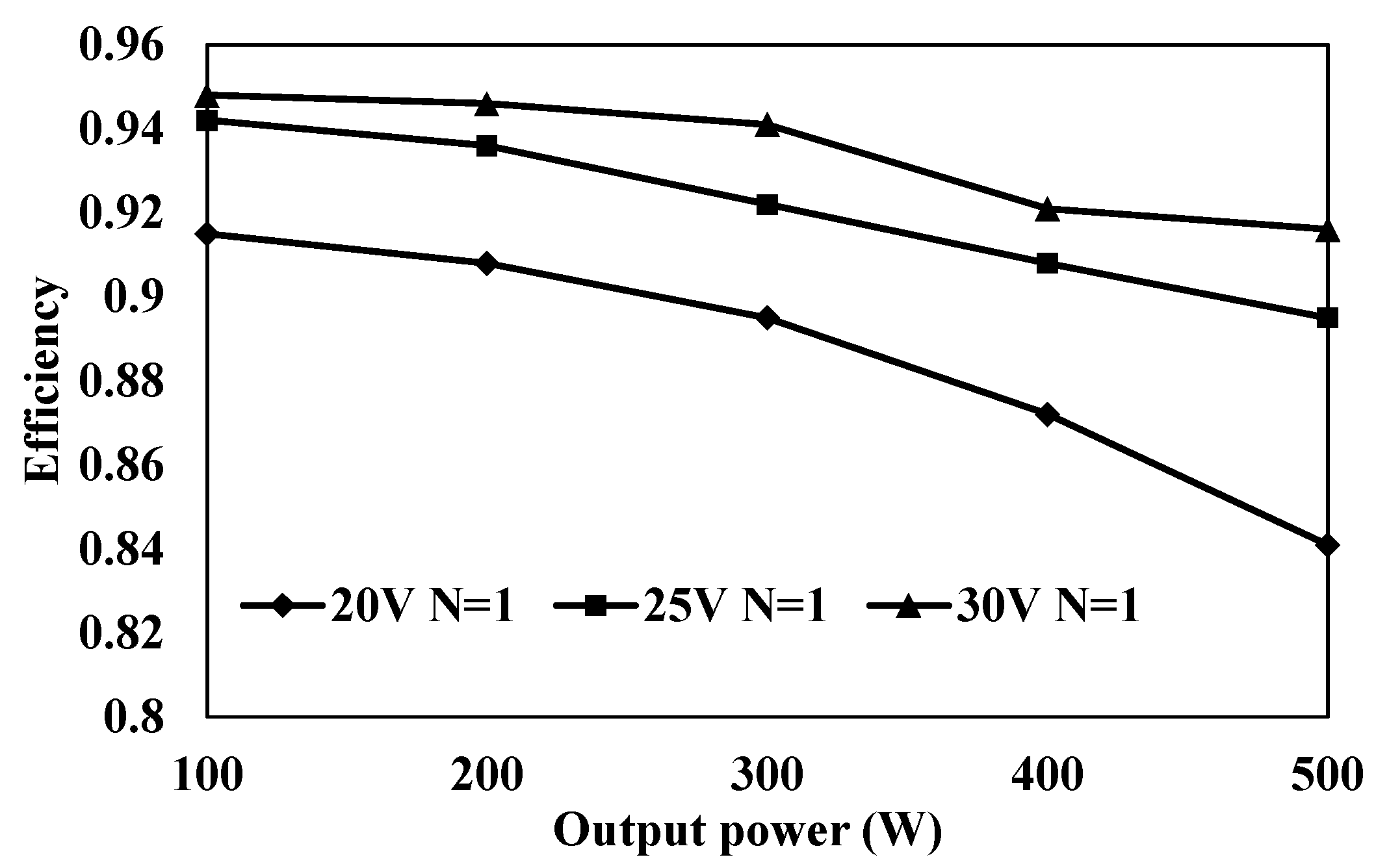
The relation between efficiency and output power when duty cycle is 0.75 and input voltages are 20 V, 25 V and 30 V is shown in Figure 13. When the output power is fixed, efficiency is positively related with input voltage. When the input voltage is fixed, efficiency is negatively correlated with output power.

5. Conclusions

An interleaved high step-up current sharing DC–DC converter with coupled conductors is proposed in this paper. Table 1 gives a performance comparison among the conventional transformer-included boost converter, the conventional interleaved boost converter, the improved interleaved boost converter described in [22] and the proposed converter. Compared to a conventional transformer-included boost converter and conventional interleaved boost converter, the proposed interleaved high step-up current sharing DC–DC converter has higher voltage gains by using the coupled inductors and voltage multiplier. Therefore, it avoids the use of ultimate duty cycle to increase voltage gain. Influenced by clamping diode and clamp capacitor, energies which are stored in leakage inductor can be recovered to the clamp capacitor, thus decreasing switch voltage stress. The proposed converter decreases ripples of input current significantly by using the parallel interleaving mode. Switches S1 and S2 realize ZCS turn on. Due to existences of leakage inductance, the reverse-recovery problem of output diode is alleviated; thus, the switching loss and electromagnetic interferences are decreased. Compared to the converter in [22], the proposed converter realized current autobalance. In addition, its clamp circuit is simpler.
There are two issues that need to be addressed in the future work. First, the switches S1 and S2 only achieve zero current turn-on. The future work is to realize zero voltage turn-off to further reduce switching loss and improve the conversion efficiency. Second, the loss of the output diode is large. The voltage stress of the output diode approaches the output voltage when the turn ratio of the coupled inductor increases. Therefore, another future work is to reduce the voltage stress of the output diode to further improve the efficiency and boost the capability of the converter.

Author Contributions

Conceptualization, L.H. and T.Z.; methodology, L.H., Z.L., Q.T., F.L. and T.Z.; software, L.H., Z.L.; validation, Q.T., F.L. and T.Z.; formal analysis, F.L.; investigation, L.H. and T.Z.; resources, L.H. and T.Z.; data curation, Q.T., F.L. and T.Z.; writing—original draft preparation, L.H. and T.Z.; writing—review and editing, L.H. and T.Z.; visualization, T.Z.; supervision, L.H. and T.Z.; project administration, L.H. and T.Z.; funding acquisition, L.H. and T.Z. All authors have read and agreed to the published version of the manuscript.

Funding

This research was funded by the Fujian Province outstanding youth fund, grant number 2018J06016, National Natural Science Foundation of China, grant number 61671400 and Guiding Project of Industrial Technology Development and Application (Fujian Science and Technology Project), grant number 2019H0004.

Conflicts of Interest

The authors declare no conflict of interest.

References

  1. D’Ovidio, G.; Masciovecchio, C.; Rotondale, A. Hydrogen fuel cell and kinetic energy recover systems technologies for powering urban bus with zero emission energy cycle. IET Intell. Transp. Syst. 2016, 10, 573–578. [Google Scholar] [CrossRef]
  2. Nemeș, R.; Ciornei, S.; Ruba, M.; Marțis, C. Real-time simulation of scaled propulsion unit for light electric vehicles. Electr. Eng. 2020, 102, 43–52. [Google Scholar] [CrossRef]
  3. Ta, L.D.; Dao, N.D.; Lee, D.C. High-efficiency hybrid LLC resonant converter for on-board chargers of plug-in electric vehicles. IEEE Trans. Power Electron. 2020, 35, 8324–8334. [Google Scholar] [CrossRef]
  4. Snoussi, J.; Elghali, S.B.; Benbouzid, M.; Mimouni, M.F. Optimal sizing of energy storage systems using frequency-separation-based energy management for fuel cell hybrid electric vehicles. IEEE Trans. Veh. Technol. 2018, 67, 9337–9346. [Google Scholar] [CrossRef]
  5. Zhang, Q.; Li, G. A predictive energy management system for hybrid energy storage systems in electric vehicles. Electr. Eng. 2019, 101, 759–770. [Google Scholar] [CrossRef]
  6. Lin, C.C.; Yang, L.S.; Wu, G. Study of a non- isolated bidirectional DC-DC converter. IET Power Electron. 2013, 6, 30–37. [Google Scholar] [CrossRef]
  7. Salvador, M.A.; Lazzarin, T.B.; Coelho, R.F. High step-up DC–DC converter with active switched- inductor and passive switched-capacitor networks. IEEE Trans. Ind. Electron. 2018, 65, 5644–5654. [Google Scholar] [CrossRef]
  8. Tseng, K.C.; Liang, T.J. Novel high-efficiency step- up converter. IEE Proc. Power Appl. 2004, 151, 182–190. [Google Scholar] [CrossRef]
  9. Narasimharaju, B.L.; Dubey, S.P.; Singh, S.P. Design and analysis of coupled inductor bidirectional DC–DC convertor for high-voltage diversity applications. IET Power Electron. 2012, 5, 998–1007. [Google Scholar] [CrossRef]
  10. Liu, H.; Wang, L.; Ji, Y.; Li, F. A novel reversal coupled inductor high-conversion-ratio bidirectional DC–DC converter. IEEE Trans. Power Electron. 2018, 33, 4968–4979. [Google Scholar] [CrossRef]
  11. Wai, R.J.; Duan, R.Y. High-efficiency power conversion for low-power fuel cell generation system. IEEE Trans. Power Electron. 2005, 20, 847–856. [Google Scholar] [CrossRef]
  12. Wai, R.J.; Duan, R.Y. High-efficiency DC/DC converter with high voltage gain. IEE Proc. Electric Power Appl. 2005, 152, 793–802. [Google Scholar] [CrossRef]
  13. Matsuda, A.; Koizumi, H.; Sato, T. Two-stage interleaved DC-DC converter with input-parallel output-series connection. In Proceedings of the IEEE International Symposium on Circuits and Systems (ISCAS), Sapporo, Japan, 26–29 May 2019; pp. 1–5. [Google Scholar]
  14. Hsieh, Y.C.; Hsueh, T.C.; Yen, H.C. An interleaved Boost converter with zero-voltage transition. IEEE Trans. Power Electron. 2009, 24, 973–978. [Google Scholar] [CrossRef]
  15. Lee, J.Y.; Kim, G.S.; Oh, K.; Baek, D. Fully integrated low-ripple switched-capacitor DC–DC converter with parallel low-dropout regulator. Electronics 2019, 8, 98. [Google Scholar] [CrossRef] [Green Version]
  16. Prabhala, V.A.K.; Fajri, P.; Gouribhatla, V.S.P.; Baddipadiga, B.P.; Ferdowsi, M. A DC–DC converter with high voltage gain and two input boost stages. IEEE Trans. Power Electron. 2016, 31, 4206–4215. [Google Scholar] [CrossRef]
  17. Frivaldsky, M.; Morgos, J.; Hanko, B.; Prazenica, M. The study of the operational characteristic of interleaved boost converter with modified coupled inductor. Electronics 2019, 8, 1049. [Google Scholar] [CrossRef] [Green Version]
  18. Alzahrani, A.; Ferdowsi, M.; Shamsi, P. A family of scalable non-isolated interleaved DC–DC boost converters with voltage multiplier cells. IEEE Access 2019, 7, 11707–11721. [Google Scholar] [CrossRef]
  19. Alzahrani, A. A hybrid DC–DC quadrupler boost converter for photovoltaic panels integration into a DC distribution system. Electronics 2020, 9, 1965. [Google Scholar] [CrossRef]
  20. Hwu, K.I.; Yau, Y.T. High step-up converter based on coupling inductor and bootstrap capacitors with active clamping. IEEE Trans. Power Electron. 2014, 29, 2655–2660. [Google Scholar] [CrossRef]
  21. Tseng, K.; Lin, J.; Huang, C. High step-up converter with three-winding coupled inductor for fuel cell energy source applications. IEEE Trans. Power Electron. 2015, 30, 574–581. [Google Scholar] [CrossRef]
  22. Li, W.; Xiang, X.; Li, C.; Li, W.; He, X. Interleaved high step-Up ZVT converter with built-in transformer voltage doubler cell for distributed PV generation system. IEEE Trans. Power Electron. 2013, 28, 300–313. [Google Scholar] [CrossRef]
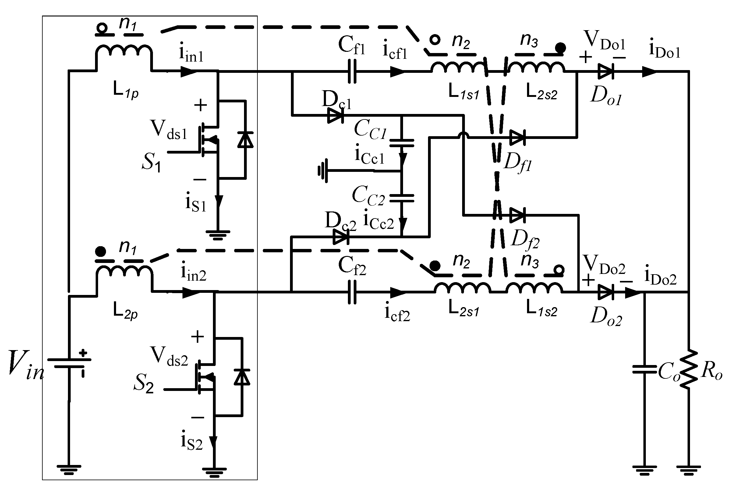
Figure 1. Interleaved high step-up current sharing converter with coupled conductors.
Electronics 10 00436 g001
Figure 2. Equivalent circuit of the interleaved high step-up current sharing converter.
Electronics 10 00436 g002
Figure 3. Key waveforms of the interleaved high step-up current sharing converter.
Electronics 10 00436 g003
Figure 4. Operation stages of the interleaved high step-up current sharing converter. (a) Stage 1. (b) Stage 2. (c) Stage 3. (d) Stage 4. (e) Stage 5. (f) Stage 6.
Electronics 10 00436 g004aElectronics 10 00436 g004b
Figure 5. Relation curves of voltage gain with turns ratio and duty cycle.
Electronics 10 00436 g005
Figure 6. Relation curve between turns ratio and normalized switch voltage stress ratio.
Electronics 10 00436 g006
Figure 7. Relation curves between turns ratio and normalized output diode voltage stress ratio.
Electronics 10 00436 g007
Figure 8. Input current auto-balance performance under asymmetrical duty cycle.
Electronics 10 00436 g008
Figure 9. Output current auto-balance performance with asymmetrical duty cycle.
Electronics 10 00436 g009
Figure 10. Experimental setup.
Electronics 10 00436 g010
Figure 11. Experimental waveforms. (a) Voltage stress waveform and the driving signal waveform of S1. (b) Voltage waveform of S1 and the voltage waveform of clamp capacitor C1. (c) Voltage waveform of S1 and the current waveform of leakage inductance. (d) Input current waveform of the converter and current waveforms of two leakage inductances. (e) Voltage waveform of S1 and voltage waveform of Cf1. (f) Voltage waveforms of Dc1 and Df2. (g) Voltage and current waveforms of Do1.
Electronics 10 00436 g011aElectronics 10 00436 g011b
Figure 12. Measured conversion efficiency under different input voltages at 500 W.
Electronics 10 00436 g012
Figure 13. Measured efficiencies at different loads.
Electronics 10 00436 g013
Table 1. Converter performance comparison.
Conventional Transformer Included Boost Converter Conventional Interleaved Boost Converter Converter in [22]Proposed Converter
Voltage gain N 2 · ( 1 D ) 1 1 D 2 + 2 N 1 D 2 + 2 N 1 D
Main switch voltage stress 2 · V o N Vo V o 2 + 2 N V o 2 + 2 N
Output diode voltage stressVoVoVoLess than 2/3 Vo
Input current rippleLargeLargeSmallsmall (in total)
Soft switchingZCS or ZVSHard switchingZVSZCS
Reverse recoveryLargeLargeSmallSmall
Output voltage rippleLargeLargeSmallSmall
Current autobalanceNoNoNoYes
Clamp circuitNatural voltage clampingAdditional circuitTwo MOSFETS
two capacitors
Two diodes
Two capacitors
Publisher’s Note: MDPI stays neutral with regard to jurisdictional claims in published maps and institutional affiliations.