Article

Prediction Model for Random Variation in FinFET Induced by Line-Edge-Roughness (LER)

1
Department of Electrical and Computer Engineering, Sungkyunkwan University, Suwon 16419, Korea
2
Department of Artificial Intelligence, Sungkyunkwan University, Suwon 16419, Korea
3
Department of Electronic and Electrical Engineering, Sungkyunkwan University, Suwon 16419, Korea
*
Authors to whom correspondence should be addressed.
Electronics 2021, 10(4), 455; https://doi.org/10.3390/electronics10040455
Submission received: 11 January 2021 / Revised: 6 February 2021 / Accepted: 9 February 2021 / Published: 12 February 2021
(This article belongs to the Section Semiconductor Devices)

Abstract

:
As the physical size of MOSFET has been aggressively scaled-down, the impact of process-induced random variation (RV) should be considered as one of the device design considerations of MOSFET. In this work, an artificial neural network (ANN) model is developed to investigate the effect of line-edge roughness (LER)-induced random variation on the input/output transfer characteristics (e.g., off-state leakage current (Ioff), subthreshold slope (SS), saturation drain current (Id,sat), linear drain current (Id,lin), saturation threshold voltage (Vth,sat), and linear threshold voltage (Vth,lin)) of 5 nm FinFET. Hence, the prediction model was divided into two phases, i.e., “Predict Vth” and “Model Vth”. In the former, LER profiles were only used as training input features, and two threshold voltages (i.e., Vth,sat and Vth,lin) were target variables. In the latter, however, LER profiles and the two threshold voltages were used as training input features. The final prediction was then made by feeding the output of the first model to the input of the second model. The developed models were quantitatively evaluated by the Earth Mover Distance (EMD) between the target variables from the TCAD simulation tool and the predicted variables of the ANN model, and we confirm both the prediction accuracy and time-efficiency of our model.

1. Introduction

In the past few decades, the physical dimension of metal oxide semiconductor field-effect transistor (MOSFET) has been dramatically decreased not only to increase the number of transistors in integrated circuits (ICs) but also to boost up the performance of transistor in ICs. As of 2020, a few billion transistors are integrated into a single piece of IC chip. However, the process-induced random variation should be considered when designing and integrating transistors in IC. It is known that the process-induced random variation is primarily occurred by three root-causes, i.e., line edge roughness (LER) [1], random dopant fluctuation (RDF) [2], and work function variation (WFV) [3].
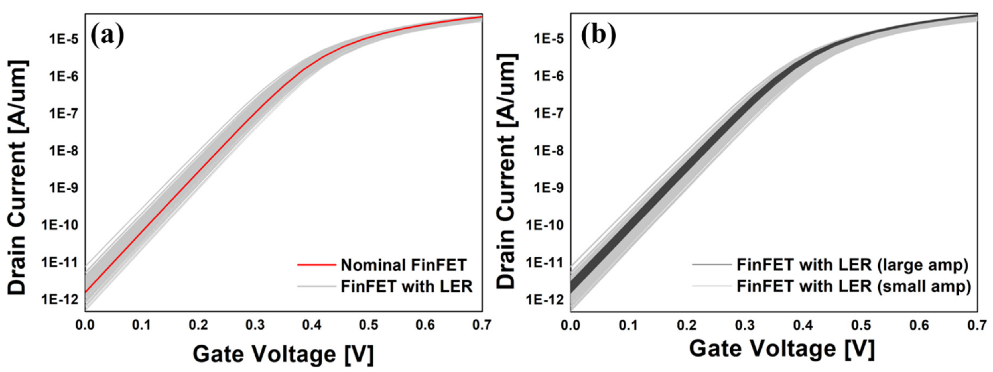
With the machine learning (ML) technique, the impact of LER-induced random variation in 5 nm FinFET is quantitatively predicted (i.e., major points in the input transfer characteristic of 5 nm FinFET (drain current-. vs.-gate voltage (Id–Vg) curve) are predicted). The major causes of LER are originated from photolithography process: (1) the line edge along the photoresist pattern is determined by the intensity of light exposure. Due to the uneven intensity, the line edge should be rough in nature. (2) Acid cations (which are generated in the deprotection process) affect the mask pattern, resulting in LER [4,5,6]. The LER profile can be characterized (and can be reconfigured) with three parameters, i.e., RMS amplitude (σ), correlation length (ξ), and roughness exponent (α) [7,8,9,10,11]. In Figure 1, an exemplary LER profile is illustrated. The RMS amplitude indicates the standard deviation of roughness along the line of the pattern. The correlation length means the “average” value of the physical distance in-between peak and valley. Note that two correlation lengths in x-/y-directions are necessary to characterize a surface roughness. In three-dimensional device structure, e.g., FinFET, two correlation lengths, i.e., x and y, are used together to reconfigure the surface roughness of sidewall in FinFET. The roughness exponent is defined as a fractal dimension. More specifically, this indicates the amount of high-frequency components left behind in LER profile [5,12,13]. Figure 2 shows the unexpected variation of FinFET’s Id–Vg curves caused by LER. In Figure 2a, the red-colored line indicates the Id–Vg curve of nominal FinFET without LER, and the gray-colored lines show Id–Vg curves of 250 FinFETs with identical LER profiles. Figure 2b shows the Id–Vg curves of FinFETs with two LER profile combinations (note that 250 cases are sampled for each case). The gray-colored lines have σ: 0.7295, ξx: 89.3916, ξy: 195.6248, and the dark gray-colored lines have σ: 0.1411, ξx: 96.7100, ξy: 186.6837. This shows that the larger the amplitude is, the larger the variation is.
In the past few years, many studies on LER-induced random variations have been done. The typical method to evaluate the effect of LER-induced random variation on FinFET device is simply to run the Technology Computer-Aided Design (TCAD) simulations with additional in-house software to implement LER [14]. However, TCAD simulations spend tens of minutes (up to hours or even days) because the total number of device-under-test should be more than a few hundred to obtain statistically significant data. In this work, to aggressively shorten the long simulation running time, an artificial neural network (ANN) is proposed and developed. We set the LER profiles as a training input feature and specify the characteristic parameters of Id–Vg curve of the device as target variables, so that perceptrons in each layer of the ANN model can learn the coefficient between them. If there is a model (which has been trained with various LER profiles), it can predict the fluctuation of Id–Vg curve within seconds.

2. Simulation

When training a machine learning (ML) model, it is necessary to prepare both training-data and test-data. In this work, those data sets were generated and obtained using TCAD (Sentaurus) and MATLAB tools. A nominal 5 nm FinFET device was designed, and it is the nominal object for the ML model. Note that the device design parameters for 5 nm FinFET device are summarized in Table 1. The quasi-atomistic model with the 2-D autocorrelation function (ACVF) method [14] (see Equation (1) below) was used to design and reconfigure the LER on the sidewall of FinFET. When creating the LER profiles, the features for the LER profiles were uniformly sampled within a limited range. Note that the range of LER profiles are as follows: σ from 0.1 nm to 0.8 nm, ξx from 10 nm to 100 nm, ξy from 20 nm to 200 nm.
A C V F x , y = σ 2 e x p x cos θ + y sin θ 2 ξ x 2 + x sin θ + y cos θ 2 ξ y 2 1 2 .
For three different LER profiles, the input transfer characteristics (i.e., Id–Vg curve) of FinFET were investigated. To investigate the impact of LER profiles on the Id–Vg characteristic of FinFET, 150 training data sets for various LER profiles were prepared (Note that a single training data set consists of 50 Id–Vg curves). We extracted 10 test data sets (consisting of 250 Id–Vg curves) out of 150 training data sets to verify the prediction model.
All data sets consist of both LER profiles (e.g., RMS amplitude (σ), x-axis correlation length (ξx), and y-axis correlation length (ξy)) and the Id–Vg curve’s characteristic parameters (e.g., off-state leakage current (Ioff), subthreshold slope (SS), the saturation drain current (Id,sat), the linear drain current (Id,lin), the saturation threshold voltage (Vth,sat), and linear threshold voltage (Vth,lin)). The scale of each data in the dataset was different from that of the other data. For example, in a test-data set, the mean of Ioff is 7.37 pA, but the mean of Vth is 299 mV. To address this issue as well as to achieve a superior learning performance, it is mandatory to have an identical scale for all the data. In the ML society, there are a few methods available for data scaling. In this work, the “Robust Scaling” method was adopted and used, because the impact of outliers on the learning performance can become minimal with the method [15].
S S = 1000 V t h V o f f log 10 I V t h / I V o f f .
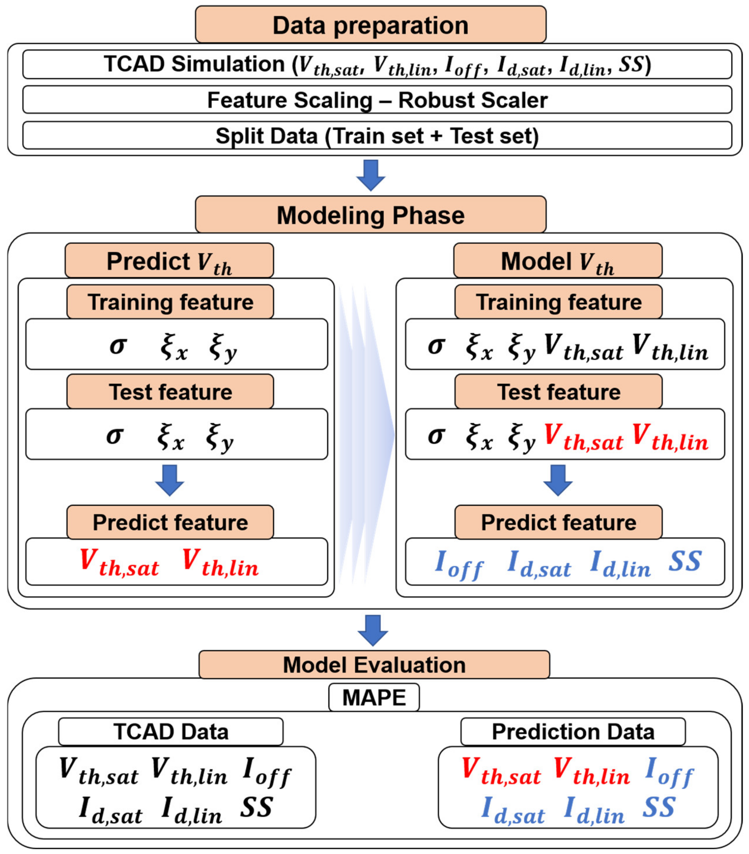
The subthreshold features (i.e., Ioff, Vth, and SS) (which are the three parameters among the six Id–Vg characteristic parameters) are physically and mathematically associated with each other (see Equation (2)). To improve the performance of the prediction model, we divided the model into two phases: (1) Predict Vth, predicting Vth using the LER profiles, and (2) Model Vth, using the LER profiles and Vth as training input features to train the coefficient of Equation (2). Figure 3 shows the overview of the prediction model.
Figure 4 shows the conceptual diagram of two artificial neural networks (ANN): (1) Predict Vth and (2) Model Vth. The input features of Model Vth are (1) 3 features for LER profiles and (2) 2 features of Vth,sat and Vth,lin (in total, 5 features). The target variables of Model Vth are the characteristic parameters of Id–Vg curve excluding Vth,sat and Vth,lin.
It is known that the LER-induced threshold voltage variation in various types of field-effect transistor follows the Gaussian distribution [1,16,17]. Based on those previous studies, the input transfer characteristics (Id–Vg curves) of FinFET should follow the multi-variate Gaussian distribution. “MultivariateNormalTril” was used to train coefficients between target variables and to improve the performance of the prediction model. It was in the last hidden layer and trained the mean vector and covariance matrix of the target variables to implement distribution. The prediction data were generated through the implemented distribution. This has been used in developing the ANN model (“Predict Vth” model).
Two ANN models consist of four hidden layers. “ReLU” was used as the active function [18]. The “batch normalization” [19] was applied to each hidden layer, and 20% of the training sets were used as the validation data sets to prevent overfitting issues. To prevent “overfitting” in the process of developing the ANN model, the “training loss” was compared against the “val loss”. Herein, the negative log-likelihood (NLL) was used as a loss function. Note that the learning process was done using “rmsprop” as an optimizer. The number of training, i.e., epoch, was set to 5000.
To validate the model, we compared the prediction results of this study and prediction results of Simple ANN using only LER profiles as training input feature.
The ANN model was designed with the built-in functions of Keras and Python using Tenserflow2.0.

3. Results and Discussion

Time spent on training is summarized in Table 2. While the running time of TCAD simulation for the FinFET used in this work was ~30 min per device, the training time for the ANN models (i.e., simple ANN and this study) was up to 35 ms per epoch. TCAD simulation needs tens of hours to make one set (250 data per set), while the ANN models need a few minutes to make 10 sets (250 data per set).
Using the developed ANN models, the LER-induced variation of threshold voltage and others (i.e., Vth,sat, Vth,lin, Id,sat, Id,lin, Ioff, and SS) of FinFET were predicted, and then compared against the test data sets. The target variables in the test set consisting of 250 data represent the form of distribution. As previous studies have shown, the LER-induced variation of threshold voltage and others of FinFET should follow the Gaussian distribution.
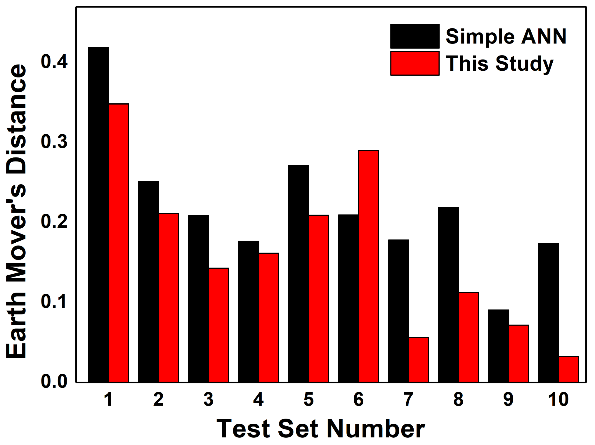
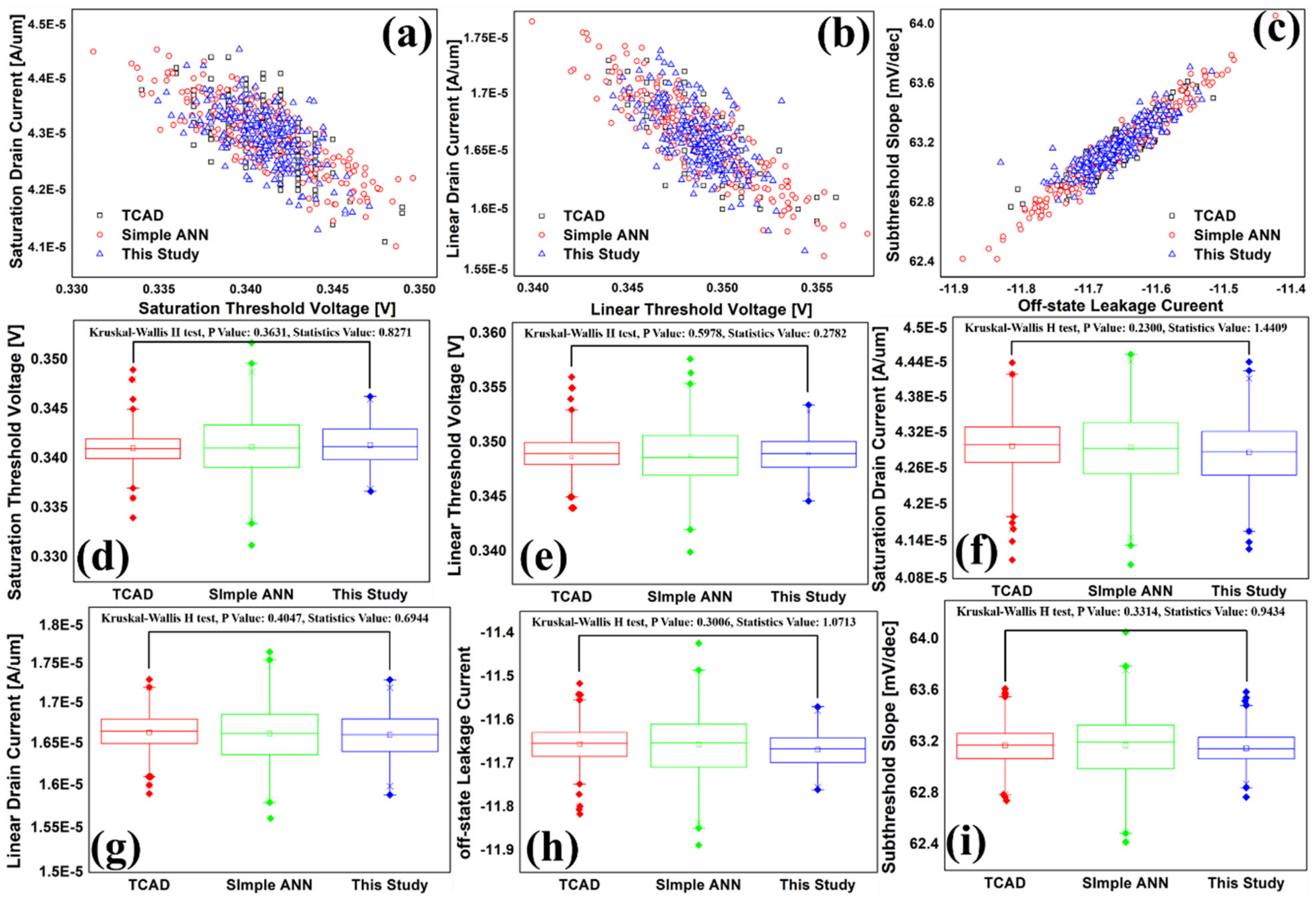
Therefore, we compared the distribution of the test set against the distribution of the prediction results of the ANN models, to evaluate the model that we developed. Using the earth mover distance (EMD) score [20], the prediction performance for each model was quantitatively evaluated. Note that EMD means “the minimum amount of work required to move from one distribution to another”. EMD can be used to compare two different distributions. The EMD scores are obtained by comparing the test data (generated by TCAD) and the prediction data (generated by the simple ANN model and the prediction model suggested in this work). The EMD score shows that the prediction model in this study has better performance than the simple ANN model. Note that the values of EMD for each model are summarized in Table 3. Figure 5 shows the bar charts of the EMD by test set number, for comparison between the simple ANN model and the proposed prediction model in this study. Except for test set 6, all EMD of the proposed model in this study is lower than the simple ANN’s. Figure 6 shows the scattering plots (a–c) and box-and-whisker plots (d–i) of the 10th test set with the largest EMD gap between the simple ANN model and the prediction model suggested in this study model. We used “the Kruskal-Wallis H test” to evaluate the statistical significance. Figure 6d–i contains the p-values obtained by the Kruskal–Wallis H test of the six characteristic parameters of Id–Vg curve. The p-value as significance level was set to 0.05 in this study.
Since the ANN prediction model in this study trained the coefficient between the subthreshold features, it would accurately predict results even with relatively few data and epoch. Considering the long running-time issue in TCAD simulation, we suggest that the ANN model can be a promising alternative to TCAD simulation, when it comes to predicting the LER-induced random variation in FinFET.

4. Conclusions

We have proposed and developed an Artificial Neural Network (ANN) model to predict the LER-induced variation of the Id–Vg curve of 5 nm FinFET. The characteristic parameters of the Id–Vg curve, which are assumed to follow the Gaussian distribution, are predicted using the suggested ANN model. The model has two phases. The first is predicting the threshold voltages of two modes using LER profiles as training input features. The second is additionally using the two threshold voltages as training input features with LER profiles to train coefficients between the subthreshold features (i.e., Ioff, Vth, and SS) and predicting the Id–Vg curve’s characteristics excluding Vth,sat and Vth,lin (e.g., Ioff, Id,sat, Id,lin, and SS).
Comparing EMD between the test data (made by TCAD simulation) and the predicted data (made by the suggested model), we demonstrate that the predicted characteristics have very similar distributions to those of TCAD data. If the distributions of the prediction model’s results are almost similar to the distribution of the TCAD data, the prediction model has much better efficiency than TCAD simulation, in terms of simulation time (i.e., the prediction model’s training time is up to 35 ms/epoch, but the TCAD simulation running time is about 30 min/device). Thus, our ML-based prediction model has accuracy and precision as the level to TCAD simulation, and are hundreds of thousands times faster than TCAD in time.
Based on the results of this study, we suggest that the ANN prediction model based on machine learning is an effective alternative to investigate the variation induced by LER of FinFET as well as to address the time-inefficiency of the TCAD simulation.

Author Contributions

Conceptualization, J.L. and C.S.; methodology, J.L.; software, J.L.; validation, J.L., T.P., H.A., J.K., T.M. and C.S.; formal analysis, J.L.; investigation, J.L., T.P, H.A., and J.K.; resources, J.L.; data curation, J.L. and C.S.; writing—original draft preparation, J.L.; writing—review and editing, T.M. and C.S.; visualization, J.L.; supervision, T.M. and C.S.; project administration, T.M. and C.S.; funding acquisition, T.M. and C.S. All authors have read and agreed to the published version of the manuscript.

Funding

This work was supported by the National Research Foundation of Korea (NRF) grant funded by the the Korean government (MSIP) (No. 2020R1A2C1009063). This work was supported by the Future Semiconductor Device Technology Development Program (20003551) funded by the Ministry of Trade, Industry and Energy (MOTIE) and the Korea Semiconductor Research Consortium (KSRC). The EDA tool was supported by the IC Design Education Center (IDEC), Korea.

Institutional Review Board Statement

Not applicable.

Informed Consent Statement

Not applicable.

Data Availability Statement

Not applicable.

Conflicts of Interest

The authors declare no conflict of interest.

References

  1. Asenov, A.; Kaya, S.; Brown, A.R. Intrinsic parameter fluctuations in decananometer MOSFETs introduced by gate line edge roughness. IEEE Trans. Electron Devices 2003, 50, 1254–1260. [Google Scholar] [CrossRef] [Green Version]
  2. Asenov, A. Random dopant induced threshold voltage lowering and fluctuations in sub-0.1/spl mu/m MOSFET’s: A 3-D “atomistic” simulation study. IEEE Trans. Electron Devices 1998, 45, 2505–2513. [Google Scholar] [CrossRef] [Green Version]
  3. Brown, A.R.; Roy, G.; Asenov, A. Poly-Si-gate-related variability in decananometer MOSFETs with conventional architecture. IEEE Trans. Electron Devices 2007, 54, 3056–3063. [Google Scholar] [CrossRef] [Green Version]
  4. Tsubaki, H.; Yamanaka, T.; Nishiyama, F.; Shitabatake, K. A study on the material design for the reduction of LWR. In Proceedings of the Advances in Resist Materials and Processing Technology XXIV, San Jose, CA, USA, 26–28 February 2007; p. 651918. [Google Scholar]
  5. Tagawa, S.; Nagahara, S.; Iwamoto, T.; Wakita, M.; Kozawa, T.; Yamamoto, Y.; Werst, D.; Trifunac, A.D. Radiation and photochemistry of onium salt acid generators in chemically amplified resists. In Proceedings of the Advances in Resist Technology and Processing XVII, Santa Clara, CA, USA, 28 February–1 March 2000; pp. 204–213. [Google Scholar]
  6. Prabhu, V.M.; Vogt, B.D.; Kang, S.; Rao, A.; Lin, E.K.; Satija, S.K.; Turnquest, K. Direct measurement of the in-situ developed latent image: The residual swelling fraction. In Proceedings of the Advances in Resist Materials and Processing Technology XXIV, San Jose, CA, USA, 26–28 February 2007; p. 651910. [Google Scholar]
  7. Constantoudis, V.; Patsis, G.; Tserepi, A.; Gogolides, E. Quantification of line-edge roughness of photoresists. II. Scaling and fractal analysis and the best roughness descriptors. J. Vac. Sci. Technol. B Microelectron. Nanometer Struct. Process. Meas. Phenom. 2003, 21, 1019–1026. [Google Scholar] [CrossRef]
  8. Patsis, G.P.; Constantoudis, V.; Tserepi, A.; Gogolides, E.; Grozev, G.; Hoffmann, T. Roughness analysis of lithographically produced nanostructures: Off-line measurement and scaling analysis. Microelectron. Eng. 2003, 67, 319–325. [Google Scholar] [CrossRef]
  9. Constantoudis, V.; Patsis, G.P.; Gogolides, E. Photoresist line-edge roughness analysis using scaling concepts. J. Micro/Nanolithogr. MEMS MOEMS 2004, 3, 429–436. [Google Scholar] [CrossRef]
  10. Yamaguchi, A.; Tsuchiya, R.; Fukuda, H.; Komuro, O.; Kawada, H.; Iizumi, T. Characterization of line-edge roughness in resist patterns and estimations of its effect on device performance. In Proceedings of the Metrology, Inspection, and Process Control for Microlithography XVII, Santa Clara, CA, USA, 24–27 February 2003; pp. 689–698. [Google Scholar]
  11. Bunday, B.D.; Bishop, M.; Villarrubia, J.S.; Vladar, A.E. CD-SEM measurement line-edge roughness test patterns for 193-nm lithography. In Proceedings of the Metrology, Inspection, and Process Control for Microlithography XVII, Santa Clara, CA, USA, 24–27 February 2003; pp. 674–688. [Google Scholar]
  12. Wang, X.-B.; Ferris, K.; Wang, L.-S. Photodetachment of gaseous multiply charged anions, copper phthalocyanine tetrasulfonate tetraanion: Tuning molecular electronic energy levels by charging and negative electron binding. J. Phys. Chem. A 2000, 104, 25–33. [Google Scholar] [CrossRef]
  13. Stewart, M.D.; Tran, H.V.; Schmid, G.M.; Stachowiak, T.B.; Becker, D.J.; Willson, C.G. Acid catalyst mobility in resist resins. J. Vac. Sci. Technol. B Microelectron. Nanometer Struct. Process. Meas. Phenom. 2002, 20, 2946–2952. [Google Scholar] [CrossRef] [Green Version]
  14. Oh, S.; Shin, C. 3-D quasi-atomistic model for line edge roughness in nonplanar MOSFETs. IEEE Trans. Electron Devices 2016, 63, 4617–4623. [Google Scholar] [CrossRef]
  15. Burke, S. Missing values, outliers, robust statistics & non-parametric methods. Sci. Data Manag. 1998, 1, 32–38. [Google Scholar]
  16. Baravelli, E.; Dixit, A.; Rooyackers, R.; Jurczak, M.; Speciale, N.; De Meyer, K. Impact of line-edge roughness on FinFET matching performance. IEEE Trans. Electron Devices 2007, 54, 2466–2474. [Google Scholar] [CrossRef]
  17. Chen, Y.-N.; Chen, C.-J.; Fan, M.-L.; Hu, V.P.-H.; Su, P.; Chuang, C.-T. Impacts of work function variation and line-edge roughness on TFET and FinFET devices and 32-bit CLA circuits. J. Low Power Electron. Appl. 2015, 5, 101–115. [Google Scholar] [CrossRef] [Green Version]
  18. Bircanoğlu, C.; Arıca, N. A comparison of activation functions in artificial neural networks. In Proceedings of the 2018 26th Signal Processing and Communications Applications Conference (SIU), Izmir, Turkey, 2–5 May 2018; pp. 1–4. [Google Scholar]
  19. Ioffe, S.; Szegedy, C. Batch normalization: Accelerating deep network training by reducing internal covariate shift. arXiv 2015, arXiv:1502.03167. [Google Scholar]
  20. Rubner, Y.; Tomasi, C.; Guibas, L.J. A metric for distributions with applications to image databases. In Proceedings of the Sixth International Conference on Computer Vision (IEEE Cat. No. 98CH36271), Bombay, India, 7 January 1998; 56, pp. 59–66. [Google Scholar]
Figure 1. A line-edge roughness (LER) profile can be characterized with three key features such as rms amplitude (σ), correlation length (ξ), and roughness exponent (α).
Electronics 10 00455 g001
Figure 2. (a) Drain current-. vs.-gate voltage (Id–Vg) curves of FinFET with LER vs. nominal FinFET. (b) Id–Vg curves of FinFET with LER but with different amplitudes.
Electronics 10 00455 g002
Figure 3. Overview of the prediction model.
Electronics 10 00455 g003
Figure 4. Conceptual diagram of two artificial neural networks (ANN): (1) Predict Vth (see top left-side one) and (2) Model Vth (see top right-side one). Note that two threshold voltages (Vth,sat and Vth,lin) and LER profiles (σ, ξx, and ξy) as training features are used as input for the Model Vth.
Electronics 10 00455 g004
Figure 5. The earth mover distance (EMD) scores between the test sets (made by Technology Computer-Aided Design (TCAD)) and the prediction data sets (made by the simple artificial neural network (ANN) model and the prediction model suggested in this study).
Electronics 10 00455 g005
Figure 6. Scattering plots (ac) of test data (made by TCAD) and prediction results (made by simple ANN and the ANN model proposed in this study). (di) Box-and-whisker plots (di) of electrical characteristics in Id–Vg for test data (made by TCAD) as well as for the prediction results (made by simple ANN and the ANN model proposed in this study). Note that the Kruskal–Wallis H test’s values (i.e., p-value and statistics value) are included.
Electronics 10 00455 g006
Table 1. Device design parameters of the FinFET used in this work.
Device Parameters
SymbolDescriptionUnitValue
LgGate lengthnm20
ToxEquivalent oxide thickness (HfO2)nm0.3
WfinFin widthnm7
HfinFin heightnm50
VDDPower supply voltageV0.7
IVtiConstant currentA/um5.35 × 10−7
σRMS amplitudenm0.1~0.8
ξxx-axis correlation lengthnm10~100
ξyy-axis correlation lengthnm20~200
Table 2. Time spent on training.
ModelTime
Simple ANN 450 s (15,000 epoch)
This studyPredict Vth100 s (5000 epoch)
Model Vth175 s (5000 epoch)
Table 3. The EMD of each model.
TEST SETAmp.Corr. xCorr. yEMD
Simple ANN10.624817.0074173.85720.419317
20.556580.919180.56990.251837
30.504748.624067.99380.208757
40.560525.428769.39740.176496
50.637369.148665.33040.271804
60.729589.3916195.62480.209605
70.152723.326451.25330.178308
80.689985.088680.98370.219300
90.259378.126528.08680.090672
100.141196.7100186.68370.174057
Average EMD0.220015
This Study10.624817.0074173.85720.348625
20.556580.919180.56990.211269
30.504748.624067.99380.143110
40.560525.428769.39740.161759
50.637369.148665.33040.209351
60.729589.3916195.62480.290165
70.152723.326451.25330.056710
80.689985.088680.98370.112868
90.259378.126528.08680.071807
100.141196.7100186.68370.032418
Average EMD0.163808
Publisher’s Note: MDPI stays neutral with regard to jurisdictional claims in published maps and institutional affiliations.