Abstract
A transformer-based voltage-controlled oscillator for a W-band frequency-modulated continuous-wave (FMCW) automotive radar application is presented. The design challenges imposed by the millimeter-wave frequency operation were faced through a circuit and layout co-design approach, supported by extensive electromagnetic simulations and accurate analysis of both the start-up condition and the tank quality factor. The oscillator was implemented in a 28-nm fully depleted silicon-on-insulator (SOI) complementary metal–oxide–semiconductor (CMOS) technology. It provided a 37 GHz oscillation frequency with a variation of around 4 GHz, thus achieving a tuning range of 11%. Moreover, a 77 GHz output signal was also delivered, which was extracted as a second harmonic from the input-pair common-mode node. The circuit exhibited low phase noises, whose average performances were −97 dBc/Hz and −121 dBc/Hz at 1 MHz and 10 MHz offset frequencies, respectively. It delivered a 77-GHz output power of −10.5 dBm and dissipated 26 mW with a 1 V power supply. The silicon area occupation was 300 × 135 µm.
1. Introduction
Long- and short-range sensing techniques have experienced strong development in recent years thanks to the growing interest expressed for them by the automotive industry. Presently, the implementation of the most common functions of an advanced driver assistance system (ADAS) for safety and security involves several kinds of sensors, such as light detection and ranging (LIDAR), camera, ultrasound, and millimeter-wave (mm−wave) radar. Among them, mm-wave radar sensors, which are mostly based on the frequency−modulated continuous−wave (FMCW) technique, have gained high interest due to their low size and robustness against environmental influences. Nowadays, complementary metal–oxide–semiconductor (CMOS) technologies with a low power supply and a high integration level that enables system-on-chip (SoC) solutions are the most promising candidates for low-cost mm-wave radar integrated circuits.
A common ADAS implementation involves radar sensors with different resolutions and operating distance requirements. To meet them while constraining the whole system cost, multimode radar solutions are preferred. They can support both long-range radar (LRR; from 76 to 77 GHz) and short-range radar (SRR; from 77 to 81 GHz) operation modes, thus avoiding the need for different radar devices. A multimode radar needs a frequency synthesizer with a wide frequency tuning range and high spectral purity to enable high-resolution sensing for short-range operation and accurate detection of low-level reflected signals for long-range operation, respectively. Specifically, modern radar sensors must be able to guarantee an operating distance ranging from a few meters to about 250 m with a resolution better than 5 cm during short-range operation. This calls for a frequency synthesizer with a tuning range wider than 3 GHz and a phase noise better than −90 dBc/Hz with a 1 MHz offset frequency [1,2].
In a voltage-controlled oscillator (VCO)-based frequency synthesizer, these requirements are largely determined by the VCO itself, which is one of the most critical building blocks in an integrated mm-wave radar transceiver. In truth, when designing a VCO, stringent tradeoffs between various performance parameters must be considered, such as the phase noise (PN), frequency tuning range (TR), start-up robustness, power consumption, and area. The design of VCOs that are capable of simultaneously achieving a low PN and a wide TR is a very challenging task, especially at mm-wave frequencies. Indeed, as the VCO oscillation frequency increases, the quality factor of passive components (capacitors, inductors, and varactors) decreases, with a negative impact on both the PN and power consumption. In addition, the need for larger transistors to support the oscillation and the consequent larger interconnection area give rise to heavy parasitic capacitance contributions, which greatly impact the TR, especially when a low supply voltage is used. Therefore, W-band CMOS VCOs exhibit a poor trade-off between PN and TR performance [1,3].
To partially overcome these limitations, a VCO followed by a frequency multiplier is used to produce the operating frequency [2,4]. By setting the VCO oscillation frequency to be much lower than the required operating frequency, it allows for passive components with a higher quality factor, thus guaranteeing a better PN/TR trade-off. Moreover, a VCO with a lower oscillation frequency simplifies the phase-locked loop (PLL) implementation since it relaxes the pre-scaler design and prevents the system from being affected by power amplifier (PA) pulling effects. For this purpose, a commonly adopted solution is to set the oscillation frequency at half the operating frequency (i.e., at around 38 GHz) and extract the second harmonic component from a common-mode node of the oscillator [5,6]. Moreover, transformer-based topologies can be profitably exploited at mm-wave frequencies since they show the advantage of a better PN, thanks to an enhanced resonator Q-factor, as is shown below. To increase the VCO tuning range, switched resonators (i.e., switched-capacitor or switched-inductor resonators) are used [7]. However, special care must be spent on the switch losses and parasitic capacitances, which could impact the resonator Q-factor and the tuning range, respectively. Moreover, most of these approaches introduce a delay in the frequency tuning, which is not compatible with an FMCW radar application.
Several performance-enhancing techniques have been proposed in the literature in the last decade to improve the PN in the transformer-based VCO topology. Among them, waveform shaping using the second [8,9] and third [10,11] harmonic resonances in a harmonically tuned tank is the most interesting. Although these techniques can effectively improve the oscillator PN, their use at mm-wave frequencies is not so straightforward and does not always lead to reliable solutions.
In this paper, the design of a transformer-based VCO is presented, which was implemented in a 28-nm fully depleted silicon-on-insulator (FD–SOI) CMOS technology for W-band automotive radar applications. The paper is structured as follows. In Section 2, both the VCO start-up condition and the resonator Q-factor are analyzed with the aim of minimizing the PN while simultaneously guaranteeing a robust start-up. A design procedure for a mm-wave VCO and the details of the circuit implementation are discussed in Section 3. The measurements are presented in Section 4 and the conclusion follows in Section 5.
2. VCO Analysis
Figure 1a shows the schematic of the proposed VCO. It consists of a transformer-based topology with an oscillating core at 38 GHz. The resonator is built around the integrated transformer, T1, which enhances the Q-factor and provides a positive feedback path from the drains to the gates of the cross-coupled differential pair, M1,2. To compensate for the process, voltage and temperature (PVT) tuning reduction, the VCO was designed to cover about 4 GHz of frequency tuning range (37–41 GHz), which is higher than the nominal tuning range of 2.5 GHz required by the radar application. Accumulation-MOS (A-MOS) varactors, CV, and single-ended control voltage, VC, were adopted.
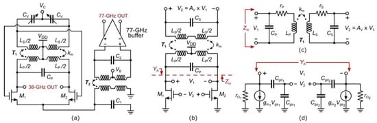
Figure 1.
(a) Simplified schematic of the proposed voltage-controlled oscillator (VCO). (b) Transformer-based VCO equivalent circuit. (c) Transformer-based tank. (d) Small-signal active core equivalent circuit.
As shown in Figure 1a, the 77-GHz signal is picked up at the common source node of M1,2 using transformer T2, whose primary and secondary winding resonances are tuned at the second harmonic of the VCO oscillation frequency. This signal is applied to a buffer that delivers it to the output with the desired power level. Note that the resonance at the first coil of T2 provides a high-impedance path between the differential pair and ground at the second harmonic of the oscillation signal. This resonance prevents the differential pair from loading the tank when M1 or M2 are pushed into the triode region, thus avoiding PN degradation.
Finally, the 38-GHz VCO output that drives the PLL prescaler is drawn from the primary winding of transformer T1.
2.1. Start-Up Condition
To analyze the start-up condition, the proposed VCO in Figure 1a can be replaced with the equivalent circuit in Figure 1b. Here, voltage V2 at the secondary side of T1 is equal to voltage V1 at the primary side multiplied by the voltage gain, , provided by the transformer. Voltage V2 is also the voltage across the gates of transistors M1,2. Therefore, the equivalent circuit in Figure 1b can be divided into the transformer-based tank and the active core, as shown in Figure 1c,d, respectively. The resistances and in Figure 1c account for the losses in the primary and secondary windings of T1, whereas capacitors CP and CS include a resonant capacitor and the varactor at the primary and secondary winding, respectively, besides parasitic capacitance contributions at the gate and drain of the input pair. The MOS parameters in Figure 1d have the usual meaning.
The input impedance, , the transimpedance, , and the voltage gain, , of this network are calculated in (1)–(3), respectively, for . They are fourth-order transfer functions with two pairs of complex conjugate poles, which account for the resonances at the primary and secondary windings. Assuming that the coupled inductors LP and LS have a sufficiently high quality factor at the operating frequency, i.e., and , the two resonant frequencies can be written as in (4).
where:
and is the magnetic coupling coefficient.
The transconductance that satisfies the start-up condition can be found by evaluating the small-signal admittance, , across the drain nodes of transistors M1,2, as shown in Figure 1d. Considering the feedback provided by T1 that is expressed by gain , is given by:
Equation (6) reveals that the equivalent transconductance of the differential pair is boosted by the transformer voltage gain. By evaluating (1) and (3) for and combining them with (6), the constraint on the couple pair transconductance, , imposed by the start-up condition can be given as follows:
where is the transformer turn ratio. As expected, the primary coil inductance and quality factor play a key role in the start-up condition.
It is interesting to note that the transconductance in (7) is negative only for . Therefore, the oscillation never occurs at the higher frequency .
2.2. Tank Quality Factor
It is well-known that the tank Q-factor plays a key role in the start-up condition, as well as in the oscillator PN performance. PN at the oscillation frequency, , as a function of the offset frequency, , is well described in the region by the Leeson’s formula [12]:
where F is the oscillator excess noise factor, V0 is the oscillation amplitude, RT is the tank equivalent parallel resistance, and QT is the overall tank quality factor. As is apparent from (8), a tank with a high Q is mandatory for a low PN, and hence, it is very important to understand how the design parameters should be set to optimize the tank Q-factor.
Considering that for , the imaginary part of the frequency response in (2) is negligible and assuming , QT can be written as:
Equation (10) gives the resonator Q-factor as a function of the primary and secondary coil quality factors, QP and QS, coupling coefficient , and parameter . Figure 2 shows QT, evaluated at , as a function of and for different values of and /.
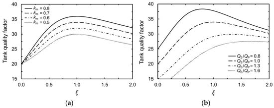
Figure 2.
Tank Q-factor evaluated at as a function of for different values of (a) and (b) the ratio .
As is apparent in Figure 2a, the resonator Q-factor increases with . In a typical design, the transformer coils are assumed to have the same Q (i.e.,) [14], hence the maximum tank Q-factor, , is achieved for and is given by:
According to (11), the tank Q-factor is increased by a factor with respect to the single-inductor Q-factor. Moreover, is equal to when . Although is a usual design condition, the value of that maximizes QT depends in general on the ratio , as is apparent in Figure 2b. Indeed, by keeping constant and increasing , increases and reaches the maximum value for according to (10). Considering the optimal value of , a useful design strategy for tank optimization can be drawn from (5). For a given transformer T1, the maximum is achieved by properly setting the primary and secondary coil capacitances CP and CS. Specifically, rewriting (4) as a function of , CP, and CS can be expressed as:
Finally, the minimum transconductance value, , is given by:
Equation (14) is obtained by substituting (10) into (7). As expected, it shows the relationship of the inverse proportionality that binds to .
3. VCO Design
As mentioned before, the VCO was designed as a 28-nm FD-SOI CMOS technology, which uses a general-purpose low-cost back-end-of-line (BEOL) consisting of eight copper metal layers, whose thicker ones are the last two (referred to as IB and IA) and an aluminum metal layer (LB) at the top of the stack. The previous analysis was adopted, which is summarized in the design flow in Figure 3.
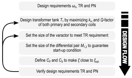
Figure 3.
Proposed design flow.
Maximization of the resonator Q-factor is a key design point for low PN and a robust start-up condition, as highlighted in Section 2. For a given operating frequency, depends on the parameters and , as shown in (10), and achieves its maximum, , if the condition is satisfied.
increases with and the Q-factor of both the primary and secondary windings of T1. Moreover, a higher also reduces the minimum transconductance for the start-up condition, as is apparent in (14). This, in turn, leads to a smaller size of the input pair and hence to smaller parasitic capacitances. To achieve a high , the stacked configuration for the tank transformer was adopted.
As is well known, low inductance and large capacitance should be used in the tank to minimize PN [1,4]. However, this approach leads to a low equivalent parallel loss resistance in the tank, which reduces the oscillator loop gain and hence entails the use of larger transistors to guarantee the start-up. This results in an increase in the parasitic capacitances, which limit the oscillator tuning range. Therefore, the sizes of the primary and secondary coil inductances of the transformer tank must be considered as part of a trade-off between PN performance, tuning range, and power consumption.
Figure 4 shows a 3-D view of the VCO tank transformer, along with the adopted metal stack and its main parameters. The transformer was implemented by adopting a single turn octagonal winding with a stacked configuration, whose inner diameter and metal width were 65 µm and 25 µm, respectively.
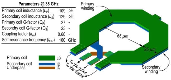
Figure 4.
3-D view of transformer T1 with the adopted metal stack.
To minimize both the resistive losses and parasitic capacitances from the substrate, an aluminum layer LB and an upper copper metal layer IB were used for the primary and secondary windings, respectively, while a metal layer IA was used for the underpass. Moreover, neither polysilicon nor a metal patterned ground shield (PGS) was used in the transformer design since it has a negligible impact on substrate losses at mm-wave frequencies [15] but significantly reduces the self-resonant frequency. The whole transformer structure was designed using the 2.5-D electromagnetic (EM) simulator “Momentum,” by including interconnections and supply/ground paths, with the aim of maximizing the Q-factor of both primary and secondary coils.
A-MOS varactors were profitably used to meet the TR requirement. Unfortunately, varactors exhibit a poor Q-factor at mm-wave frequencies, which is the main hindrance regarding the resonator quality factor. Therefore, varactors must be designed to be as small as possible, even though this is in contrast with the TR performance. Thanks to the transformer tank implementation that was adopted, the transformer turn ratio, n, was slightly higher than 1, and hence the varactors could be advantageously placed between the transistor gates. Indeed, the capacitance variation at the secondary winding was equivalently increased by a factor n. This allowed for a smaller varactor to be used to cover the tuning range, with the benefit of a reduced amplitude-to-phase noise conversion due to the varactor nonlinearity [6]. According to the previous consideration, a small A-MOS varactor connected to the secondary winding of transformer T1 was used, which provided a capacitance ranging from 40 fF to 80 fF and a Q-factor around 14 at 38 GHz. Due to the underpass that performed the cross-connection of the transformer with the gates, the secondary winding of T1 exhibited higher losses, although the overall tank Q-factor was dominated by the varactors. Using (10) and assuming that was close to its optimal value, an equivalent tank Q-factor around 33 was achieved, which was higher than that of the transformer inductors.
As far as the differential pair is concerned, the size was set by considering that a larger transistor width provides a robust start-up condition but increases the thermal noise and parasitic capacitances, which affect PN and TR, respectively.
The layout at mm-wave frequencies greatly impacts the performance of a VCO in terms of PN and TR. Therefore, accurate layout design becomes mandatory to minimize parasitic effects, especially gate resistance and gate-to-drain capacitances [16]. For this purpose, extensive EM and post-layout simulations were carried out to select the size of the transistor pair, whose aspect ratio was set to 28 µm/100 nm. Moreover, a multifinger transistor with double gate contacts was used in this design. Indeed, each transistor finger is a distributed RC network and a double contact reduces the resistance of each finger by a factor of four, thus reducing the equivalent thermal noise.
To set close to its optimal value, CP and CS must be set according to (12) and (13), respectively. For this design, CP and CS had overall values of 102 fF and 64 fF, respectively, which accounted for the parasitic, additional, and varactor capacitances, as mentioned before.
Transformer T2 at the source node of the differential pair was designed using similar layout considerations to those of T1 but with the aim of minimizing the insertion loss (IL) at 77 GHz. For this purpose, an interstacked configuration was preferred [15,17], whose 3-D view is shown in Figure 5, along with the transformer’s main parameters. Both the primary and secondary windings were implemented with upper metal layers IA, IB, and LB by adopting a spiral width of 5.5 µm, which allowed for a good trade-off between the winding parasitic capacitances and series resistance to be achieved. The winding metal spacing was set to the minimum value (i.e., 2 µm) to improve the magnetic coupling coefficient that was involved in the signal transfer and the inner diameter was set to 30 µm.
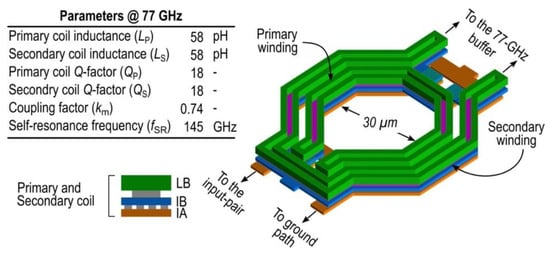
Figure 5.
3-D view of transformer T2 with the adopted metal stack.
4. Experimental Results
The 38 GHz VCO was implemented in the 28-nm FD-SOI CMOS technology by STMicroelectronics, which provided a fast active device with and up to 300 GHz [18] and a general-purpose BEOL.
The chip was assembled with the chip-on-board approach in an FR4 printed circuit board (PCB). The measurement setup is shown in Figure 6. Frequency dividers and a buffer were also included in the test chip (see the dashed area in Figure 6), which was mounted in the PCB, together with a commercial phase-frequency detector and charge pump (PFD/CP) and a discrete loop filter (LF) to enable closed-loop measurements at 4.8 GHz.
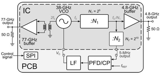
Figure 6.
Simplified block diagram of the measurement setup.
Figure 7 shows the die microphotograph. The total die area was 1660 × 1280 µm, including the electrostatic discharge (ESD) protection ring and the radio frequency (RF) ground–signal–ground (GSG) pads, whereas the VCO core area was only 300 × 135 µm.
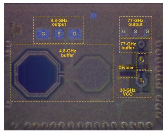
Figure 7.
Die microphotograph.
The current consumptions of the VCO, divider, and testing buffer were 26, 30, and 4.5 mA, respectively, from a 1 V power supply. The measured tuning range was 4 GHz (i.e., from 35 to 39 GHz) when the varactor control voltage VC swept from 0 to 1 V, as shown in Figure 8a. The comparison with the simulated curve highlighted a frequency shift of around 2 GHz, which could mainly be ascribed to the first tentative varactor model available at the time of the VCO design.
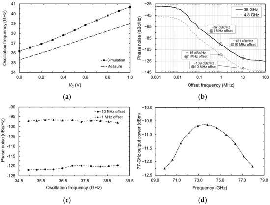
Figure 8.
Measured (a) frequency tuning range, (b) phase noise, (c) phase noises at the 1 MHz and 10 MHz offset frequencies versus the VCO oscillation frequency, and (d) 77-GHz output power.
The measured VCO phase noise is illustrated in Figure 8b. The PNs at 4.8 GHz were −115 dBc/Hz and −139 dBc/Hz at the 1 MHz and 10 MHz offset frequencies, respectively. The extrapolated curve at 38 GHz is also shown in Figure 8b, which was calculated from the assumption of a PN degradation factor of using a frequency division ratio of . At a 38 GHz oscillation frequency, the equivalent PNs were about −97 dBc/Hz and −121 dBc/Hz at the 1 MHz and 10 MHz offset frequencies, respectively. The measured VCO phase noise at 1 MHz and 10 MHz over the whole frequency tuning range is shown in Figure 8c. In these curves, the best, average, and worst PNs at a 1 MHz offset frequency were −96.6 dBc/Hz, −97 dBc/Hz, and −98 dBc/Hz, respectively, whereas the best, average, and worst PNs at a 10 MHz offset frequency were −122 dBc/Hz, −121 dBc/Hz, and −120 dBc/Hz, respectively.
Figure 8d shows the measured second harmonic output power as a function of the tuning voltage. The output power at 77 GHz varied between −12.2 dBm and −10.6 dBm in the entire frequency range.
Table 1 provides a summary of the measured results and a comparison with state-of-the-art mm-wave CMOS VCOs. To consider the oscillator’s main performance parameters, a comparison was also carried out by considering the well-known figure of merits, FoM and FoMT.

Table 1.
Performance summary and comparisons with the state of the art.
By normalizing the PN according to its typical dependence on the oscillation frequency expressed in (8), the proposed VCO exhibited the best performance regarding the PN, with the exception of [20], whose output frequency was achieved by exploiting the third harmonic of a 10 GHz oscillator. Specifically, the PN performance at a 10 MHz offset frequency, which is the most critical PN requirement for an automotive radar sensor, achieved an excellent value of −121 dBc/Hz. Regarding the FoMs, the proposed VCO showed similar values to the state-of-the-art oscillators.
5. Conclusions
A transformer-based VCO topology for FMCW automotive radar applications was discussed. Thanks to an accurate design strategy for the Q-factor maximation of the transformer-based tank, a low phase noise was achieved while preserving the oscillation tuning range, despite an oscillation frequency as high as 38 GHz. Indeed, the phase noise performance at a 10 MHz offset frequency achieved an excellent performance of −121 dBc/Hz, where this is the most important requirement for the radar maximum operating distance.
The VCO was implemented in a 28-nm FD-SOI CMOS technology, along with a prescaler and a frequency divider for test purposes. Although the technology adopted a standard BEOL to achieve low fabrication costs and a 38 GHz oscillation frequency was performed, the measured phase noise was better than that of most state-of-the-art mm-wave CMOS oscillators. The VCO was able to directly drive a PA stage since it provided a 77-GHz buffered signal with an output power higher than −12 dBm in the whole tuning range.
Author Contributions
Conceptualization, A.C. and G.P. (Giuseppe Papotto); methodology, A.C. and G.P. (Giuseppe Papotto); validation, A.P., C.N., and A.F.; formal analysis, A.C. and G.P. (Giuseppe Papotto); investigation, A.C.; writing—original draft preparation, A.C.; writing—review and editing, A.C. and G.P. (Giuseppe Palmisano); supervision, G.P. (Giuseppe Palmisano); project administration, G.P. (Giuseppe Palmisano). All authors have read and agreed to the published version of the manuscript.
Funding
This work was supported by the University of Catania as part of the project “Ricerca di Ateneo UNICT 2020-22” and by STMicroelectronics.
Acknowledgments
A special thank is given to A. Castorina, STMicroelectronics, Catania, for the measurement assistance.
Conflicts of Interest
The authors declare no conflict of interest.
References
- Sapone, G.; Ragonese, E.; Italia, A.; Palmisano, G. A 0.13-µm SiGe BiCMOS Colpitts-Based VCO for W-Band Radar Transmitters. IEEE Trans. Microw. Theory Techn. 2013, 61, 185–194. [Google Scholar] [CrossRef]
- Ma, T.; Deng, W.; Chen, Z.; Wu, J.; Zheng, W.; Wang, S.; Qi, N.; Liu, Y.; Chi, B. A CMOS 76–81-GHz 2-TX 3-RX FMCW Radar Transceiver Based on Mixed-Mode PLL Chirp Generator. IEEE J. Solid-State Circuits 2020, 55, 233–248. [Google Scholar] [CrossRef]
- Xu, J.; He, K.; Wang, Y.; Zhang, R.; Zhang, H. A 79.1–87.2 GHz 5.7-mW VCO With Complementary Distributed Resonant Tank in 45-nm SOI CMOS. IEEE Microw. Wireless Comp. Lett. 2019, 29, 477–479. [Google Scholar] [CrossRef]
- Padovan, F.; Tiebout, M.; Mertens, K.L.R.; Bevilacqua, A.; Neviani, A. Design of Low-Noise K-Band SiGe Bipolar VCOs: Theory and Implementation. IEEE Trans. Circuits Syst. I Reg. Pap. 2015, 62, 607–615. [Google Scholar] [CrossRef]
- Chao, Y.; Luong, H.C.; Hong, Z. Analysis and Design of a 14.1-mW 50/100-GHz Transformer-Based PLL With Embedded Phase Shifter in 65-nm CMOS. IEEE Trans. Microw. Theory Techn. 2015, 63, 1193–1201. [Google Scholar] [CrossRef]
- Koo, H.; Kim, C.; Hong, S. Design and Analysis of 239 GHz CMOS Push-Push Transformer-Based VCO With High Efficiency and Wide Tuning Range. IEEE Trans. Circuits Syst. I Reg. Papers 2015, 62, 1883–1893. [Google Scholar] [CrossRef]
- Basaligheh, A.; Saffari, P.; Filanovsky, I.M.; Moez, K. A 65–81 GHz CMOS Dual-Mode VCO Using High Quality Factor Transformer-Based Inductors. IEEE Trans. Circuits Syst. I Reg. Pap. 2020, 67, 4533–4543. [Google Scholar] [CrossRef]
- Shahmohammadi, M.; Babaie, M.; Staszewski, R.B. A 1/f Noise Upconversion Reduction Technique for Voltage-Biased RF CMOS Oscillators. IEEE J. Solid-State Circuits 2016, 51, 2610–2624. [Google Scholar] [CrossRef]
- Murphy, D.; Darabi, H.; Wu, H. Implicit Common-Mode Resonance in LC Oscillators. IEEE J. Solid-State Circuits 2017, 52, 812–821. [Google Scholar] [CrossRef]
- Pepe, F.; Andreani, P. A General Theory of Phase Noise in Transconductor-Based Harmonic Oscillators. IEEE Trans. Circuits Syst. I Reg. Pap. 2017, 64, 432–445. [Google Scholar] [CrossRef]
- Zong, Z.; Babaie, M.; Staszewski, R.B. A 60 GHz Frequency Generator Based on a 20 GHz Oscillator and an Implicit Multiplier. IEEE J. Solid-State Circuits 2016, 51, 1261–1273. [Google Scholar] [CrossRef]
- Leeson, D.B. A simple model of feedback oscillator noise spectrum. Proc. IEEE 1966, 54, 329–330. [Google Scholar] [CrossRef]
- Razavi, B. A study of phase noise in CMOS oscillators. IEEE J. Solid-State Circuits 1996, 31, 331–343. [Google Scholar] [CrossRef]
- Mazzanti, A.; Bevilacqua, A. On the Phase Noise Performance of Transformer-Based CMOS Differential-Pair Harmonic Oscillators. IEEE Trans. Circuits Syst. I Reg. Pap. 2015, 62, 2334–2341. [Google Scholar] [CrossRef]
- Cavarra, A.; Nocera, C.; Papotto, G.; Ragonese, E.; Palmisano, G. Transformer design for 77-GHz down-converter in 28-nm FD-SOI CMOS Technology. Lect. Notes Electr. Eng. (ApplePies 2018) 2019, 550, 195–201. [Google Scholar]
- Zhao, D.; Reynaert, P. A 60-GHz Dual-Mode Class AB Power Amplifier in 40-nm CMOS. IEEE J. Solid-State Circuits 2013, 48, 2323–2337. [Google Scholar] [CrossRef]
- Nocera, C.; Cavarra, A.; Ragonese, E.; Palmisano, G.; Papotto, G. Down-converter solutions for 77-GHz automotive radar sensors in 28-nm FD-SOI CMOS technology. In Proceedings of the 14th Conf. on Ph.D. Research in Microelectronics and Electronics (PRIME), Prague, Czech Republic, 2–5 July 2018; pp. 153–156. [Google Scholar]
- Cathelin, A. Fully depleted silicon on insulator devices CMOS: The 28-nm node is the perfect technology for analog, RF, mmW, and mixed-signal system-on-chip integration. IEEE Solid-State Circuits Mag. 2017, 9, 18–26. [Google Scholar] [CrossRef]
- Haghi Kashani, M.; Tarkeshdouz, A.; Molavi, R.; Sheikholeslami, A.; Afshari, E.; Mirabbasi, S. On the Design of a High-Performance mm-Wave VCO With Switchable Triple-Coupled Transformer. IEEE Trans. Microw. Theory Techn. 2019, 67, 4450–4464. [Google Scholar] [CrossRef]
- Hu, Y.; Siriburanon, T.; Staszewski, R.B. A Low-Flicker-Noise 30-GHz Class-F23 Oscillator in 28-nm CMOS Using Implicit Resonance and Explicit Common-Mode Return Path. IEEE J. Solid-State Circuits 2018, 53, 1977–1987. [Google Scholar] [CrossRef]
- Chen, Z.; Wang, M.; Chen, J.X.; Liang, W.F.; Yan, P.P.; Zhai, J.F.; Hong, W. Linear CMOS LC -VCO Based on Triple-Coupled Inductors and Its Application to 40-GHz Phase-Locked Loop. IEEE Trans. Microw. Theory Techn. 2017, 65, 2977–2989. [Google Scholar] [CrossRef]
- Mammei, E.; Monaco, E.; Mazzanti, A.; Svelto, F. A 33.6-to-46.2 GHz 32 nm CMOS VCO with −177.5 dBc/Hz minimum noise FOM using inductor splitting for tuning extension. In Proceedings of the 2013 IEEE International Solid-State Circuits Conference Digest of Technical Papers, San Francisco, CA, USA, 17–21 February 2013; pp. 350–351. [Google Scholar]


Publisher’s Note: MDPI stays neutral with regard to jurisdictional claims in published maps and institutional affiliations. |
© 2021 by the authors. Licensee MDPI, Basel, Switzerland. This article is an open access article distributed under the terms and conditions of the Creative Commons Attribution (CC BY) license (http://creativecommons.org/licenses/by/4.0/).