Article

System Level Simulation of Microgrid Power Electronic Systems

Department of Mechatronics and Electronics, Faculty of Electrical Engineering and Information Technologies, University of Zilina, Univerzitna 1, 010 26 Zilina, Slovakia
*
Author to whom correspondence should be addressed.
Electronics 2021, 10(6), 644; https://doi.org/10.3390/electronics10060644
Submission received: 28 January 2021 / Revised: 17 February 2021 / Accepted: 5 March 2021 / Published: 10 March 2021

Abstract

:
In this paper, we describe a procedure for designing an accurate simulation model using a price-wised linear approach referred to as the power semiconductor converters of a DC microgrid concept. Initially, the selection of topologies of individual power stage blocs are identified. Due to the requirements for verifying the accuracy of the simulation model, physical samples of power converters are realized with a power ratio of 1:10. The focus was on optimization of operational parameters such as real-time behavior (variable waveforms within a time domain), efficiency, and the voltage/current ripples. The approach was compared to real-time operation and efficiency performance was evaluated showing the accuracy and suitability of the presented approach. The results show the potential for developing complex smart grid simulation models, with a high level of accuracy, and thus the possibility to investigate various operational scenarios and the impact of power converter characteristics on the performance of a smart gird. Two possible operational scenarios of the proposed smart grid concept are evaluated and demonstrate that an accurate hardware-in-the-loop (HIL) system can be designed.

1. Introduction

Global electricity consumption has been rising from year to year, and the current distribution system is no longer adequately covering the consumption and other requirements of energy consumers, mainly in densely populated agglomerations, or in built-up industrial zones, where many large energy consumers are concentrated. If the network limits are exceeded, in extreme cases, the power supply is interrupted a so-called distribution system “blackout”. The solution to this problem could be a new generation network, i.e., a “smart grid” [1,2,3,4].
Nowadays, more and more governments, environmental activists, and other environmental organizations are pushing for the use of green renewable energy sources (RES). The primary approach is very simple, stop using fossil fuels and redirect the industry and households to use RES. The strong development of the green and alternative or renewable energy systems has been intensively investigated for almost a decade. In most of the European countries, it has occurred since 2008, when the European Union’s effort to introduce mandatory RES shares in the energy sector for all EU member states culminated. The last European Union strategy “Energy 2020” directive stipulated a 20% decrease in CO2 emissions, a 20% increase in the use of renewable sources, and a 20% increase in energy efficiency by 2020 [5,6,7,8,9]. Currently, the member states are already on track to meet the greenhouse emissions reduction target for 2020, while the forward plan is to cut emissions by at least 55% by 2030 [10].
The increasing penetration of renewable energy resources and new sizeable loads, such as electric vehicle (EV) charging stations, has posed many technical and operational challenges in the distribution grids [11,12]. Encouraged by attractive tariffs and promotional policies, the end-consumers in the local grids are not only consumers of electricity but in many cases also producers. The actual electric distribution system limits the penetration of renewable energy resources and is based on a unidirectional information flow from sources to control centers. With a gradual deployment and a combination of various energy sources with the possibility of cooperation with the public grid, the development of so-called intelligent or smart grids has been started. Power electronics solutions in the latest technologies can control the electric power flow in a wide range of conditions, and therefore have made the implementation of the widely discussed concept of smart grids possible [13,14,15].
Therefore, smart grid (SG) networks are suitable in cases where many generators (traditional power plants), storage tanks (supercapacitors and EVs), or domestic microgrids are connected to the network, as well as where a two-way flow of energy is required and where the management of energy flows is necessary in order to achieve a goal (for example, economic profit). With the help of SG networks, we can also ensure a significant reduction in transmission losses by moving energy over short distances, which leads to a reduction in conductivity losses. Figure 1 shows an example of a home SG network model with its own DC microgrid (unidirectional intermediate circuit) and an intelligent electronic transformer. The domestic microgrid also contains energy accumulators in the form of lead-acid accumulators and a domestic hot water (DHW) tank. Some devices can also be connected directly to a DC microgrid if they are adapted to do so. The sources of renewable energy in the network are amorphous photovoltaic panels and, in the future, we can also consider electric car batteries as a source/storage of energy [16].
From the abovementioned description, it is evident that smart grids and their future concepts represent complex systems composed of many power semiconductor systems. In addition, it should be noted that a major challenge in the proper operation of such systems is the optimal management and mutual communication within the smart grid subsystem if various energy flow control plans are considered [17]. A common way to investigate and research different operational schemes of SG is to utilize a hardware-in-the-loop simulation approach. It allows us to use the advantages of rapid prototyping, flexibility, and versatility with no potential risk of harming the hardware, because the entire power stage (power semiconductor converters, energy storage systems, etc.) of a smart grid is substituted using equivalent computer models. In this way, it is possible to eliminate time-consuming reconfigurations during testing, or increased costs during system developments [18]. However, the limitation of HIL modeling is the lack of real behavior and impact of equipment that is usually hard to fully capture in a simulation environment [19]. Therefore, the potential for studying HIL modeling of smart grids is using a combination of advanced validation techniques interfacing the real and virtual environments, i.e., real-time simulation, hardware-in-the-loop control, and power stage representation reaching real physical behavior of modeled systems [20,21,22].
In this paper, we describe a proposed design for an HIL model of a smart grid, mainly aimed at developing highly accurate simulation models of individual smart grid system components, with the requirement that the calculation speed must be as low as possible. Such an approach should enable researchers to investigate various concepts of operational scenarios of SG even if standard PC technology is used. Therefore, we have designed a simulation of the power stages of a SG, and we validated the modeling approach using experimental measurements. The proposed model is evaluated by comparing it with real-time behavior (time waveforms of circuit variables) together with an evaluation of the accuracy of qualitative system indicators such as efficiency. Initially, a circuit description of individual power converters for DC microgrid subsystems (i.e., photovoltaic maximum power point tracking (MPPT) converter, bidirectional DC-DC converter, and grid inverter) is modeled using a piecewise linear electric circuit simulator (PLECS) simulator. The results of time-waveform operations are compared to experimental samples of converters, while to verify the accuracy of the HIL models, the efficiency of simulation models and experimental samples are compared for a wide operational range. At the end of the paper, the HIL simulation model of the proposed SG is given. Two operational scenarios regarding SG power flow are initially tested as an example of the potential use and possible analyzes of the proposed modeling approach. The main contribution of the presented research is also represented by the methodology of the modeling, which utilizes simplified piecewise linear electrical circuit models of the power stages, which is beneficial if the computation speeds of SG complex simulation analyses are provided (i.e., various operational scenarios of power flow).

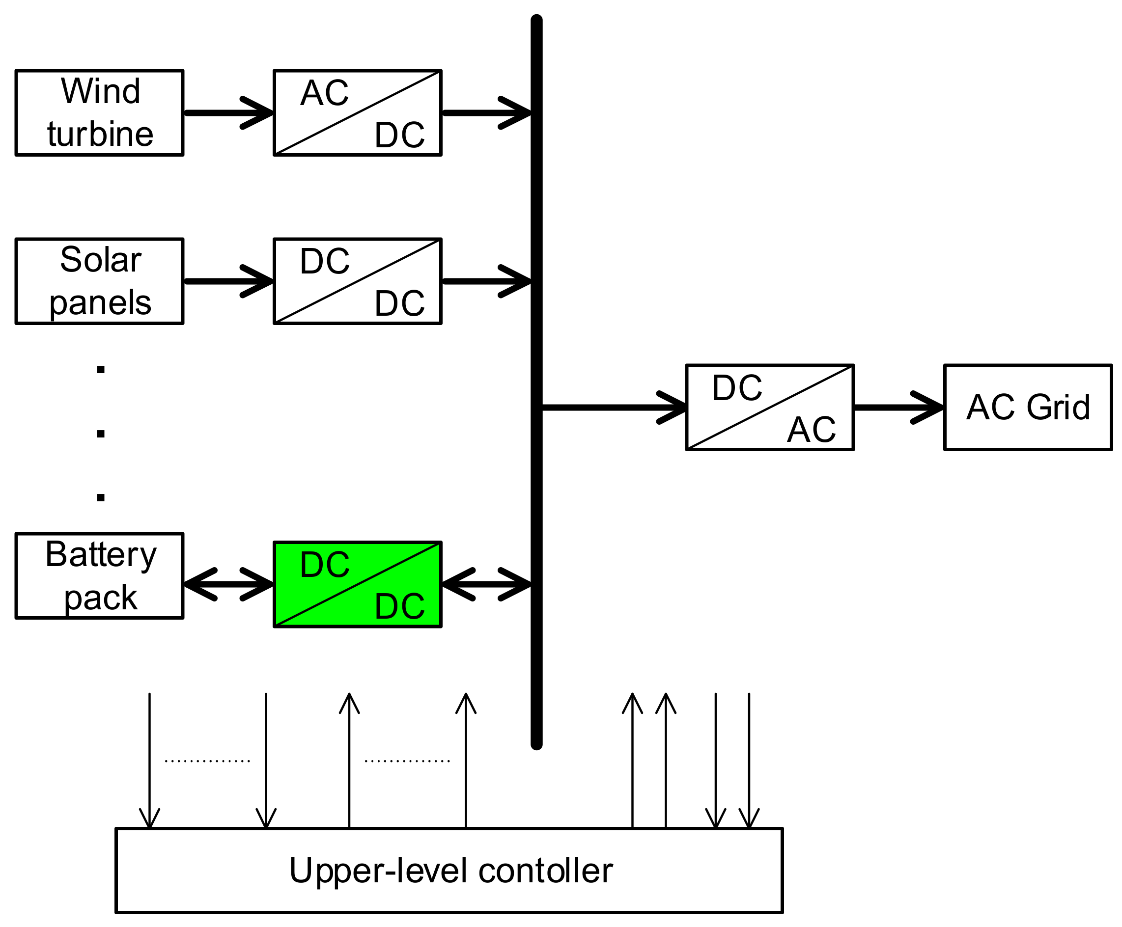
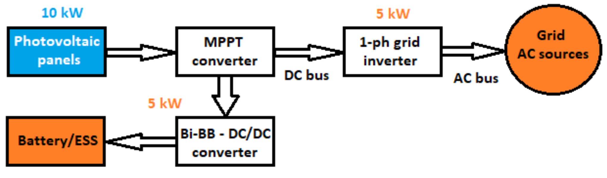
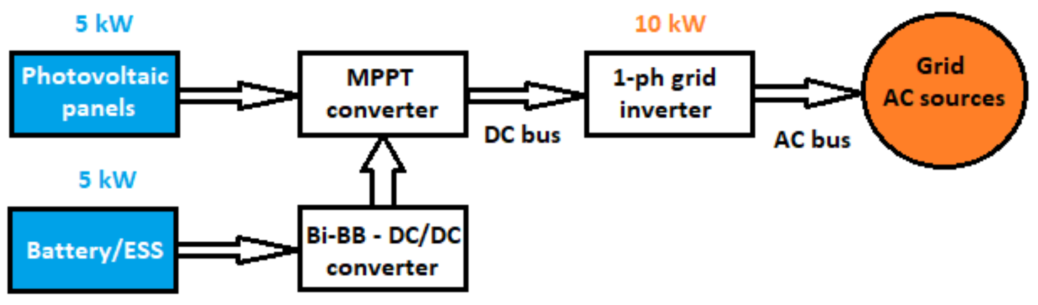
2. Description of Considered Microgrid Concept

A principal block diagram of the proposed microgrid is shown in Figure 2. The block diagram is proposed for the standard installation of PV panels and an energy storage system of the household, which reflects a power level of approximately 10 kW. The presented concept consist of the following main functional blocks:
  • Photovoltaic cells;
  • MPPT DC-DC converter;
  • Energy management block;
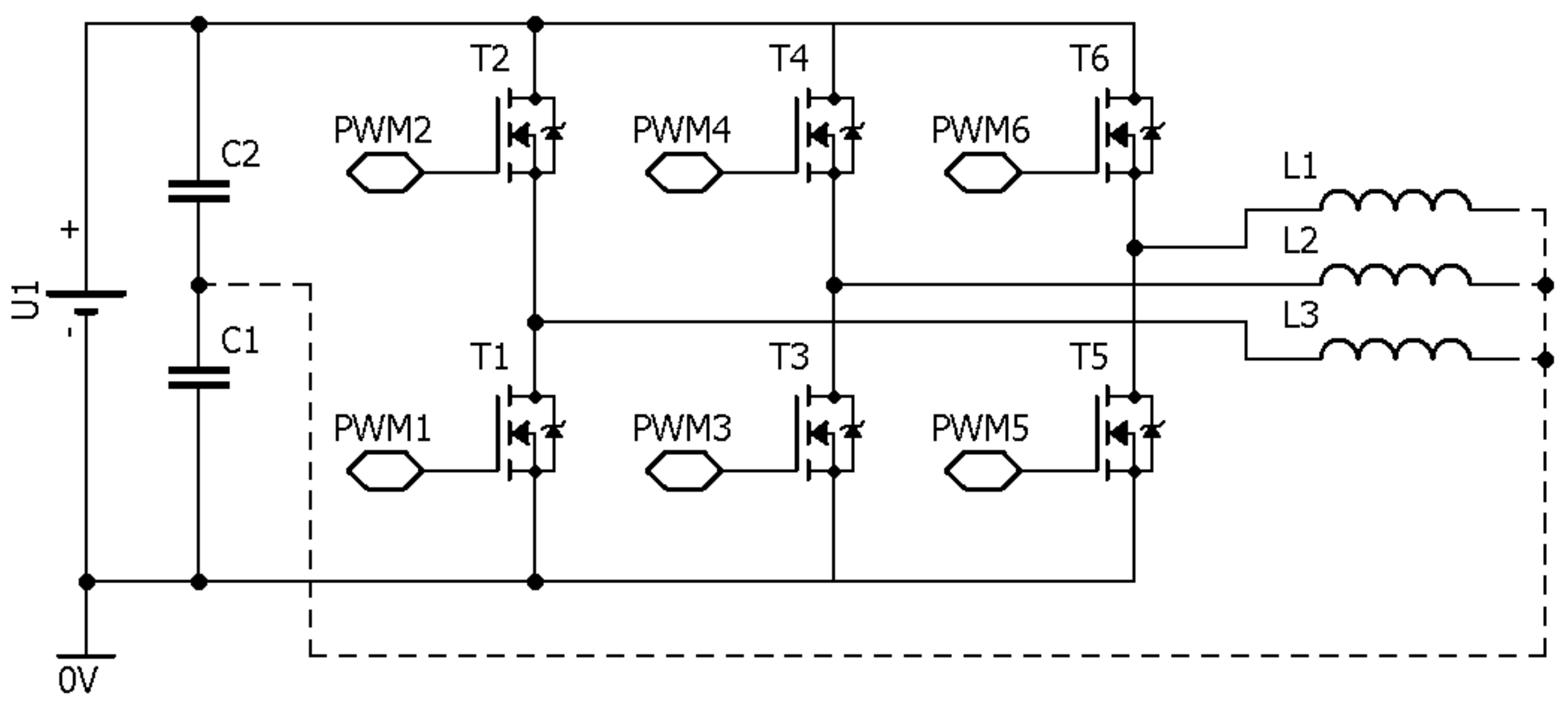
  • One-phase inverter;
  • Energy storage block;
  • Bidirectional DC-DC converter for energy flow control from and into the energy storage system;
  • Control and communication block.
The converters, which are used for the investigation of accuracy comparisons between experimental and simulation models, are an MPPT converter as well as a bidirectional buck/boost converter that are located between DC bus and energy storage elements [22,23,24]. Because of the laboratory conditions, the ratio of the input to output parameters is 1:10 as compared with a real system. In the next section, we describe the evaluation of the properties of individual power converter alternatives.

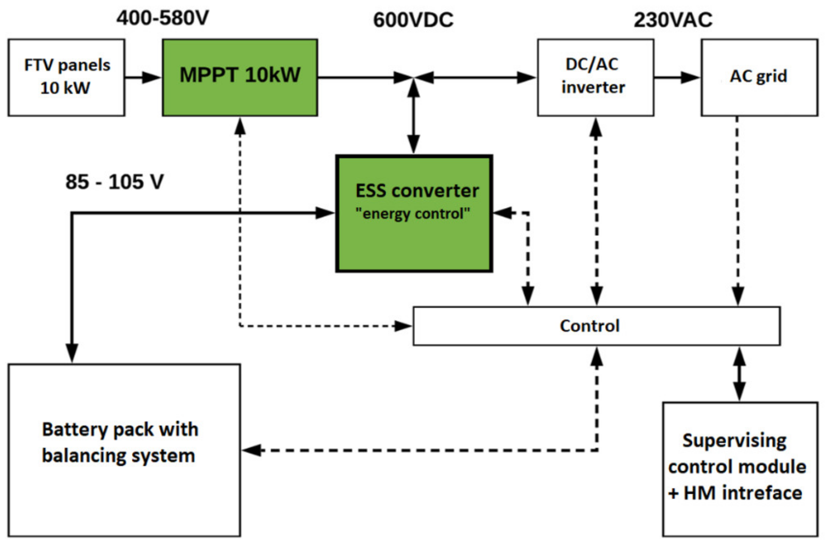
2.1. Circuit Alternatives of Microgrid Individual Power Electronic Converters

2.1.1. Maximum Power Point Tracking (MPPT) Converter Solution

The main task of the MPPT converter within the proposed microgrid is to convert the fluctuating DC voltage obtained from photovoltaic panels to a stable DC voltage. The MPPT algorithm, i.e., the algorithm for achieving the highest possible panel performance, is implemented in the inverter control system if HIL is considered. The most common and simplest solution for the mentioned application is a traditional boost converter, which, in addition to its simple design, also provides very high efficiency (with a synchronous rectifier of up to 99%). For higher outputs (of the order of kW, MW), the structure can be supplemented by other identical converters (1 to n), and then the individual converters work with a phase shift (interleaved). By using an interleaved topology, we obtain lower output voltage ripple, lower input current ripple, and a smaller overall drive volume, but at the cost of design complexity, more complex control, and potentially higher costs [23].
Figure 3 depicts an improved dual interleaved converter by implementation of flux reset circuitry within the main topology [19,20,21]. It consists of additional inductance and output diodes. All three inductors must be wound on one magnetic core. The PWM signals are phase shifted by 180° and the pulse width range can be from 0% to 90% (dependent on the inductor construction). The inverter achieves a high voltage gain (higher than a traditional boost converter) with high efficiency (up to 96%). In addition, the voltage gain can also be changed by the ratio of the turns (inductances) of the coupled inductor, while it must be valid that N1 = N2 : N3. A detailed study regarding this topic is available in [25,26,27].
Table 1 shows that the improved dual interleaved converter has the best efficiency as compared with the individual alternatives, even the number of semiconductor switches is doubled. The improvement in efficiency is related to the type of magnetic component used, i.e., the improved converter uses a much lower magnetic core and utilizes a reset winding that eliminates saturation of the core as compared with the alternative solutions. Due to the low output voltage ripple, the output electrolytic capacitors can be reduced, i.e., their value is much lower as compared with standard topologies. In this way, the optimization results in the reduction of ESR (Equivalent Series Resistance), and thus other losses. A second issue related to efficiency improvement is the benefit of the proposed magnetic design of the inductor due to the fact that it operates as a rigid voltage transformer with the given transformer ratio (coupling coefficient must be very high).

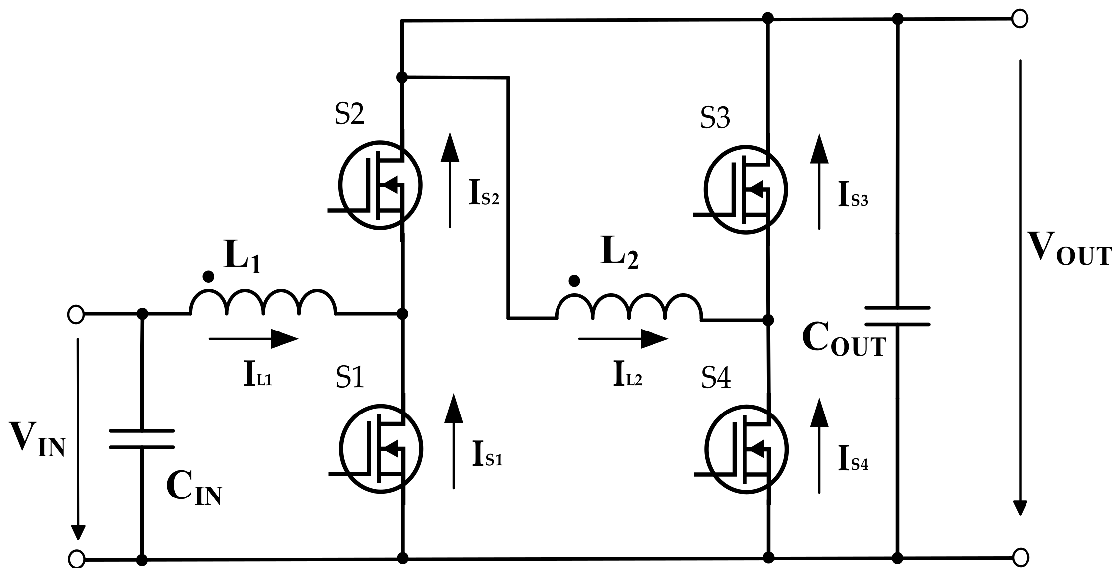
2.1.2. Bidirectional DC-DC Converter for Energy Flow Control

This subsystem of the considered microgrid provides a bidirectional interface between the DC link and the energy storage system (ESS). It provides charging/discharging of the batteries depending on the selected power delivery or based on a predefined battery state of charge control. The principle of the operation is simple and is based on using a traditional step-up converter with a synchronous rectifier. The modified circuit enables bidirectional energy transmission and its correct operation is already the task of a suitable control circuit. The converter has excellent efficiency (up to 98%), but its use is possible only in the case where galvanic isolation between the primary and secondary part of the circuit is not required. If high power operation is required (~10 kW) an interleaved solution is preferred [28,29].
For the purposes of the analyses of the considered DC smart grid concept using HIL and in relation to the design of the microgrid´s ESS power converter system, the focus is on an evaluation of the properties of a dual interleaved bidirectional buck-boost (Bi-BB) converter as the non-modular topology (Figure 4).

2.1.3. Alternatives for DC Link and AC Grid

The interface between the DC microgrid and the AC distribution grid is represented by a three-phase inverter (Figure 5). It ensures the flow of produced energy from the DC microgrid towards the AC distribution system, depending on the selected energy flow control plan. The inverter’s control system should allow the compensation of reactive power components so that the production of quality energy is achieved with the lowest possible content of harmonics and other interfering signals. A conventional full-bridge inverter has been selected for the DC/AC inverter part, which provides enough parameters for the use within considered application.

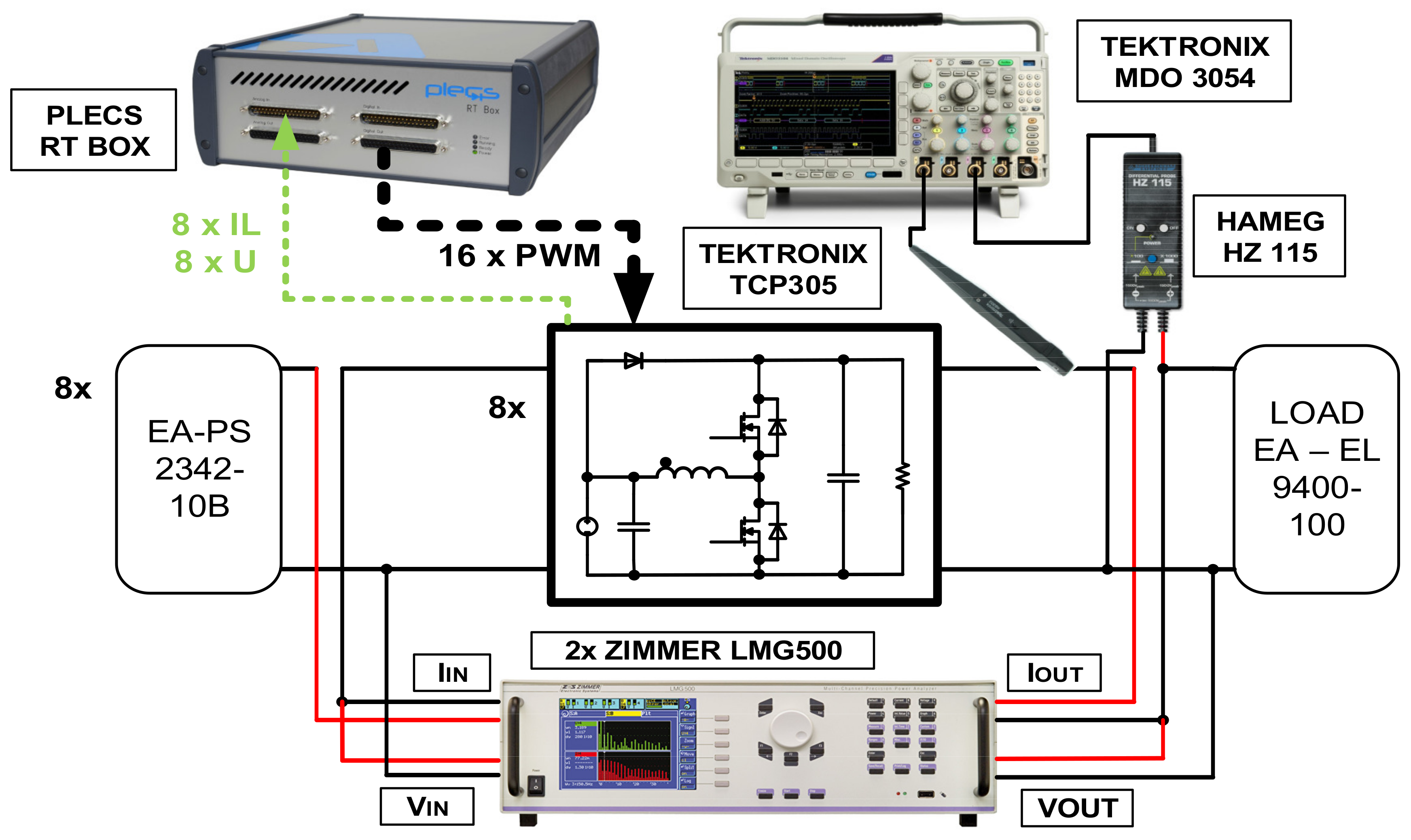
3. Evaluation of the Accuracy of the Hardware-in-the-Loop (HIL) Simulation Models

At this point, the focus is on the evaluation of the individual converter´s simulation models, while the maximum power point tracking (MPPT) converter is modeled as a dual interleaved boost with magnetic flux reset circuitry. Secondly, the bidirectional converter is also evaluated; here, a nonmodular dual interleaved bidirectional converter is considered. The accuracy of the proposed simulation approach is verified through experimental measurements, whereby the relative error is calculated for the case of bidirectional converters.

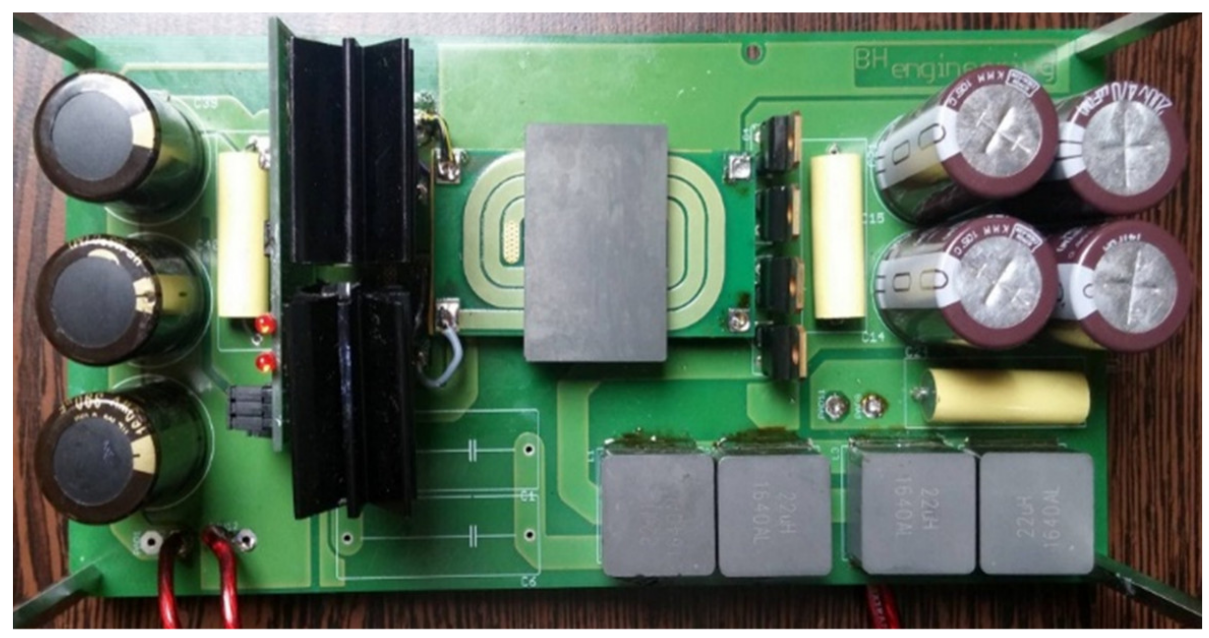
3.1. Evaluation of the MPPT Converter

For the first performance investigation between a simulation model (Figure 7) and an experimental sample (Figure 6), the perspective MPPT converter with coupled inductors and a flux reset circuit is evaluated. As previously mentioned, each converter of the proposed DC-microgrid concept is modeled in a PLECS simulation. To increase the accuracy of the simulations, the thermal and magnetic domains are defined for each model. Instead, the selected semiconductors of the converter prototypes have been modeled using their loss models (Figure 7). With this approach, it is possible to achieve accurate behavior of the circuit schematics which are modeled within a linearized approach [30,31]. The input to output parameters of the physical sample of MPPT converter are as follows (these parameters have also been defined for the simulation model):
-
VIN = 100 V;
-
Switching frequency (fSW) = 100 kHz;
-
POUT = 1 kW (2.5 A);
-
Duty cycle = D1 = D2 = 0.4;
-
Voltage gain = 3.6 (N1 = N2 = 6, N3 = 10 => TR = 1:1.7).
As shown in Figure 7, the designed model also uses the MPPT algorithm control together with models of photovoltaic panels. Here, it must be noted that this concept is also utilized within HIL, while for the investigation of the model’s performance, the input part of converter was replaced by a DC input source, as in laboratory experiments [28].
Figure 8 shows the waveforms received from experimental measurements of the proposed converter. The focus was on the waveforms of the coupled inductor and magnetic flux reset circuit. For each coil, the waveforms of currents and voltages are depicted for one switching cycle at nominal load and steady-state operation.
Figure 9 shows the results from the simulation experiments. Similarly, previous situation waveforms for inductor currents and voltages are analyzed. By comparing those results, it is seen that the shapes and character of voltages and currents within the inductors are the same as for the experimental measurements. Therefore, the simulation model’s suitability is effective for the HIL modeling purposes. The results support that magnetic modeling, together with proper thermal models of the semiconductors, offers high accurate results.

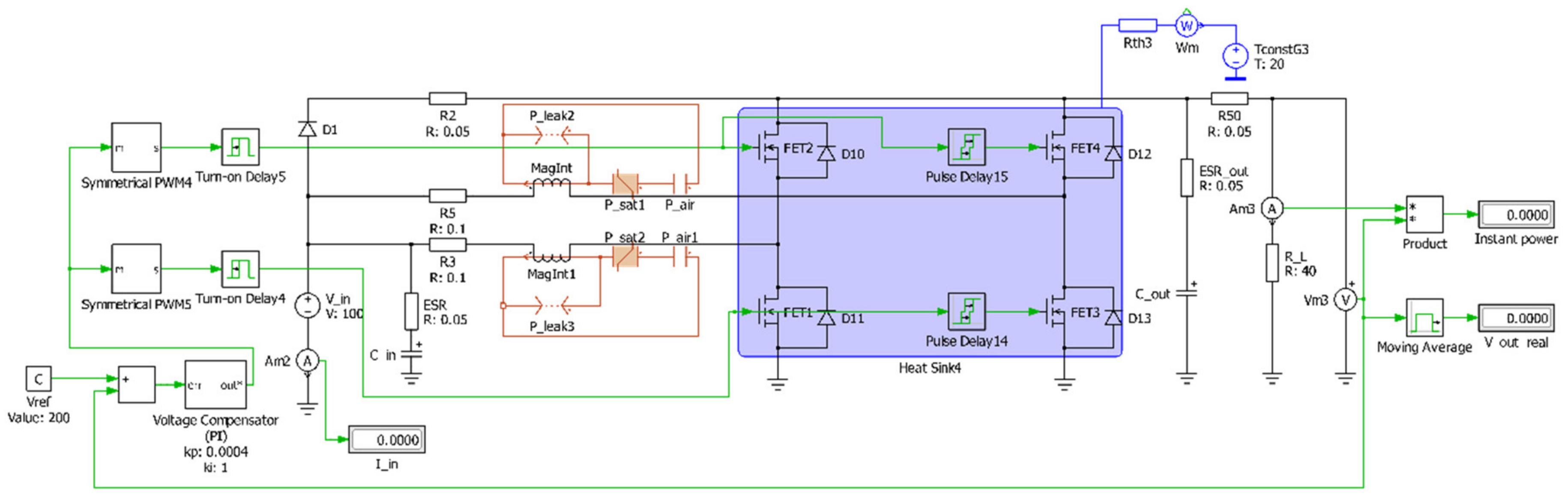
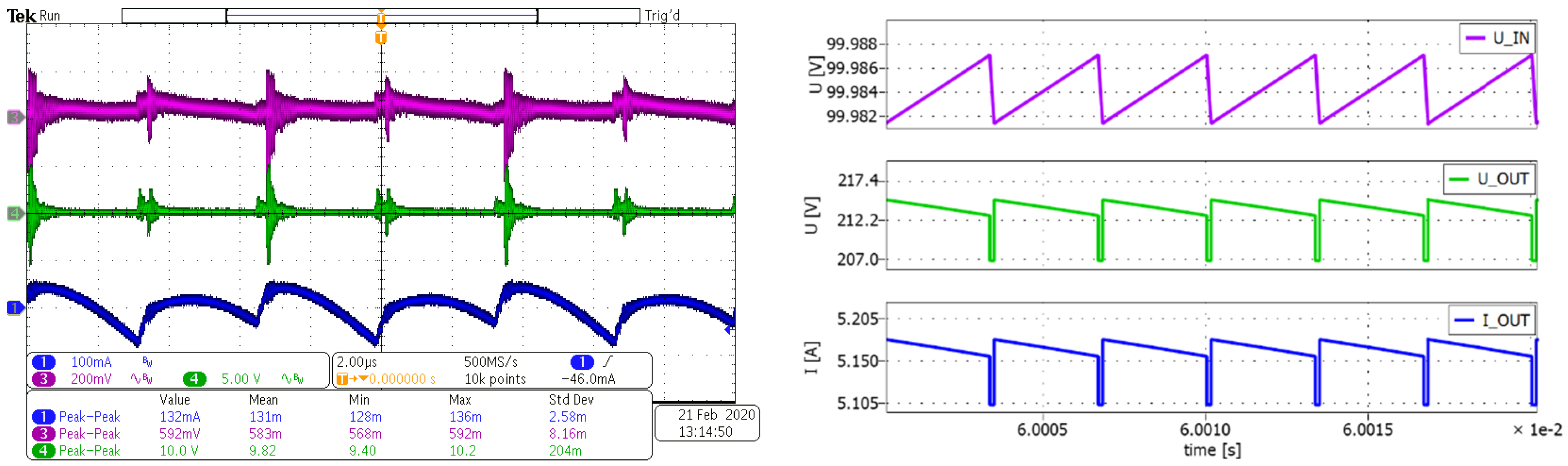
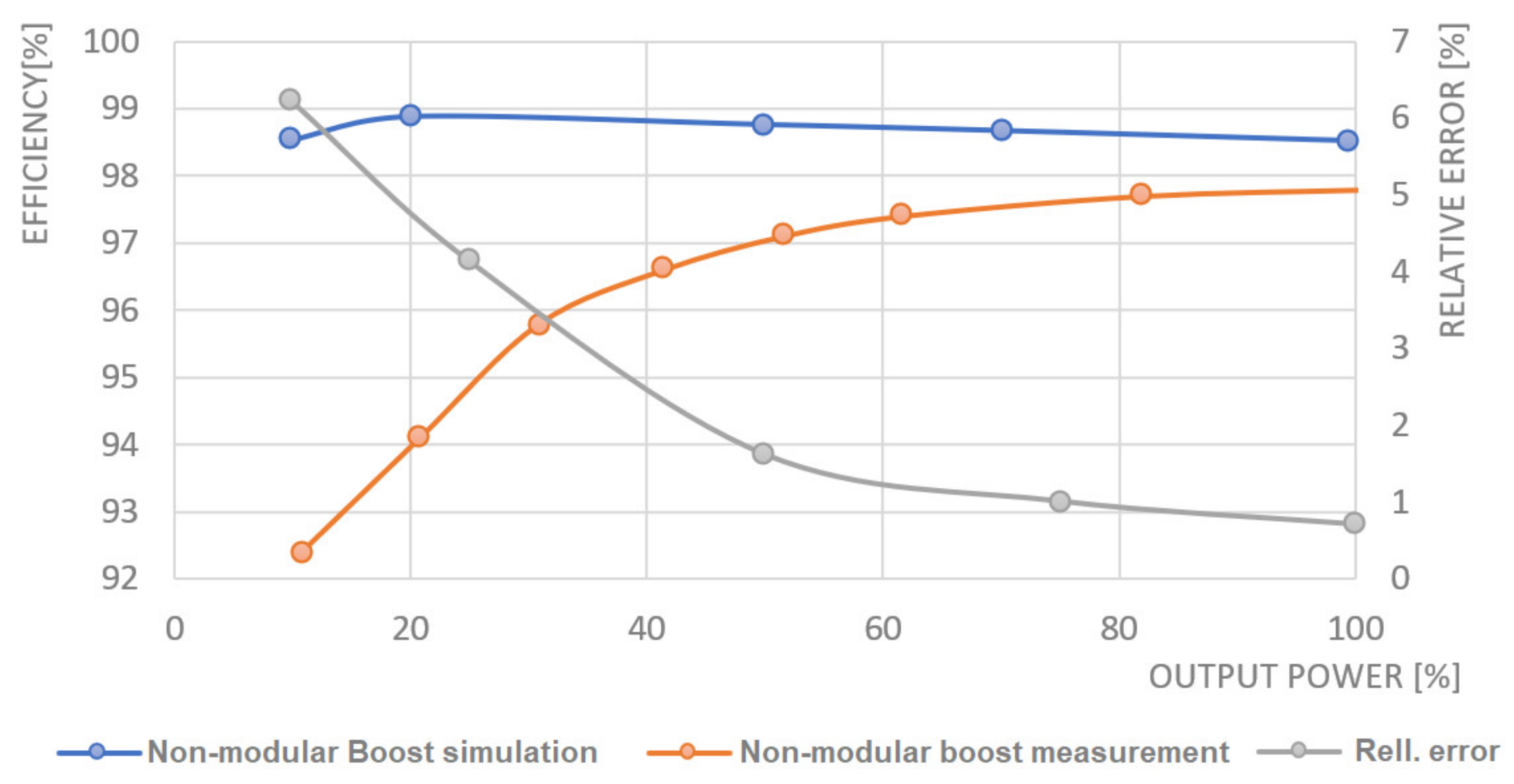
3.2. Evaluation of the Energy Flow Control Converter

The main circuit specifics for the non-modular solution are listed below. The proposed Bi-BB converter is based on SiC transistors technology and operates at 150 kHz of switching frequency as follows:
-
VIN = 100 V (boost mode), 200 V (buck mode);
-
Switching frequency (fSW) = 100 kHz (non-modular;,
-
VOUT = 200 V (boost mode), 100 V (buck mode);
-
POUT = 1 kW.
Figure 10 shows a physical sample of the proposed Bi-BB converter. The non-modular concept uses inductors that are made on PQ40 N87 cores, while winding is made of isolated copper foil in order to achieve low conduction losses. To secure the safety of control system and PWM generator, together with other system components, the isolation on the side of gate drivers is used.
First, the non-modular solution is evaluated. The simulation model used for the verification of the operation is shown in Figure 11. The thermal performance together with magnetic components modeling are designed according to parameters of the physical sample. In addition, the semiconductor devices use exact data of the losses received from manufacturer’s datasheets, while the main circuit also contains parasitic components (resistances and inductances of printed circuit board (PCB) traces, leads, etc.) [32].
Figure 12 shows the comparisons of operational waveforms of the non-modular Bi-BB converter and the experimental measurements and simulation results, while nominal power was considered. The data generated from the oscilloscope show inductor currents, while the AC coupling was adjusted. The converter operates in continuous conduction mode. The simulation result shows similar waveforms; thus, inductor currents are evaluated. It can be observed that, when the converter operates under continuous conduction mode (CCM) conditions, if the experiments are compared, the amplitudes (peak to peak) and character of currents are the same.
Figure 13 shows the time waveforms of the input and output ripples of the voltages and currents. Here, input voltage fluctuation for full load is evaluated, together with output voltage and current ripple. The results show that the simulation model was effectively optimized as it exhibited similar behavior to the experimental sample, i.e., voltage ripple at the input is about 100 mV for the experimental sample, while 60 mV for the simulation, etc.
As was previously mentioned, an additional evaluation of simulation model accuracy was conducted by comparing the efficiency characteristics of the Bi-BB converter operated in boost and buck modes. Because the experimental evaluation of efficiency is a complex task, it requires expensive laboratory equipment. The details of the experimental set-up for the measurements are shown in Figure 14.
Figure 15, Figure 16, Figure 17 and Figure 18 show comparisons between the simulation and measurement sample for evaluating the efficiency parameter and, consequently, the relative error is identified.
The buck and boost modes of operation were both tested. The experiment was conducted for a wide range of output power of the converter, i.e., within 10–100% of the power.
Figure 15 shows the comparison of the efficiency characteristic for the boost model of operation together with the evaluation of relative error for each power level. The results indicate that the simulation model exhibits lower accuracy for the power loads from 10% up to 50%, while the error is within 6–2.5%. Above 50% of the power load, the relative error drops to approximately 1% up to 100% of power.
Figure 16 shows the efficiency comparison between the simulation and measurement samples, while the proposed Bi-BB converter was operated in buck mode. Here, the evaluation of relative error was also realized for the total spectrum of output power. The results are similar to the previous experiment, i.e., the values of relative error vary between 2.5% and 7% up to 50% of the output power, while above this value, the relative error drops to approximately 1% for full power load.
The relative error of the efficiency characteristics for both modes of operation ranged from 0 to 7%. The relative deviations of the simulation and experimental results are caused by various parasitic parameters that influenced the physical samples of the converter. These parasites are, for example, DC resistances of component leads, DC resistances of printed circuit boards, resistances of magnetic components, parasitic capacitances of PCB and used components, etc. Most of these components exhibit high thermal dependency, i.e., the values change based on the temperature variation. These effects cannot be simply included within the proposed model, because the level of complexity increases significantly, and therefore is not appropriate for HIL modeling. Another possible source of deviation can be the piecewise linear electric circuit simulator (PLECS) simulation software, which uses simplified linearized component models to simplify and speed up calculations. This means that it is possible to increase the speed at the cost of accuracy reduction. In the case of a physical sample of a non-modular solution, there are several unfavorable factors, such as the use of PCBs with a thin thickness of copper layer, as well as suboptimal implementation of coils that had a low number of turns which causes saturation at full load of the converter. It was not possible to wind many turns on the core due to the thickness of the copper foil. If an optimal coil design is used, the efficiency of the converter could be increased, especially in the power load range of 0–50%.

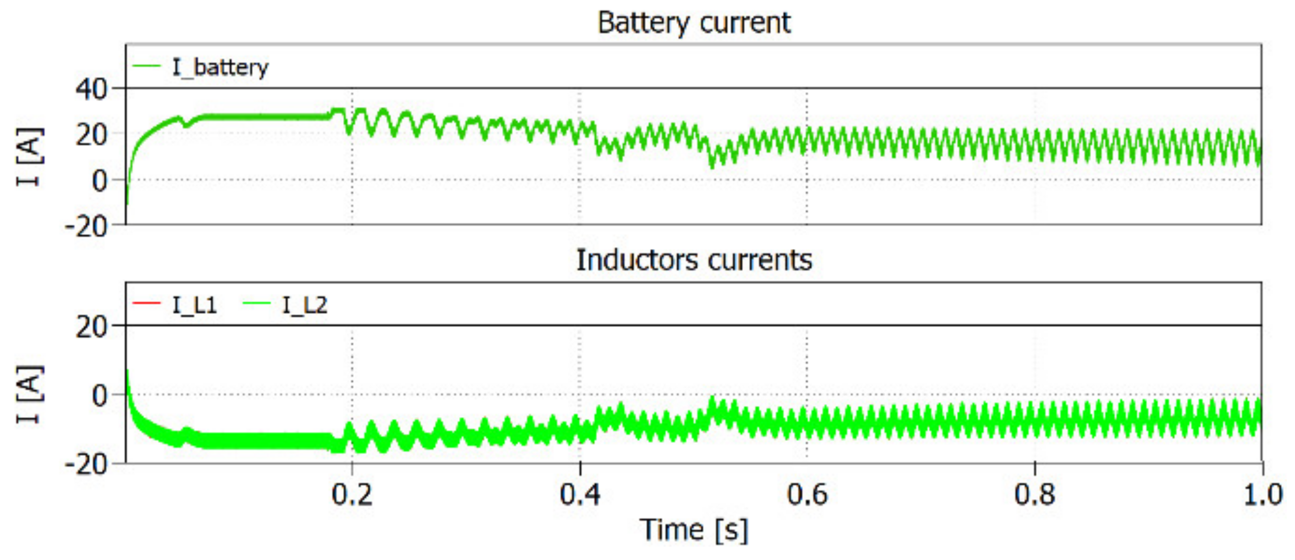
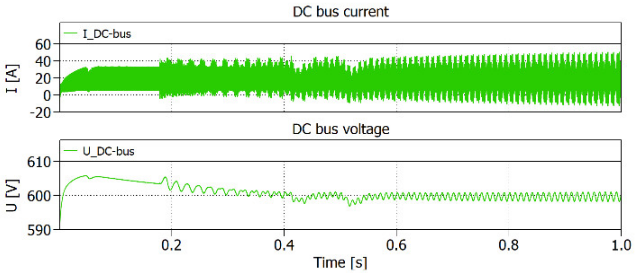
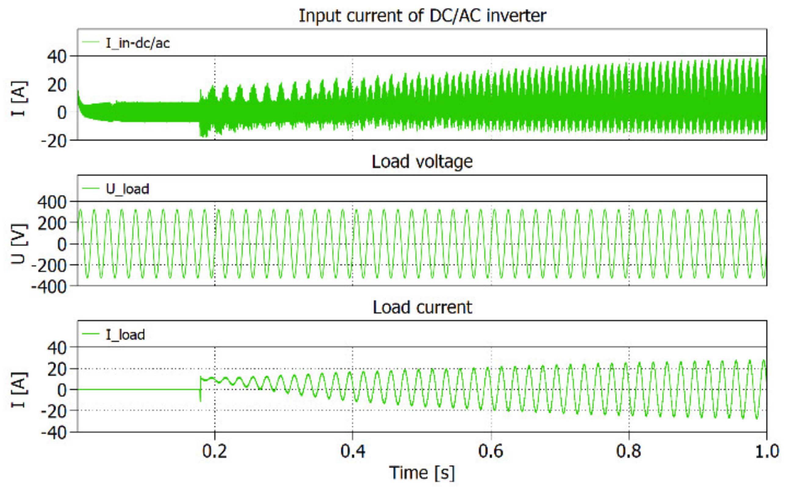
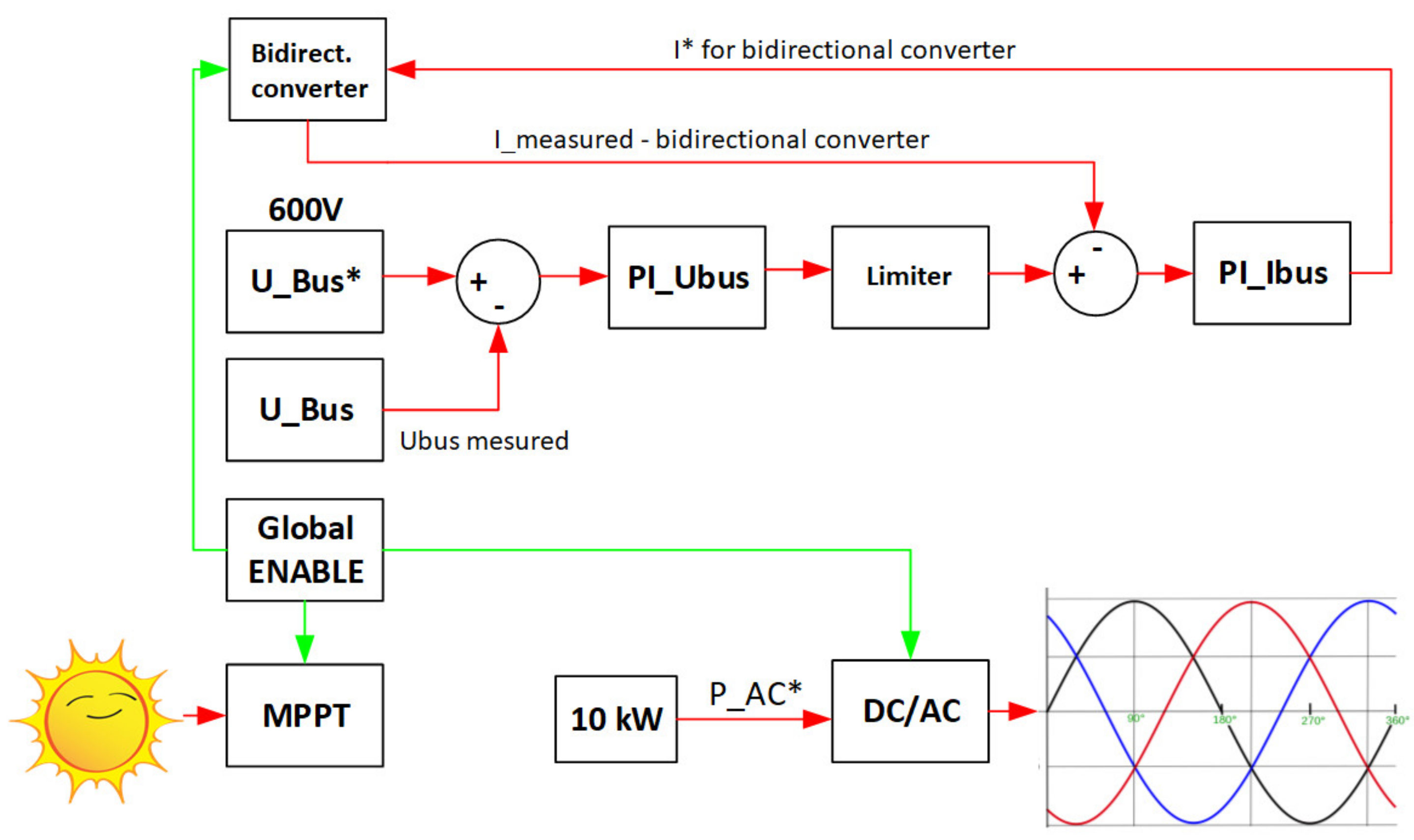
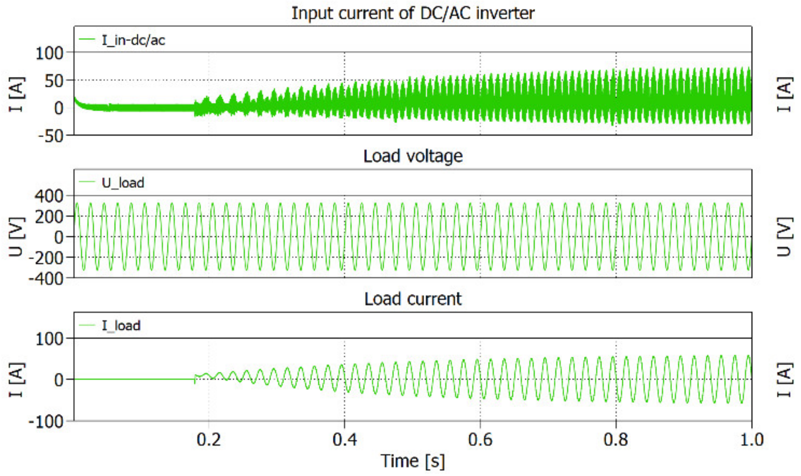
4. HIL of the Proposed Smart Grid Concept and the Test of Possible Operational Scenarios

After experimental verification of the parameters of the constructed physical samples of converters, a simulation analysis of the complex microgrid system (Figure 2) within the PLECS simulation software was constructed. The simulation parameters of the individual power converters were adjusted according to the real microgrid system to ensure the highest possible substantiality, i.e., each of the verified converters was reconfigured for higher power (10 kW of the peak operation).
The main contribution of the presented approach is to show the advantages of a piecewise linear electric circuit simulator for modeling of complex power semiconductor systems. Previously, it was shown that with the use of relevant magnetic and thermal domains, satisfactory accuracy of simulation models could be achieved. Therefore, next, the presented approach is validated through a simulation of microgrid operation. To investigate the behavior of the proposed microgrid concept, two operational scenarios were proposed, and are described in Section 4.1 and Section 4.2.

4.1. Operational Scenario 1

The first operational scenario is graphically depicted in Figure 17. Considering a photovoltaic energy source, 100% of the sunlight is initially assumed, thus, full power (10 kW) is being supplied. The MPPT converter supplied DC variables to DC bus (Figure 17), while half of the power was supplied to the grid inverter (requirement from consumer) and the second half of the power was transferred through the Bi-BB converter into the energy storage system (full capacity 40 kWh initially charged at 50% of full capacity). In this case, there are no dynamic changes at the inputs or outputs. The principle of the operation of the supervising control system modeled within PLECS is described in Figure 18 for Scenario 1.
The requirement for a DC/AC inverter (5 kW) is half of the energy converted by the photovoltaic panels. The setpoint for the DC bus voltage of the microgrid is 600 V. This value is compared with the actual value and enters the voltage regulator (Figure 18). Next, there is a reference current limiter, from where the signal is compared with the actual value and continues to the current regulator for the bidirectional converter. The “Global ENABLE” signal is also fed to all subordinate control systems, which evaluates the voltage and undervoltage of the DC microgrid, and in the case of exceeding any limit, the entire system is switched off [33].
Figure 19, Figure 20 and Figure 21 show the main operational variables of the investigated DC microgrid, i.e., ESS current, DC bus voltage, and DC bus sourced current feeding the grid inverter, which is represented by AC grid voltage and the current. The evaluation of the qualitative indicators of the DC microgrid concept, for example, efficiency, power factor, voltage, and current ripples, is listed in Table 2. It can be seen that, for this operational scenario, the system efficiency reaches 54%. This result is highly affected by the power loading of the grid inverter, in addition, total harmonic distortion of the grid current reaches 4.3%. It must be noted that the experiments have been provided for resistive-inductive load. Therefore, it could be assumed that the proposed model should be further improved through the investigation of the various types of loads within the AC grid, including the influence of power factor correction circuits.

4.2. Operational Scenario 2

For the second operational scenario (Figure 22), it is assumed that 50% of the available power is sourced from the MPPT converter and photovoltaic panels into the AC grid. The remaining power required by the grid is supplied from the energy storage system. In summary, 5 kW is supplied by renewable sources and 5 kW by energy storage system, and thus 10 kW are sourced within the supply grid. The principle of the operation of the supervising control system modeled within PLECS is illustrated in Figure 23 for Scenario 2.
The requirement for a DC/AC inverter is 10 kW. The setpoint for the DC bus voltage of the microgrid is again 600 V. This value is compared with the actual value and enters the voltage regulator (Figure 23). Next, there is a reference current limiter, from where the signal is compared with the actual value and continues to the current regulator for the bidirectional converter. The “Global ENABLE” signal is also fed to all subordinate control systems, which evaluates the voltage and undervoltage of the DC microgrid, and in the case of exceeding any limit, the entire system is switched off.
Figure 24, Figure 25 and Figure 26 show the main operational variables of the investigated DC microgrid, i.e., ESS current, bidirectional converter inductor currents, DC bus voltage, and DC bus sourced current feeding the grid inverter, which is represented by the AC grid voltage and current as well. The evaluation of the qualitative indicators of DC microgrid concept, for example, efficiency, power factor, voltage, and current ripples, is listed in Table 3. From the achieved results, it is seen, that system efficiency from source to the load reaches approximately 77% for this operational scenario. These results are better as compared with the results from Table 2. The results are influenced by the efficiency performance of the Bi-BB converter as well as by the efficiency of the MPPT converter, which operates at 50% of the power load. For that operational point, the efficiencies are lower as compared with full power of the converters. If the proper control algorithm regarding power sharing is used, the efficiency for the presented operation scenario could be improved, therefore, the proposed HIL model should allow us to identify the most proper operational point.

5. Discussion

In this paper, the procedure of the HIL modeling referred to as the power stage of the smart grid was discussed. The main focus was the development of high-precision simulation models of individual power converters belonging to an SG concept, while a piecewise linear electronic circuit simulator is used.
The main benefits of using a piecewise linear simulator are the possibility to model complex power electronic systems and to analyze their behavior as a real-time system within an acceptable simulation time. The presented approach considered the physical properties and processes which cannot be omitted if high accuracy of a simulation model as compared with a physical model is required. In this study, we consider thermal processes, magnetic properties, and nonlinear behavior of inductive components, or power semiconductor devices modeling. All the mentioned regularities were considered and confirmed by experimental comparisons. The results indicated that the simulation models of individual power semiconductor converters exhibited very high accuracy if real-time operation is considered, or efficiency evaluation is performed. Since the demands on calculations in such cases are significantly lower than in nonlinear systems, it is assumed that the presented procedure can reliably model complex power semiconductor systems such as a smart grid. The presented operating scenarios represent an introduction to a possible comprehensive investigation of the operation of SGs regarding the influence on qualitative indicators of a SG, if we consider the characteristics of power semiconductor converters. Our results should be considered in future studies, with the main focus of investigating the supervision control algorithms for targeting the highest efficient operation of DC microgrids.

6. Conclusions

On the basis of our results, we have confirmed that even with the use of linearized approximated models, high accuracy of simulation results can be achieved as compared with experimental measurements. We described our investigation in detail and the results were verified through a designed perspective dual interleaved converter with a demagnetization circuit and a dual interleaved buck/boost bidirectional converter; both converters were experimentally tested and analyzed. Consequently, simulation models of both converters were developed, and the circuit variables were compared to experimental waveforms. We found that the simulation models showed high accuracy considering operational waveforms. This achievement was also verified by comparing the efficiency performance of the experimental measurements and simulation. We found that, above 50% of nominal power, the relative error between the simulation and experimental measurements was lower than 1%.
We have proposed the design approach for modeling of a smart grid system. A characteristic feature in terms of modeling is the possibility of investigating the impact of the operating characteristics of individual semiconductor converters within the SG, and therefore it is also possible to investigate the influence of possible topological variations within the power stage of a SG. For example, in the analysis of SG operation, the main circuit variables are evaluated, as well as their ripples, and the efficiency of the energy system for a given operating scenario. The presented results are valid for a DC microgrid system with 10 kW of power capability. If systems with significantly higher power ratings are to be modeled, a possible limitation of the presented methodology is the lack of a simple verification method for simulation models with physical prototypes because of the lack of laboratory infrastructure and equipment for high-power level design and measurement.

Author Contributions

Supervision, conceptualization, methodology, writing—review and editing by M.F.; investigation and data curation by J.M.; validation and formal analysis by M.P.; original draft preparation by K.T. All authors have read and agreed to the published version of the manuscript.

Funding

This research was funded by Slovak National Grant Agency Vega for project support 1/0593/20.

Acknowledgments

The authors wish to thank the project funding from Slovak National Grant Agency Vega for project support 1/0593/20.

Conflicts of Interest

The authors declare no conflict of interest.

References

  1. Sallan, J.; Villa, J.L.; Llombart, A.; Sanz, J.F. Optimal Design of ICPT Systems Applied to Electric Vehicle Battery Charge. IEEE Trans. Ind. Electron. 2009, 56, 2140–2149. [Google Scholar] [CrossRef]
  2. Davison, M.J.; Summers, T.J.; Townsend, C.D. A review of the distributed generation landscape, key limitations of traditional microgrid concept and possible solution using an enhanced microgrid architecture. In Proceedings of the 2017 IEEE Southern Power Electronics Conference (SPEC), Puerto Varas, Chile, 4–7 December 2017; pp. 1–6. [Google Scholar] [CrossRef]
  3. AbdelGawad, H.; Sood, V.K. A Comprehensive Review on Microgrid Architectures for Distributed Generation. In Proceedings of the 2019 IEEE Electrical Power and Energy Conference (EPEC), Montreal, QC, Canada, 16–18 October 2019; pp. 1–8. [Google Scholar] [CrossRef]
  4. El Mariachet, J.; Guan, Y.; Matas, J.; Martín, H.; Li, M.; Guerrero, J.M. HIL-Assessed Fast and Accurate Single-Phase Power Calculation Algorithm for Voltage Source Inverters Supplying to High Total Demand Distortion Nonlinear Loads. Electronics 2020, 9, 1643. [Google Scholar] [CrossRef]
  5. Go, S.-I.; Choi, J.-H. Design and Dynamic Modelling of PV-Battery Hybrid Systems for Custom Electromagnetic Transient Simulation. Electronics 2020, 9, 1651. [Google Scholar] [CrossRef]
  6. Cacciato, M.; Consoli, A. New regenerative active snubber circuit for ZVS phase shift Full Bridge converter. In Proceedings of the 2011 Twenty-Sixth Annual IEEE Applied Power Electronics Conference and Exposition (APEC), Fort Worth, TX, USA, 6–11 March 2011; pp. 1507–1511. [Google Scholar]
  7. Kumar, G.V.B.; Palanisamy, K. A Review on Microgrids with Distributed Energy Resources. In Proceedings of the 2019 Innovations in Power and Advanced Computing Technologies (i-PACT), Vellore, India, 22–23 March 2019; pp. 1–6. [Google Scholar] [CrossRef]
  8. Tutak, M.; Brodny, J.; Siwiec, D.; Ulewicz, R.; Bindzár, P. Studying the Level of Sustainable Energy Development of the European Union Countries and Their Similarity Based on the Economic and Demographic Potential. Energies 2020, 13, 6643. [Google Scholar] [CrossRef]
  9. Lu, H.-F.; Lin, B.-L.; Campbell, D.E.; Sagisaka, M.; Ren, H. Interactions among energy consumption, economic development and greenhouse gas emissions in Japan after World War II. Renew. Sustain. Energy Rev. 2016, 54, 1060–1072. [Google Scholar] [CrossRef]
  10. Dogan, E.; Seker, F. Determinants of CO2 emissions in the European Union: The role of renewable and non-renewable energy. Renew. Energy 2016, 94, 429–439. [Google Scholar] [CrossRef]
  11. EU Climate Action and the European Green Deal. Available online: https://ec.europa.eu/clima/policies/eu-climate-action_en (accessed on 1 January 2021).
  12. Consoli, A.; Attanasio, R.; Cacciato, M.; Scarcella, G.; Gennaro, F.; Testa, A. A Novel Converter System for Fuel Cell Distributed Energy Generation. In Proceedings of the IEEE 36th Conference on Power Electronics Specialists, Recife, Brazil, 12–16 June 2005; pp. 1621–1627. [Google Scholar]
  13. Hruska, K.; Kindl, V.; Pechanek, R. Concept, design and coupled electro-thermal analysis of new hybrid drive vehicle for public transport. In Proceedings of the 14th International Power Electronics and Motion Control Conference EPE-PEMC 2010, Ohrid, Macedonia, 6–8 September 2010; pp. S4–S5. [Google Scholar]
  14. Frivaldsky, M.; Dobrucky, B.; Scelba, G.; Spanik, P.; Drgona, P. Bidirectional Step-Up/Step-Down DC-DC Converter with Magnetically Coupled Coils. Communications 2013, 15, 21–25. [Google Scholar]
  15. Yao, T.; Li, Z.; Qu, J.; Li, Z.; Zhao, Q.; Zhao, G. Research on Simplified Model of AC/DC Hybrid Microgrid for Fault Analysis. Electronics 2020, 9, 358. [Google Scholar] [CrossRef] [Green Version]
  16. Gupta, P.; Ansari, M. Analysis and Control of AC and Hybrid AC-DC Microgrid: A Review. In Proceedings of the 2019 2nd International Conference on Power Energy, Environment and Intelligent Control (PEEIC), Greater Noida, India, 18–19 October 2019; pp. 281–286. [Google Scholar] [CrossRef]
  17. Kondrath, N. Bidirectional DC-DC converter topologies and control strategies for interfacing energy storage systems in microgrids: An overview. In Proceedings of the 2017 IEEE International Conference on Smart Energy Grid Engineering (SEGE), Oshawa, ON, Canada, 14–17 August 2017; pp. 341–345. [Google Scholar] [CrossRef]
  18. Eid, B.M.; Rahim, N.A.; Selvaraj, J.; El Khateb, A.H. Control Methods and Objectives for Electronically Coupled Distributed Energy Resources in Microgrids: A Review. IEEE Syst. J. 2016, 10, 446–458. [Google Scholar] [CrossRef]
  19. Sparn, B.; Krishnamurthy, D.; Pratt, A.; Ruth, M.; Wu, H. Hardware-in-the-Loop (HIL) Simulations for Smart Grid Impact Studies. In Proceedings of the 2018 IEEE Power and Energy Society General Meeting (PESGM), Portland, OR, USA, 5–10 August 2018; pp. 1–5. [Google Scholar] [CrossRef]
  20. Nguyen, V.H.; Tran, Q.T.; Guillo-Sansano, E.; Kotsampopoulos, P.; Gavriluta, C.; Lauss, G.; Strasser, T.I.; Jensen, T.V.; Heussen, K.; Gehrke, O.; et al. Hardware-in-the-Loop Assessment Methods. In European Guide to Power System Testing; Strasser, T., de Jong, E., Sosnina, M., Eds.; Springer International Publishing: Cham, Switzerland, 2020; pp. 51–66. [Google Scholar] [CrossRef]
  21. Steinbrink, C.; Lehnhoff, S.; Rohjans, S.; Strasser, T.I.; Widl, E.; Moyo, C.; Lauss, G.; Lehfuss, F.; Faschang, M.; Palensky, P.; et al. Simulation-Based Validation of Smart Grids—Status Quo and Future Research Trends. In Constructive Side-Channel Analysis and Secure Design; Mařík, V., Wahlster, W., Strasser, T., Kadera, P., Eds.; Springer International Publishing: Cham, Switzerland, 2017; Volume 10444, pp. 171–185. [Google Scholar] [CrossRef] [Green Version]
  22. Ebe, F.; Idlbi, B.; Stakic, D.E.; Chen, S.; Kondzialka, C.; Casel, M.; Heilscher, G.; Seitl, C.; Bründlinger, R.; Strasser, T.I. Comparison of Power Hardware-in-the-Loop Approaches for the Testing of Smart Grid Controls. Energies 2018, 11, 3381. [Google Scholar] [CrossRef] [Green Version]
  23. Lauss, G.F.; Faruque, M.O.; Schoder, K.; Dufour, C.; Viehweider, A.; Langston, J. Characteristics and Design of Power Hardware-in-the-Loop Simulations for Electrical Power Systems. IEEE Trans. Ind. Electron. 2016, 63, 406–417. [Google Scholar] [CrossRef]
  24. Lundstrom, B.; Chakraborty, S.; Lauss, G.; Brundlinger, R.; Conklin, R. Evaluation of system-integrated smart grid devices using software- and hardware-in-the-loop. In Proceedings of the 2016 IEEE Power and Energy Society Innovative Smart Grid Technologies Conference (ISGT), Minneapolis, MN, USA, 6–9 September 2016; pp. 1–5. [Google Scholar]
  25. Frivaldsky, M.; Morgos, J. DC-DC Converter Design Issues for High-Efficient DC Microgrid. Commun. Sci. Lett. Univ. Zilina 2019, 21, 35–41. [Google Scholar] [CrossRef]
  26. Gabe, I.J.; Fabio, F.; Palha, K.; Pinheiro, H. Grid connected voltage source inverter control during voltage dips. In Proceedings of the 2009 35th Annual Conference of IEEE Industrial Electronics, Porto, Portugal, 3–5 November 2009; pp. 4571–4576. [Google Scholar] [CrossRef]
  27. Frivaldsky, M.; Hanko, B.; Prazenica, M.; Morgos, J. High Gain Boost Interleaved Converters with Coupled Inductors and with Demagnetizing Circuits. Energies 2018, 11, 130. [Google Scholar] [CrossRef] [Green Version]
  28. Aiello, G.; Cacciato, M.; Messina, S.; Torrisi, M. A High Efficiency Interleaved PFC Front- End Converter for EV Battery Charger. Communications 2018, 20, 86–91. [Google Scholar]
  29. Frivaldsky, M.; Kascak, S.; Morgos, J.; Prazenica, M. From Non-Modular to Modular Concept of Bidirectional Buck/Boost Converter for Microgrid Applications. Energies 2020, 13, 3287. [Google Scholar] [CrossRef]
  30. Turzynski, M.; Chrzan, P.J. Behavioural model of IGBT transistor. Przeglad Elektrotechniczny 2010, 86, 87–94. [Google Scholar]
  31. Turzyński, M.; Banach, P.; Murawski, P.; Peplinski, R.; Chrzan, P. A predictive estimation based control strategy for a quasi-resonant dc-link inverter. Bull. Pol. Acad. Sci. Tech. Sci. 2013, 61, 757–762. [Google Scholar] [CrossRef] [Green Version]
  32. Hruska, K.; Kindl, V.; Pechanek, R. Design and FEM Analyses of an Electrically Excited Automotive Syn-chronous Motor. In Proceedings of the 15th International Power Electronics and Motion Control Conference and Exposition (EPE-PEMC ECCE Europe), Novi Sad, Serbia, 4–6 September 2012. [Google Scholar]
  33. Drgona, P.; Prikopova, A.; Frivaldsky, M.; Priecinsky, M. Simulation Based Method for Design and Application of Digital Control System. Communications 2011, 13, 32–37. [Google Scholar]
Figure 1. Example of smart household utilizing various energy storage elements and sources.
Electronics 10 00644 g001
Figure 2. Block diagram of proposed microgrid for households.
Electronics 10 00644 g002
Figure 3. Circuit diagram of perspective dual interleaved boost converter with magnetic flux reset circuitry.
Electronics 10 00644 g003
Figure 4. Circuit schematic of non-modular interleaved bidirectional buck-boost (Bi-BB) converter.
Electronics 10 00644 g004
Figure 5. Circuit schematic of three-phase DC/AC inverter.
Electronics 10 00644 g005
Figure 6. Experimental prototype of perspective MPPT converter.
Electronics 10 00644 g006
Figure 7. Simulation model of perspective MPPT converter.
Electronics 10 00644 g007
Figure 8. Time waveforms received from experimental measurements of the MPPT converter. (left) Waveforms of the inductor’s currents; (right) Waveforms of the inductor’s voltages.
Electronics 10 00644 g008
Figure 9. Time waveforms received from the simulation experiments of the MPPT converter. (left) Waveforms of the inductor’s currents; (right) Waveforms of the inductor’s voltages.
Electronics 10 00644 g009
Figure 10. Experimental prototype of the non-modular bidirectional converter.
Electronics 10 00644 g010
Figure 11. Circuit schematic of the non-modular interleaved Bi-BB converter.
Electronics 10 00644 g011
Figure 12. Time waveforms of inductor currents (violet and green) and gate drive impulse (blue) of the non-modular Bi-BB converter for the experimental measurement sample (left) and simulation (right), in boost mode.
Electronics 10 00644 g012
Figure 13. Time waveforms of input voltage ripple (violet), output voltage ripple (green), and output current ripple of the non-modular Bi-BB converter for experimental measurement sample (left) and simulation (right) in boost mode.
Electronics 10 00644 g013
Figure 14. Block diagram of the principal configuration of the experimental test set-up during the evaluation of the efficiency characteristic for the Bi-BB converter.
Electronics 10 00644 g014
Figure 15. Comparison of efficiency characteristics for the simulation (blue) and the measurement (orange) samples and the evaluation of relative error between results in boost mode.
Electronics 10 00644 g015
Figure 16. Comparison of efficiency characteristic for simulation (blue) and measurement (orange) results and evaluation of the relative error between results at buck mode.
Electronics 10 00644 g016
Figure 17. Representation of the operational Scenario 1.
Electronics 10 00644 g017
Figure 18. Block diagram of supervising control system applied during Scenario 1.
Electronics 10 00644 g018
Figure 19. Battery and Bi-BB converter inductor currents for Scenario 1.
Electronics 10 00644 g019
Figure 20. Current and voltage of DC bus for Scenario 1.
Electronics 10 00644 g020
Figure 21. Current and voltage of grid load for Scenario 1.
Electronics 10 00644 g021
Figure 22. Representation of the operational Scenario 2.
Electronics 10 00644 g022
Figure 23. Block diagram of supervising control system applied during Scenario 2.
Electronics 10 00644 g023
Figure 24. Battery and Bi-BB converter inductor currents for Scenario 2.
Electronics 10 00644 g024
Figure 25. Current and voltage of the DC bus for Scenario 2.
Electronics 10 00644 g025
Figure 26. Current and voltage of the grid load for Scenario 2.
Electronics 10 00644 g026
Table 1. Performance comparison of individual converter solutions of the maximum power point tracking (MPPT) block.
Improved DIB
Converter
DIB ConverterBoost Converter
Output power500 W500 W500 W
Output voltage ripple19 mV180 mV364 mV
Input ripple current4.4 A17 A14 A
Output capacitor66 uF470 uF470 uF
Inductor VolumesE 43 PLTE50/27/15ETD59
Efficiency Pout = 100%96.7%91%90%
Maximum achievable voltage gain1:6 (valid for n = 1,6)
Note: can be increase through
turn ratio increase
1:191:10
Table 2. Evaluation of the operational variables of the proposed DC microgrid during Scenario 1.
VariableValues
UBUS (V)600.06
ΔUBUS (V)0.028
IL (A)8.2
ΔIL (A)3.12
UGRID (V RMS)230
PF (-)0.99
System efficiency (%)53.88
THD (-)4.3
Table 3. Evaluation of the operational variables of the proposed DC microgrid during Scenario 2.
VariableValues
UBUS (V)600.029
ΔUBUS (V)1.26
IL (A)7.15
ΔIL (A)3.1
UGRID (V RMS)230
PF (-)0.99
System efficiency (%)76.79
THD (-)3
Publisher’s Note: MDPI stays neutral with regard to jurisdictional claims in published maps and institutional affiliations.

