Article

Area Optimization Techniques for High-Density Spin-Orbit Torque MRAMs

1
Department of Information and Communication Engineering, Inha University, Incheon 22201, Korea
2
Department of Computer Engineering, Hongik University, Seoul 04066, Korea
*
Author to whom correspondence should be addressed.
Electronics 2021, 10(7), 792; https://doi.org/10.3390/electronics10070792
Submission received: 23 February 2021 / Revised: 19 March 2021 / Accepted: 22 March 2021 / Published: 26 March 2021
(This article belongs to the Section Circuit and Signal Processing)

Abstract

:
This paper presents area optimization techniques for high-density spin-orbit torque magnetic random-access memories (SOT-MRAMs). Although SOT-MRAM has many desirable features of nonvolatility, high reliability and low write energy, it poses challenges to high-density memory implementation because of the use of two access transistors per cell. We first analyze the layout of the conventional SOT-MRAM bit-cell that includes two vertical metal lines, a bit-line and a source-line, limiting the horizontal dimension. We further propose two design techniques to reduce the horizontal dimension by decreasing the number of metal lines per cell without any performance overhead. Based on the fact that adjacent columns in a bit-interleaved array are not simultaneously accessed, the proposed techniques share a single source-line between two consecutive bit-cells in the same row. The simulation result shows that proposed techniques can achieve a bit-cell area reduction of 10–25% compared to the conventional SOT-MRAM. The comparison of our proposed designs with the standard spin-transfer torque MRAM shows 45% lower write energy, 84% lower read energy, and 2.3 × higher read-disturb margin.

1. Introduction

Spin-transfer torque magnetic random-access memory (STT-MRAM) has attracted significant attention for future CPU caches and embedded memories due to its promising attributes of nonvolatility, high integration density and compatibility with CMOS processes [1,2,3]. The storage element of STT-MRAM is a magnetic tunnel junction (MTJ) comprising two ferromagnetic layers separated by an oxide layer, e.g., MgO, as shown in Figure 1a. The magnetization of one ferromagnetic layer, the pinned layer (PL), is fixed, whereas that of the other ferromagnetic layer, the free layer (FL), is changeable by passing an electrical current. The FL magnetization is bistable, either parallel (P state) or anti-parallel (AP state) with respect to the PL magnetization. As the P state has a lower resistance than the resistance in the AP state, a read operation can be performed by passing a small read current via the MTJ and then sensing the voltage difference to determine a binary state. Since MTJ is nonvolatile, STT-MRAM can lower the total power dissipation by eliminating leakage power. Additionally, STT-MRAM using a single access transistor is capable of >2 × higher integration density in comparison with conventional static RAMs (SRAMs) [4,5,6].
Despite its desirable attributes, STT-MRAM poses two reliability concerns. First, the read current path is identical to the write current path, as in Figure 1b, leading to a tradeoff between the read stability and write ability [7,8]. For example, the larger the access transistor width for a reliable write operation, the more likely an inadvertent bit flip is to occur during a read operation, as shown in Figure 1c. Second, for a high-speed write operation, the large electrical current needs to be applied, exerting a high stress condition on the tunnel junction [9,10]. Recently, spin-orbit torque MRAM (SOT-MRAM) was proposed as another on-chip memory solution with the enhanced reliability [11,12]. As a three-terminal structure of SOT-MRAM decouples a read path from a write path, the read stability and the write-ability can be independently optimized. Moreover, a write mechanism of SOT-MRAM does not require a high stress condition on the tunnel junction by using spin injection from a heavy metal [10,13]. Additionally, for low-power high-speed write operations, SOT-MRAM is a more promising option than STT-MRAM due to its high spin current injection efficiency [11,12,13].
However, the main drawback of SOT-MRAM is that each memory cell requires two access transistors, resulting in a lower integration density compared to STT-MRAM. This motivates a need for improving the cell area of SOT-MRAM, especially for high-density memory applications. In this paper, we first identify that the SOT-MRAM cell layout includes two vertical metal lines, the bit-line (BL) and source-line (SL), which typically limit the horizontal dimension. We further propose two design techniques, namely, flipped SOT-MRAM (F-SOT-MRAM) and rotated SOT-MRAM (R-SOT-MRAM), both of which reduce the horizontal dimension by decreasing the number of metal lines per cell. Based on the fact that adjacent columns in a bit-interleaved array are not simultaneously accessed due to column selection [14,15,16], the proposed techniques share a single SL between two consecutive cells in the same row without any performance overhead. Our simulation result shows that the proposed designs can improve the memory cell area by 10–25% in comparison to the conventional SOT-MRAM at the same specification of 10 ns switching time, 15% write margin, and >40% read-disturb margin.
The rest of this paper is organized as follows. Section 2 reviews the basic principles of SOT-MRAM, and Section 3 presents the proposed techniques for improving cell area. Section 4 discusses the simulation results, and Section 5 concludes the paper.

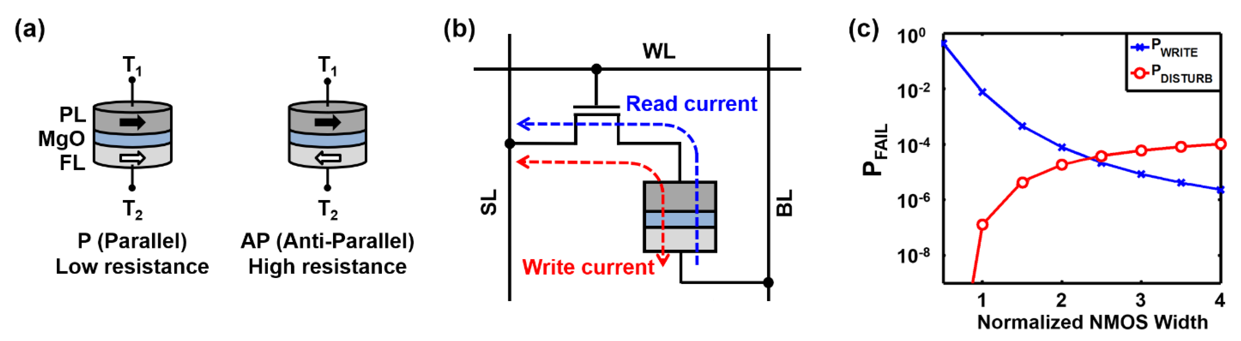
2. SOT-MRAM Fundamentals

A three-terminal SOT device is composed of MTJ and heavy metal (HM), as shown in Figure 2a. For a write operation, a charge current is passed through HM in direct contact with FL. In the bottom figure in Figure 2a, FL magnetization is initially aligned along +y direction. If a charge current is applied in −x direction, the spin-orbit coupling in HM deflects −y and +y directed spins to the top and bottom surfaces of HM, respectively. Note that the accumulated spins on the top surface exert STT, causing FL magnetization to be switched to the −y direction. The spin current injection efficiency, defined as the ratio of the injected spin current (IS) and the charge current (IC), can exceed 100%, since a single electron passing through the HM transfers multiple units of angular momentum [12,17,18]. More importantly, this switching mechanism of the SOT device enhances the reliability of MTJ, because its oxide layer is not stressed by high voltage drop [13]. For a read operation, BL is connected to a current source, SL is set to GND, and the word-line of the read access transistor is asserted high.
This biasing condition passes a small current from a terminal T1 to the terminal T3 of the SOT device, enabling the comparison of the cell voltage (VREAD) with respect to the reference voltage (VREF) using a sense amplifier.Note from Figure 2b that the read and write paths are decoupled; hence, each memory operation can be independently optimized without disturbing the other.
The SOT-MRAM cell, however, requires two access transistors, RFET for a read operation and WFET for a write operation, resulting in a larger bit-cell area compared to STT-MRAM. Consider memory cell layouts in Figure 3, where λ is half the minimum feature size. The minimum metal spacing and the minimum metal width are assumed to be 3λ [19,20] in this paper. Other design parameters are shown in Figure 3a. In general, word-lines, RWL (for a read) and WWL (for a write), run horizontally across the memory array, whereas BL and SL run orthogonally to word-lines. WRFET (WWFET) is the width of RFET (WFET). If both RFET and WFET are smaller than 9λ as in Figure 3b, i.e., if max(WRFET, WWFET) < 9λ, the horizontal dimension is limited by the metal pitch as follows.
2 W M 2 M + 2 W M = 12 λ
Otherwise, as shown in Figure 3c, the horizontal dimension is determined by the larger WRFET and WWFET as follows.
m a x ( W R F E T , W W F E T ) + W A 2 A = m a x ( W R F E T , W W F E T ) + 3 λ
The vertical dimension of SOT-MRAM is
W C + 4 W G 2 C + 2 W G + 2 W C + 2 W C 2 A + W A 2 A = 23 λ
which is due to the two-transistor requirement, twice the vertical dimension of standard STT-MRAM, shown in Figure 3d.

3. Proposed SOT-MRAM Designs
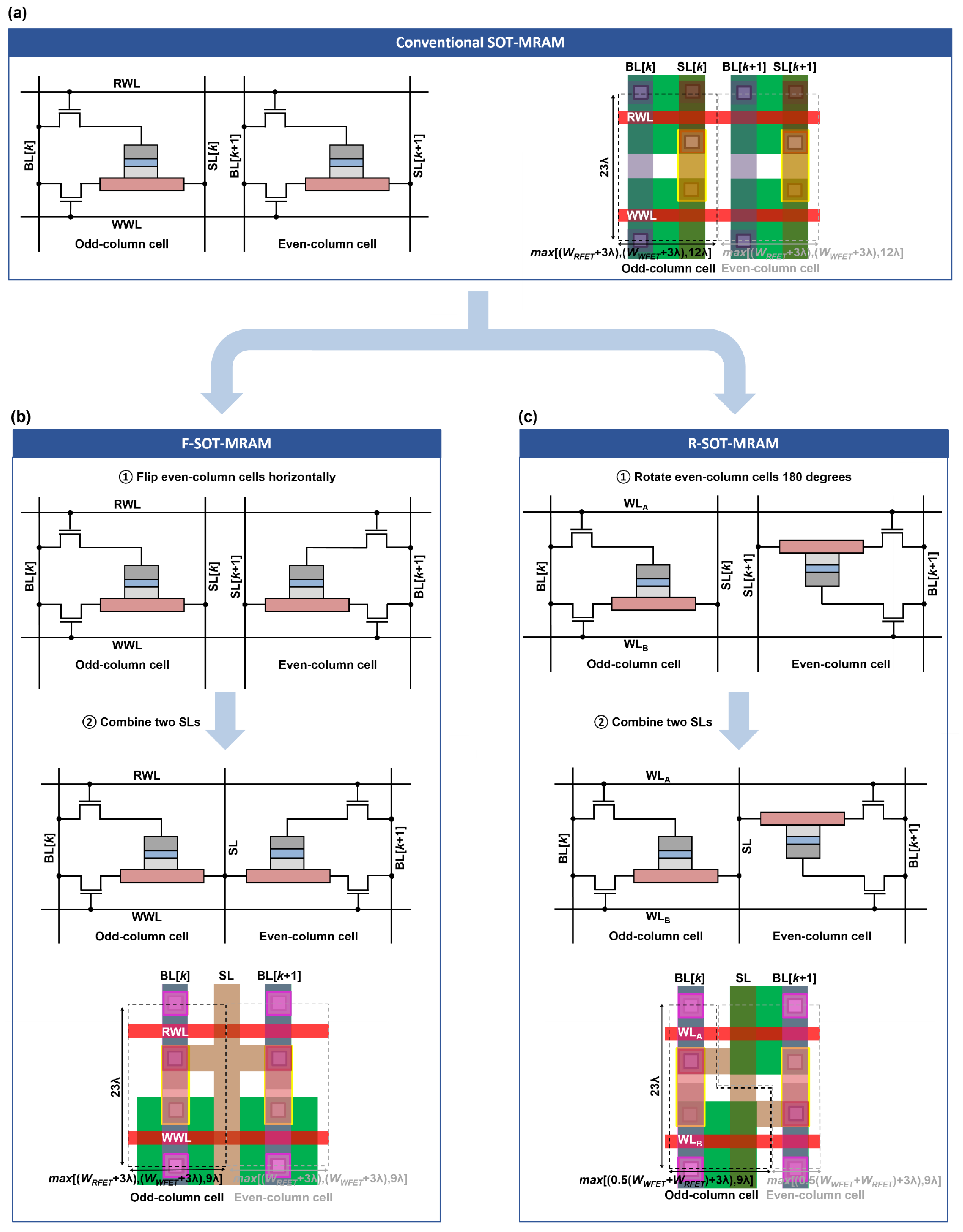
3.1. Basic Idea

In a conventional memory array containing multiple words per row, the bit-interleaving is a commonly used technique [14,15,16] (1) to reduce the risk of multi-bit errors by a radiation event and (2) to achieve a higher array density via BL multiplexing. As technology shrinks, the single radiation event due to alpha particle or neutron strikes can cause a multi-bit upset (MBU) [21]. In such case, the bit-interleaving can avoid a multi-bit error by spreading MBU over multiple different words so that each word involves at most one bit of error that can be corrected by a simple error correction code [15]. In the case of SOT-MRAM, although the magnetic storage element is immune to radiation-induced soft error, the use of bit-interleaving is still preferred, since its access transistors can suffer from MBUs [22]. In addition, the bit-interleaving is an effective means to share peripheral circuitries, thereby reducing the area of memory array [16]. Figure 4 shows an illustrative example of distance-2 bit-interleaving architecture, where two adjacent BLs, BL[k] and BL[k + 1], with k being an odd number, are multiplexed to share the sense amplifier and the write driver.
In the aforementioned bit-interleaving architecture, we observe that two adjacent bit-cells are not simultaneously accessed. This provides an opportunity for bit-cell area improvement by sharing a vertical metal line between two consecutive cells. In this work, we employed a single SL for two cells and applied the appropriate biasing conditions so that the shared SL could be used for the cell selected for access without disturbing the other cell. The following subsection describes the details of the proposed bit-cell structure, which can be applied to an array with any distance-n bit-interleaving, where n is the even number.

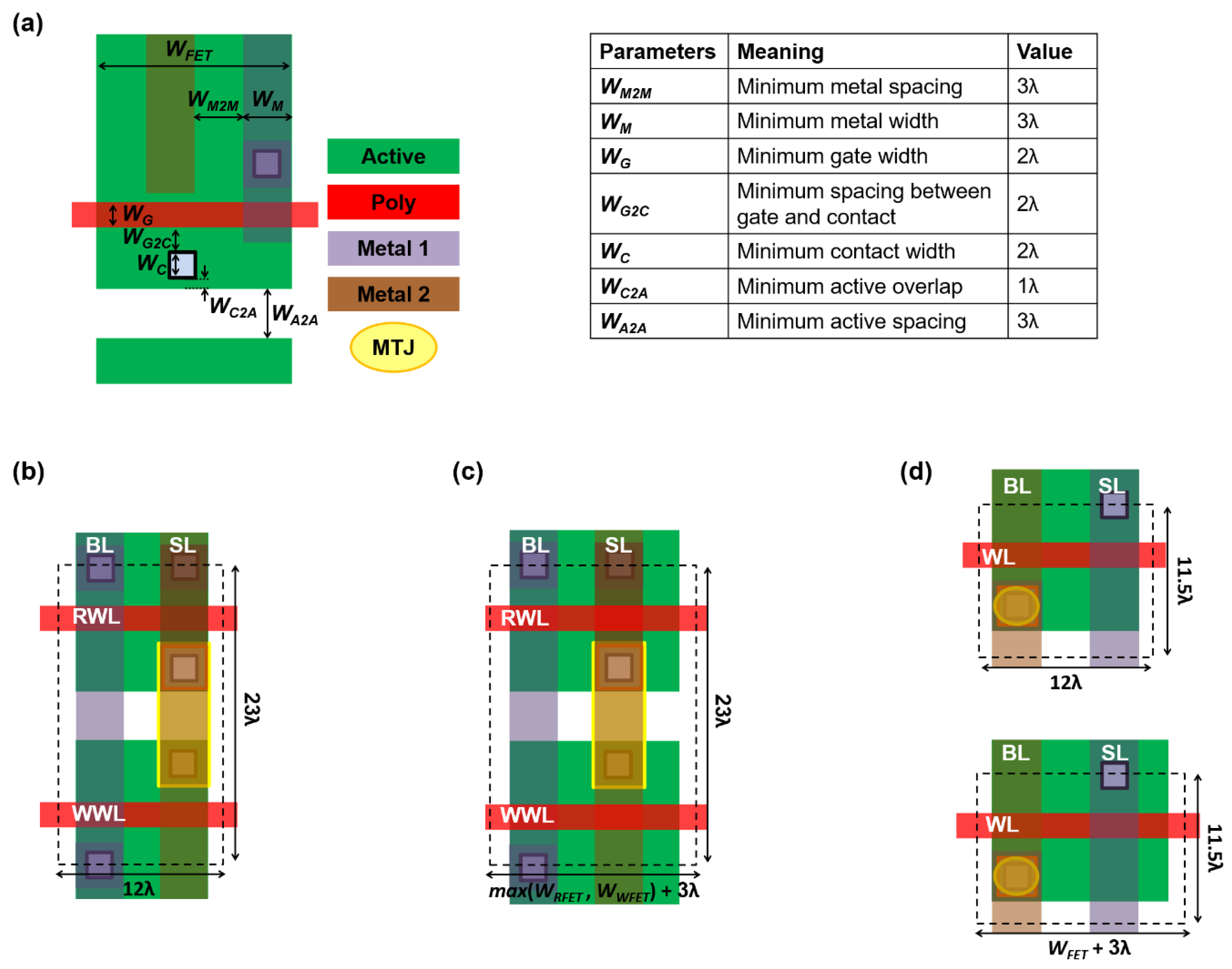
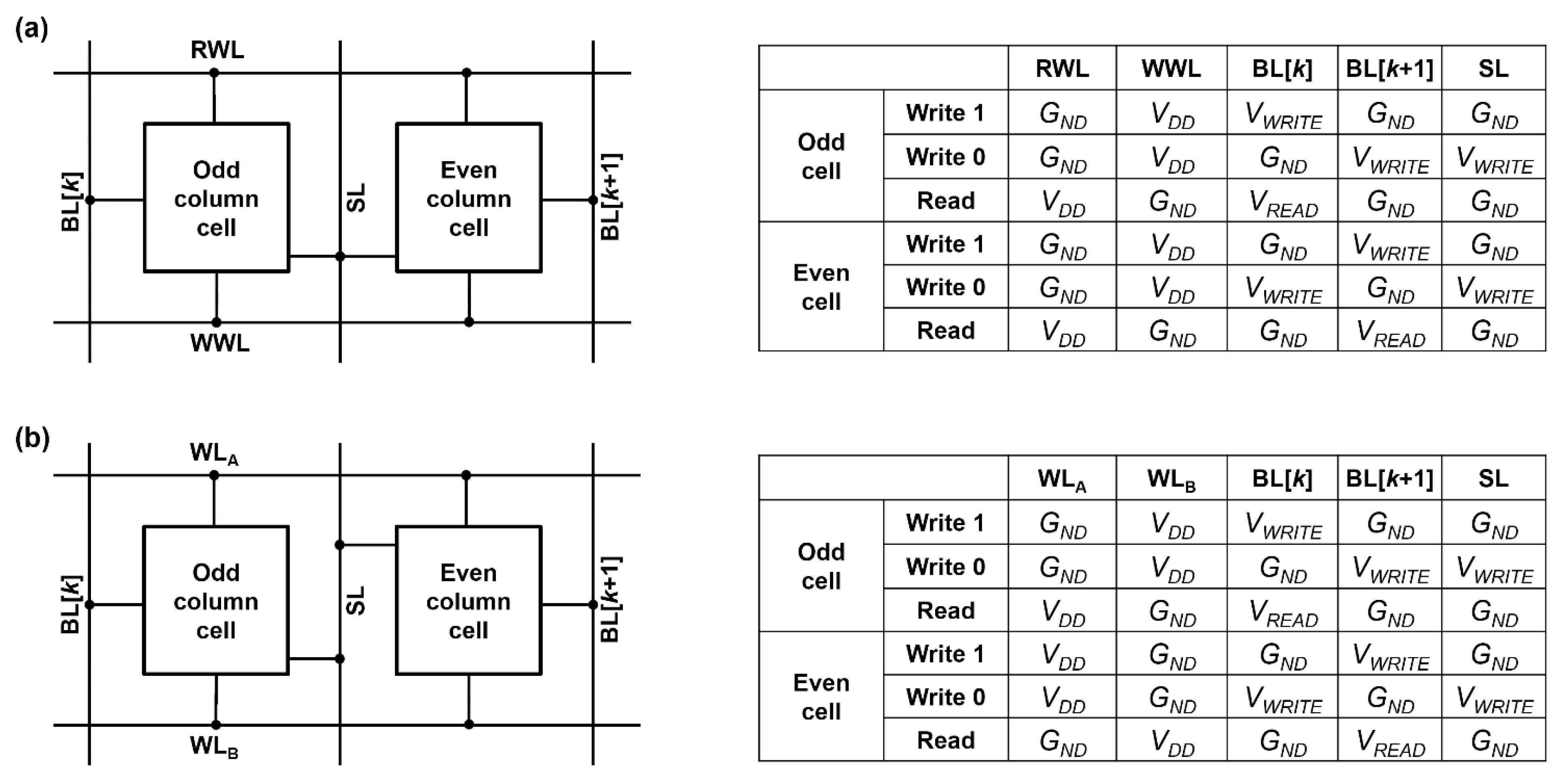
3.2. Proposed Bit-Cell Structures

We first discuss memory cell arrangements suitable for the sharing of a single SL between two adjacent cells in the same row. Consider the pair of cells in Figure 5a, where four vertical metal tracks lie in the order of BL[k], SL[k], BL[k + 1], and SL[k + 1]. In this conventional arrangement, combining two SLs into a single one can be complicated because BL[k + 1] is sandwiched between SL[k] and SL[k + 1]. To facilitate the combining of SLs, we propose to flip or rotate a cell in the even column such that SL[k + 1] precedes BL[k + 1]. The first proposed structure, termed the flipped SOT-MRAM (F-SOT-MRAM), flips an even-column cell in the horizontal direction and combines two SLs into a single one, as shown in Figure 5b. The F-SOT-MRAM can obviously improve the bit-cell area because the number of metal lines required for a pair of cells decreases from four to three. Specifically, if both RFET and WFET are sized smaller than 6λ, i.e., if max(WRFET, WWFET) < 6λ, its horizontal dimension is
1.5 W M 2 M + 1.5 W M = 9 λ
If WRFET is >6λ or WWFET is >6λ, the horizontal dimension is
m a x ( W R F E T , W W F E T ) + W A 2 A = m a x ( W R F E T , W W F E T ) + 3 λ
Shown in Figure 6a are bit-cell areas with respect to a range of max(WRFET, WWFET) for the conventional SOT-MRAM and F-SOT-MRAM. Note that the bit-cell area can be metal pitch limited (MPL) or transistor width limited (TWL) [19]. In the MPL region, F-SOT-MRAM can improve the bit-cell area by 25% compared to the conventional SOT-MRAM. If max(WRFET, WWFET) is >6λ, the bit-cell area saving diminishes as F-SOT-MRAM is in the TWL region.
The second proposed structure, namely, the rotated SOT-MRAM (R-SOT-MRAM), rotates an even-column cell by 180 degrees and combines SLs, as shown in Figure 5c. Note that the RFET of the odd-column cell and WFET of the even-column cell are connected to the same word-line, termed WLA. Similarly, the WFET of the odd-column cell and RFET of the even-column cell are connected to WLB. Under such configuration, the horizontal dimension of R-SOT-MRAM in the TWL region is determined by the mean of WRFET and WWFET, i.e.,
0.5 ( W R F E T + W W F E T ) + W A 2 A = 0.5 ( W R F E T + W W F E T ) + 3 λ
This is unlike F-SOT-MRAM, in which the horizontal dimension is independent of the smaller transistor width. Hence, R-SOT-MRAM can optimize the bit-cell area further if two access transistors are different in size. Figure 6b shows the bit-cell area of R-SOT-MRAM in comparison to F-SOT-MRAM when the absolute difference between WWFET and WRFET is λ, 2λ, and 3λ.
The biasing conditions of the proposed SOT-MRAMs are shown in Figure 7. Since a single SL is shared between two adjacent cells, a pair of cells needs an appropriate biasing so that access to one cell for memory operation does not disturb the other cell connected to the same SL. For example, to write a value of 0 into an odd-column cell in Figure 7a, BL[k] is set to GND, SL is set to VWRITE, and WWL is asserted such that the current flows from SL to BL[k]. In this case, F-SOT-MRAM applies VWRITE to BL[k + 1] to prevent the even-column cell from being unintentionally overwritten. In addition, R-SOT-MRAM needs to consider that the 180° rotation of the even-column cell alters the position of word-lines. Note from Figure 7b that WLA is used for a read operation of the odd-column cell or for a write operation of the even-column cell. Similarly, WLB is used for a write operation of the odd-column cell or for a read operation of the even-column cell.

4. Results

4.1. Simulation Framework

To evaluate our proposed memory bit-cells in comparison to conventional STT-MRAM and SOT-MRAM, we utilized a simulation framework [23] that consists of three components:
(1)
Landau–Lifshitz–Gilbert (LLG) equation solver to model the magnetization dynamics of the spintronic device [24,25,26];
(2)
Non-Equilibrium Green’s Function (NEGF) formalism to obtain the voltage-dependent resistance of MTJ [27];
(3)
SPICE simulator to model the memory bit-cell circuit.
The LLG equation solver determines the critical current for the 10 ns switching time based on the parameters in Table 1. In the case of the SOT device, the spin current injection efficiency, the ratio of IS to IC, can be calculated as [18,28]:
I S I C = A M T J A H M · θ S H ( 1 sech ( t H M λ s f ) )
where AMTJ is the cross-sectional area of the MTJ (xy-plane), AHM the cross-sectional area of the HM (yz-plane), tHM the thickness of HM, λsf a spin flip length, and θSH a spin Hall angle that is assumed to be 0.3 in our work [11]. Since AHM (=WHM × tHM) is designed to be smaller than AMTJ (=π/4 × WFL × LFL), the resultant spin current injection efficiency, 272.39%, is higher than 100%.
The resistance of HM was estimated from the experimental resistivity in [11], whereas the voltage-dependent resistance of MTJ was obtained by using the NEGF formalism [10]. The resistance function of spintronic devices was coupled with a commercial 45 nm transistor model to form the complete memory cell structure. Transient SPICE circuit simulations were performed to evaluate the energy of bit-cells at the target switching time.

4.2. Simulation Results

We evaluated four different memory bit-cells with each being designed at the same condition of 10 ns switching time; 2 ns sensing time; 15% write margin; defined as (IW-IC)/IC; and >40% read-disturb margin, defined as (IC-IR)/IC, in an array comprising 256 rows and 512 columns [29,30,31]. See Table 2 for simulation results. In the case of STT-MRAM in which the read and write current paths are identical, its access transistor needs to be sized to ensure both read and write operations. In our analysis, the transistor was sized at 430 nm, which was determined by a write operation rather than by a read operation. In the case of SOT-MRAM, the write operation at the same condition can be achieved by using the smaller transistor at 155 nm width thanks to the high spin current injection efficiency.
Nevertheless, since the conventional SOT-MRAM requires an additional transistor for a read, its bit-cell area (0.1104 µm2) is still 25% larger than that of STT-MRAM (0.0880 µm2).
In order to improve the bit-cell area, the proposed F-SOT-MRAM and R-SOT-MRAM share an SL between two adjacent bit-cells in the same row. As a result, the F-SOT-MRAM achieves a 10% reduction in bit-cell area compared to the conventional SOT-MRAM. As mentioned earlier, the R-SOT-MRAM has the potential to achieve a higher area saving if WRFET is different from WWFET. In our analysis, the R-SOT-MRAM took advantage of this potential and achieved a 25% reduction, resulting in the smallest bit-cell area among four different memory cells in Table 2.
Note that the proposed designs maintain the inherent advantages of SOT-MRAM. Due to the spin current injection efficiency of 272.39%, F-SOT-MRAM and R-SOT-MRAM achieve 45% lower write energy compared to STT-MRAM. Additionally, unlike STT-MRAM, in which the oxide thickness (tMgO) is determined by the tradeoff between read stability and write-ability, two proposed designs can optimize tMgO for a read operation only. In our work, tMgO for F-SOT-MRAM and R-SOT-MRAM was 1.30 nm, as opposed to 1.05 nm for STT-MRAM, as in Table 1. The thicker tMgO translates into the higher MTJ resistance, in turn, the smaller current required to develop the identical BL voltage during a read operation. Table 2 shows that F-SOT-MRAM and R-SOT-MRAM achieved 84% lower read energy and 2.3 × higher read-disturb margin in comparison to STT-MRAM.

5. Conclusions

We discussed area optimization techniques for high-density SOT-MRAMs. Based on the fact that adjacent columns in a bit-interleaved array are not simultaneously accessed, we proposed two design techniques to share a single source-line between two consecutive bit-cells in the same row. The proposed techniques reduce the horizontal dimension by decreasing the number of metal lines per cell while retaining the advantages of SOT-MRAM, such as high reliability and low write energy. The simulation result shows that the proposed techniques achieved a bit-cell area reduction of 10–25% without any performance overhead. Compared to STT-MRAM, our proposed designs achieved 45% lower write energy, 84% lower read energy, and 2.3 × higher read-disturb margin.

Author Contributions

Conceptualization, Y.S.; methodology, Y.S. and K.-W.K.; validation, Y.S. and K.-W.K.; formal analysis, Y.S. and K.-W.K.; investigation, Y.S. and K.-W.K.; resources, Y.S. and K.-W.K.; data curation, Y.S.; writing—original draft preparation, Y.S. and K.-W.K.; writing—review and editing, Y.S. and K.-W.K.; visualization, Y.S. and K.-W.K.; supervision, Y.S. and K.-W.K.; project administration, Y.S. and K.-W.K.; funding acquisition, Y.S. and K.-W.K. All authors have read and agreed to the published version of the manuscript.

Funding

This work was supported in part by the INHA UNIVERSITY Research Grant; the National Research Foundation of Korea (NRF) under Grant NRF-2019R1G1A1008751, Grant NRF-2020R1F1A1051529, and GrantNRF-2020M3H2A1076786, funded by the Korean government (MSIT); the Institute of Information and Communications Technology Planning and Evaluation (IITP) Grant funded by the Korean Government (MSIT) (No. 2019-0-00533, Research on CPU vulnerability detection and validation); the Next Generation Semiconductor R&D Program (No. 20009972) funded by the Ministry of Trade, Industry & Energy (MOTIE, Korea); the BK21 Four Program funded by the Ministry of Education (MOE, Korea) and National Research Foundation of Korea(NRF). The EDA Tool was supported by the IC Design Education Center.

Conflicts of Interest

The authors declare no conflict of interest.

References

  1. Chun, K.C.; Zhao, H.; Harms, J.D.; Kim, T.-H.; Wang, J.-P.; Kim, C.H. A scaling roadmap and performance evaluation of in plane and perpendicular MTJ based STT-MRAMs for high-density cache memory. IEEE J. Solid State Circuits 2013, 48, 598–610. [Google Scholar] [CrossRef]
  2. Augustine, C.; Mojumder, N.; Fong, X.; Choday, H.; Park, S.P.; Roy, K. STT-MRAMs for future universal memories: Perspective and prospective. In Proceedings of the International Conference on Microelectronics, Nis, Serbia, 13–16 May 2012; pp. 349–355. [Google Scholar] [CrossRef]
  3. Li, J.; Ndai, P.; Goel, A.; Salahuddin, S.; Roy, K. Design paradigm for robust spin-torque transfer magnetic RAM (STT MRAM) from circuit/architecture perspective. IEEE Trans. Very Large Scale Integr. (VLSI) Syst. 2009, 18, 1710–1723. [Google Scholar] [CrossRef]
  4. ITRS. 2011. Available online: http://www.itrs.net/links/2011itrs/home2011.htm (accessed on 21 August 2011).
  5. Sun, G.; Dong, X.; Xie, Y.; Li, J.; Chen, Y. A novel architecture of the 3D stacked MRAM L2 cache for CMPs. In Proceedings of the IEEE International Symposium on High Performance Computer Architecture, Raleigh, NC, USA, 14–18 February 2009; pp. 239–249. [Google Scholar] [CrossRef]
  6. Seo, Y.; Kwon, K.-W.; Fong, X.; Roy, K. High Performance and Energy-Efficient On-Chip Cache Using Dual Port (1R/1W) Spin-Orbit Torque MRAM. IEEE J. Emerg. Sel. Top. Circuits Syst. 2016, 6, 293–304. [Google Scholar] [CrossRef]
  7. Gordon-Ross, A.; Vahid, F.; Dutt, N.D. Fast Configurable-Cache Tuning With a Unified Second-Level Cache. IEEE Trans. Very Large Scale Integr. (VLSI) Syst. 2009, 17, 80–91. [Google Scholar] [CrossRef] [Green Version]
  8. Fong, X.; Kim, Y.; Choday, S.H.; Roy, K. Failure mitigation techniques for 1T-1MTJ spin-transfer torque MRAM bit-cells. IEEE Trans. Very Large Scale Integr. (VLSI) Syst. 2014, 22, 384–395. [Google Scholar] [CrossRef]
  9. Seo, Y.; Fong, X.; Roy, K. Domain wall coupling-based STT-MRAM for on-chip cache applications. IEEE Trans. Electron Devices 2015, 62, 554–560. [Google Scholar] [CrossRef]
  10. Lin., C.J.; Kang, S.H.; Wang, Y.J.; Lee, K.; Zhu, X.; Chen, W.C.; Li, X.; Hsu, W.N.; Kao, Y.C.; Liu, M.T.; et al. 45 nm low power CMOS logic compatible embedded STT MRAM utilizing a reverse-connection 1T/1MTJ cell. In Proceedings of the IEEE International Electron Devices Meeting, Baltimore, MD, USA, 7–9 December 2009; pp. 11.6.1–11.6.4. [Google Scholar] [CrossRef]
  11. Pai, C.-F.; Liu, L.; Li, Y.; Tseng, H.W.; Ralph, D.C.; Buhrman, R.A. Spin transfer torque devices utilizing the giant spin Hall effect of tungsten. Appl. Phys. Lett. 2012, 101, 122404. [Google Scholar] [CrossRef]
  12. Liu, L.; Pai, C.-F.; Li, Y.; Tseng, H.W.; Ralph, D.C.; Buhrman, R.A. Spin-torque switching with the giant spin Hall effect of tantalum. Science 2012, 336, 555–558. [Google Scholar] [CrossRef] [PubMed] [Green Version]
  13. Seo, Y.; Kwon, K.-W.; Roy, K. Area-Efficient SOT-MRAM with a Schottky Diode. IEEE Electron Device Lett. 2016, 37, 982–985. [Google Scholar] [CrossRef]
  14. Nayak, D.; Acharya, D.P.; Nanda, U. A high stable 8T-SRAM with bit interleaving capability for minimization of soft error rate. Microelectron. J. 2018, 73, 43–51. [Google Scholar] [CrossRef]
  15. Shi, Y.Q.; Zhang, X.M.; Ni, Z.-C.; Ansari, N. Interleaving for combating bursts of errors. IEEE Circuits Syst. Mag. 2004, 4, 29–42. [Google Scholar] [CrossRef]
  16. Baeg, S.; Wen, S.; Wong, R. SRAM Interleaving Distance Selection with a Soft Error Failure Model. IEEE Trans. Nucl. Sci. 2009, 56, 2111–2118. [Google Scholar] [CrossRef]
  17. Hoffmann, A. Spin Hall effects in metals. IEEE Trans. Magn. 2013, 49, 5172–5193. [Google Scholar] [CrossRef]
  18. Kim, Y.; Fong, X.; Kwon, K.-W.; Chen, M.-C.; Roy, K. Multilevel spin-orbit torque MRAMs. IEEE Trans. Electron Devices 2015, 62, 561–568. [Google Scholar] [CrossRef]
  19. Gupta, S.K.; Park, S.P.; Mojumder, N.N.; Roy, K. Layout-aware optimization of STT-MRAMs. In Proceedings of the Design, Automation & Test in Europe Conference & Exhibition, Dresden, Germany, 12–16 March 2012; pp. 1455–1458. [Google Scholar] [CrossRef]
  20. Liebman, L. DfM, the teenage years. In Proceedings of the SPIE Advanced Lithography, San Jose, CA, USA, 24–29 February 2008; Volume 6925, p. 692502. [Google Scholar] [CrossRef]
  21. Maiz, J.; Hareland, S.; Zhang, K.; Armstrong, P. Characterization of multi-bit soft error events in advanced SRAMs. In Proceedings of the IEEE International Electron Devices Meeting, Washington, DC, USA, 8–10 December 2003; pp. 21.4.1–21.4.4. [Google Scholar] [CrossRef]
  22. Yang, Y.; Wang, P.; Zhang, Y.; Cheng, Y.; Zhao, W.; Chen, Y.; Li, H.H. Radiation-Induced Soft Error Analysis of STT-MRAM: A Device to Circuit Approach. IEEE Trans. Comput. Aided Des. Integr. Circuits Syst. 2016, 35, 380–393. [Google Scholar] [CrossRef]
  23. Fong, X.; Gupta, S.K.; Mojumder, N.N.; Choday, S.H.; Augustine, C.; Roy, K. KNACK: A Hybrid Spin-Charge Mixed-Mode Simulator for Evaluating Different Genres of Spin Transfer Torque MRAM Bit-cells. In Proceedings of the International Conference on Simulation of Semiconductor Processes and Devices, Osaka, Japan, 8–10 September 2011; pp. 51–54. [Google Scholar] [CrossRef]
  24. Slonczewski, J.C. Current-driven excitation of magnetic multilayers. J. Magn. Magn. Mater. 1996, 159, L1–L7. [Google Scholar] [CrossRef]
  25. Sankey, J.C.; Cui, Y.-T.; Sun, J.Z.; Slonczewski, J.C.; Buhrman, R.A.; Ralph, D.C. Measurement of the spin-transfer-torque vector in magnetic tunnel junctions. Nat. Phys. 2007, 4, 67–71. [Google Scholar] [CrossRef] [Green Version]
  26. Gilbert, T.L. A phenomenological theory of damping in ferromagnetic materials. IEEE Trans. Magn. 2004, 40, 3443–3449. [Google Scholar] [CrossRef]
  27. Datta, D.; Behin-Aein, B.; Salahuddin, S.; Datta, S. Quantitative Model for TMR and Spin-Transfer Torque in MTJ Devices. In Proceedings of the International Electron Devices Meeting, San Francisco, CA, USA, 6–8 December 2010; pp. 22.8.1–22.8.4. [Google Scholar] [CrossRef]
  28. Manipatruni, S.; Nikonov, D.E.; Young, I.A. Voltage and energy-delay performance of giant spin hall effect switching for magnetic memory and logic. arXiv 2013, arXiv:1301.5374. [Google Scholar]
  29. Li, H.; Jagannathan, B.; Wang, J.; Su, T.-C.; Sweeney, S.; Pekarik, J.J.; Shi, Y.; Greenberg, D.; Jin, Z.; Groves, R.; et al. Technology Scaling and Device Design for 350 GHz RF Performance in a 45 nm Bulk CMOS Process. In Proceedings of the IEEE Symposium on VLSI Technology, Kyoto, Japan, 12–14 June 2007; pp. 56–57. [Google Scholar] [CrossRef]
  30. Guan, Z.; Marek-Sadowska, M.; Nassif, S. Statistical analysis of process variation induced SRAM electromigration degradation. In Proceedings of the International Symposium on Quality Electronic Design, Santa Clara, CA, USA, 3–5 March 2014; pp. 700–707. [Google Scholar] [CrossRef]
  31. Dong, Q.; Wang, Z.; Lim, J.; Zhang, Y.; Sinangil, M.E.; Shih, Y.-C.; Chih, Y.-D.; Chang, J.; Blaauw, D.; Sylvester, D. A 1-Mb 28-nm 1T1MTJ STT-MRAM with Single-Cap Offset-Cancelled Sense Amplifier and In Situ Self-Write-Termination. IEEE J. Solid State Circuits 2019, 54, 231–239. [Google Scholar] [CrossRef]
Figure 1. (a) Magnetic tunnel junction (MTJ) device structure; (b) read and write current paths of spin-transfer torque magnetic random-access memory (STT-MRAM); (c) probability of write failure and probability of disturb failure with respect to a range of access transistor width [8].
Electronics 10 00792 g001
Figure 2. (a) Spin-orbit torque (SOT) device structure; (b) high-density spin-orbit torque magnetic random-access memory (SOT-MRAM) bit-cell; (c) biasing condition for write and read.
Electronics 10 00792 g002
Figure 3. (a) Parameters for layout design rules; (b) conventional SOT-MRAM when max(WRFET, WWFET) is smaller than 9λ; (c) conventional SOT-MRAM when max(WRFET, WWFET) is greater than 9λ; (d) conventional STT-MRAM when its access transistor WFET is smaller than 9λ [top] or greater than 9λ [bottom].
Electronics 10 00792 g003
Figure 4. Illustrative example of distance-2 bit-interleaving architecture.
Electronics 10 00792 g004
Figure 5. Schematic and layout of (a) conventional SOT-MRAM, (b) F-SOT-MRAM, and (c) R-SOT-MRAM.
Electronics 10 00792 g005
Figure 6. (a) Bit-cell area comparison between conventional SOT-MRAM and F-SOT-MRAM; (b) bit-cell area comparison between F-SOT-MRAM and R-SOT-MRAM. Bit-cell area is metal pitch limited (MPL) or transistor width limited (TWL).
Electronics 10 00792 g006
Figure 7. Biasing conditions of (a) F-SOT-MRAM and (b) R-SOT-MRAM.
Electronics 10 00792 g007
Table 1. Parameters of storage devices.
Device ParametersSTT DeviceSOT Device
Gilbert damping, α0.0070.0122
Saturation magnetization, MS1100 × 103 A/m1100 × 103 A/m
Dimension of FL (WFL × LFL × tFL)120 nm × 40 nm × 2.5 nm 1120 nm × 40 nm × 2.5 nm 2
Dimension of HM (WHM × LHM × tHM)-120 nm × 80 nm × 2.7 nm
HM resistivity-200 µΩ·cm
Spin Hall angle, θSH-0.3
Spin flip length, λsf-1.40 nm
MgO thickness, tMgO1.05 nm1.30 nm
Critical current for 10 ns switching time206 µA121 µA
1,2 MTJ free layer has an elliptical shape.
Table 2. Comparison of different bit-cells.
STT-MRAMConventional
SOT-MRAM
F-SOT-MRAMR-SOT-MRAM
Transistor width (nm)430155 (WWFET)
85 (WRFET)
155 (WWFET)
85 (WRFET)
155 (WWFET)
85 (WRFET)
Bit-cell area (µm2)0.08800.11040.09890.0828
Write energy per bit (fJ)2737.31504.01508.41508.4
Read energy per bit (fJ)267.442.342.342.3
Read-disturb margin (%)41939393
Publisher’s Note: MDPI stays neutral with regard to jurisdictional claims in published maps and institutional affiliations.

