Article

A 2.1 GHz, 210 μW, —189 dBc/Hz DCO with Ultra Low Power DCC Scheme

1
Institute of Microelectronics of the Chinese Academy of Sciences, Beijing 100029, China
2
Institue of Microelectronics, University of Chinese Academy of Sciences, Beijing 100049, China
*
Authors to whom correspondence should be addressed.
Electronics 2021, 10(7), 805; https://doi.org/10.3390/electronics10070805
Submission received: 8 February 2021 / Revised: 26 March 2021 / Accepted: 26 March 2021 / Published: 29 March 2021
(This article belongs to the Section Circuit and Signal Processing)

Abstract

:
This article presents a low power digital controlled oscillator (DCO) with an ultra low power duty cycle correction (DCC) scheme. The DCO with the complementary cross-coupled topology uses the controllable tail resistor to improve the tail current efficiency. A robust duty cycle correction (DCC) scheme is introduced to replace self-biased inverters to save power further. The proposed DCO is implemented in a Semiconductor Manufacturing International Corporation (SMIC) 40 nm CMOS process. The measured phase noise at room temperature is −115 dBc/Hz at 1 MHz offset with a dissipation of 210 μ W at an oscillating frequency of 2.12 GHz, and the resulin figure-of-merit is s −189 dBc/Hz.
Keywords:
DCO; DCC; ultra low power

1. Introduction

The power consumption and the phase noise of a digital controlled oscillator (DCO) determine the digtal phase locked loops (DPLL) performance. The trend towards low power design of DPLL [1,2,3,4,5] is driven by the requirements of the low power and low cost communication systems, therefore the low power design of DCOs appeared.
Several approaches to save power consumption of integrated oscillators have attracted favors from both industry and academia. On the whole, there are two main methods to reduce power consmuption—improvement of current effeciency and improvement of voltage effciency. The Class-C LC oscillator [6,7,8,9,10] is the typical topology for improving current effeciency. Compared with traditional Class-B oscillators, Class-C topologies exploit currents in operating trasistors and enlarge the first harmonic of the currents. However, the Class-C toplogies need start-up circuts to start the ocsillating and put the differential pair into Class-C operation [11,12,13,14] which increase the difficulty of designing and extra power consumption. Moreover, the LC ocsillator with a LC tail filter [15,16] is the structure for imporing voltage current. The harmonic frequency of the LC tail filter is twice the frequency of oscillating and the output amplitude can be enhanced without extra current. In other words, if the voltage amplitude is fixed, then the current consumption is saved. Nevertheless, this structure suffers drawbacks of low frequency range and extra area of inductors. Another toplogy with transformers [2] can also improve the voltage effeciency. But this circuit suffers the difficulty of transformers.
In addition to the above structures, a topology that saves power without a complex structure is introduced, as in Figure 1. The complementary cross-coupled topology reuses the bias current and limits the output amplitude. The bias current is provided by a tail resistor [17]. Compared to Class-C oscillators, current efficiency can be improved by increasing the resistance of R, and no start-up problem occurs.
It is worth mentioning that, as R increases, the peak level of V P and V N decrease and the duty cycle problem of the output signal is serious. For the double data rate (DDR) systems and half/quarter-rate serial link transceivers, the duty cycle of the clock signals must be 50% accurately. Hence, a duty cycle correction (DCC) is necessary for the DCO. From previous studies [18,19,20,21,22], wide frequency range and high precision designs are introduced. Nevertheless, their structures are complicated and the power consumptions are high. A simple approach can be carried out by self-biased inverters (as in Figure 1). However, the power consumption of the self-biased inverters are significant, as well, and the coupling capacitors provide heavy loads to the DCO.
Based on the problem mentioned above, this letter proposes an ultra low power DCC scheme for a low power complementary cross-coupled DCO.

2. DCO with Ultra Low Power DCC Scheme

2.1. Conceptual Architecture

The main objective of this study is to design a duty cycle correction scheme for a low power DCO to replace the self-biased inverter and to obtain lower power consumption in the overall design. Since the tail resistor in Figure 1 is changeable, a possible solution to compensate the output duty cycle deviation of the DCO is to add another changeable bottom tail resistor in which resistance can be adaptively adjusted to a suitable value according to the duty cycle. Therefore, it is necessary to create a negative feedback loop. Figure 2 shows the conceptual diagram of the proposed DCC scheme. The duty cycle of the output signals V O U T P and V O U T N are monitored by a duty cycle detector in which output signal V D is compared with a reference voltage V R E F . V D is then sent to be connected to a voltage-controlled tail resistor to ensure that the duty cycle is maintained at 50%.
As R changes, if the duty cycle is higher than 50%, the DCC loop would decrease the resistance of R V C ; if the duty cycle is lower than 50%, the loop would increase the resistance of R V C . Enough closed loop gain would ensure a high accuracy of duty cycle correction against process, voltage, and temperature (PVT) variation.

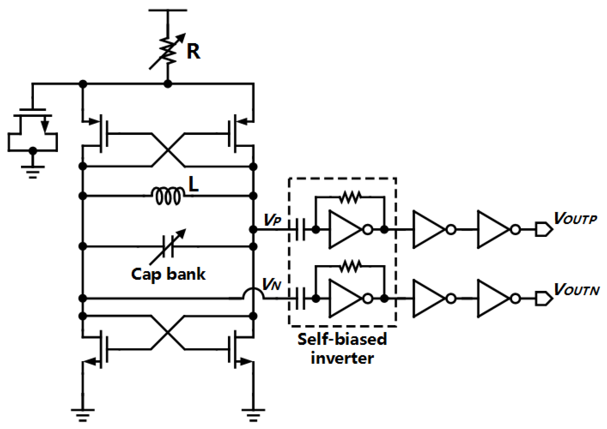
2.2. Circuit Implementation

The goal is to design a DCC scheme with an ultra low power and high accuracy. Therefore, the negative feedback should use simple circuit structure (low power purpose) and provide high enought loop gain (high accuracy purpose).
Figure 3 presents the circuit implementation of the proposed DCO with an ultra low power DCC scheme. Compared with Figure 2, the DCC loop includes three main stages: a duty cycle detector, a comparator, and a voltage controlled resistor.
The duty cycle detector consists just two resistors R 1 and R 2 . Since signals V O U T P and V O U T N have the same DC component and totally opposite AC components, the duty cycle detector R 1 and R 2 can extract DC level at V B without any filter because the AC components are canceled at V B . To avoid signals V O U T P and V O U T N disturbing each other, the resistance of R 1 and R 2 should large enough (say 100 k Ω ).
The comparator is implemented by an operational amplifier (OA). The structure is shown, as in Figure 4. The gain of the OA is relaxed. However, the power consumption is significant in the DCC loop. Therefore, it is not necessary to use a complex topology to boost the gain and the current flows can be saved in the simple structure (just including two current flows). Moreover, small aspect ratios of transistors would save power further and 1 μ m/6 μ m and 2 μ m/6 μ m of W/L are chosen for NMOS and PMOS, respectively.
The voltage controlled resistor can be easily employed by a NMOS tail transistor M 1 . The R O N of M 1 is controlled by the output signal V B of the OA. Since M 1 reuses the current flowing in the tail resistor R, there is no extra power consumption from M 1 .
The accuracy of the V R E F must be guaranteed for a high accurate DCC scheme. Since the goal of a DCC scheme is 50% duty cycle, V R E F should be V D D / 2 . Therefore, a low-power, high-accurate voltage divider is required. A resistive divider may be a suitable choice, but it requires a large area to provide enough resistance to save power. Hence, we use two identical PMOS transistors with small aspect ratios to implement the voltage divider as shown in Figure 3. Since the substrate nodes of the PMOS transistors can be connected to the source nodes and the electrical environment of each PMOS M 2 and M 3 is the same, this structure can produce an accurate V D D / 2 .
Finally, we add two MOS capacitors M 4 and M 5 to filter the noise from R (thermal noise) and M 1 (flicker noise and thermal noise).

2.3. DCC Loop Analysis

As mentioned above, the DCC scheme is a negative feedback loop. To ensure a high accurate calibration of duty cycle, the loop gain should be large enough. Thus, the stability of the multi-pole system must be adjusted carefully.
To reduce the complexity of analysis, we simplify the DCC loop, as in Figure 5. Since the AC components of oscillating signals have no influence on the DCC loop, the LC tank can be ignored. Two inverter chains are simplified as one chain to provide DC component. Furthermore, the tail resistor R and two pairs of cross coupled transistors are treated as equivalent resistors R e q 1 and R e q 2 .
The equivalent circuit clearly shows that there are three contributors to the loop gain: the inverter chain, OA and the common source amplifier (consisting of M 1 , R e q 1 and R e q 2 ). Since the inverter chain can provide a large enough DC gain, the OA gain in the loop is not as significant as mentioned above, which is the reason why a complex structure is not needed to boost the OA gain. Although the large DC gain is generated by the inverter chain, the output impedance of the inverter is small due to the small gate length. In addition, the parasitic capacitances at V 3 and V D are small and can be neglected. Therefore, the poles from the inverter are far from the origin and have negligible effect on the stability of the loop.
Because of large load capacitor (noise filtering capacitor M 5 ) at V 1 and large output impedance of the OA at V B , the DCC loop can be treated as a second order system. To ensure the stability of the loop, we carry out the Miller compensation by adding a miller capacitor C C and nulling resistor R Z connecting between V B and V 1 .
To analyze this system, the closed loop can be broken at V D , as in Figure 6.
The open loop transfer function (from V R E F to V D 2 ) is:
G ( s ) = V D 2 V R E F = A i n v × R e q 1 R e q 1 + R e q 2 × g m r o ( R e q 1 + R e q 2 ) ( g m 1 ( R Z + ( s C C ) 1 ) 1 ) C M 5 C C r o ( R e q 1 + R e q 2 ) s 2 + g m 1 C C r 0 ( R e q 1 + R e q 2 ) s + 1
where A i n v is the DC gain of the inverter chain, g m is the transconductance of the input transistors of the OA, r o is the output impedance of the OA, g m 1 is the transconductance of the tail transistor M 1 , and C M 5 is the capacitance of the noise filtering capacitor M 5 .
Then, the closed loop transfer function is as follows:
H ( s ) = G ( s ) G ( s ) 1 .
The dominant pole p 1 , the highest nondominant pole p 2 and the zero in the open loop can be easily obtained as Equations (3)–(5).
p 1 = 1 r o ( R e q 1 + R e q 2 ) g m 1 C C ,
p 2 = g m 1 C M 5 ,
z = 1 R Z C C / g m 1 .
According to Equations (3) and (4), the distance of p 1 and p 2 are moved away from each other by Miller effect and that improves the stability of the loop.
In order to eliminate the influence of zero, the zero can be moved to infinity by adjusting the nulling resistor as Equation (6).
R Z = C C g m 1 .
To verify the stability of the DCC loop, a post-layout transient simulation is carried out, as in Figure 7.
Figure 7 shows that the DCO starts to oscillate ( V O U T P in Figure 7) at about 0.6 μ s after powering up. Then, the DCC circuit starts to calibrate the duty cycle of the output signals and the calibration finished at about 2.75 μ s. According to the shapes of signal V B and V D , it indicates that the DCC loop is a underdamping system which verifies the stability of the loop.

3. DCC Accuracy, Power Consumption and Phase Noise

3.1. DCC Accuracy

In order to verify the high accuracy and the robustness of the DCC scheme among the process variation, transient simulations with different process corners are carried out, as in Figure 8. The results indicates that the accuracy is 50 ± 0.6%.
To display the function of the DCC scheme visually, the comparsion between the DCO without and with the DCC scheme is presented, as in Figure 9.

3.2. Power Consumption and Phase Noise

As analyzed in [23,24,25], the tail current have both influence on the power consumption and the phase noise of a DCO. A trade-off between these two parameters always appears which means lower power results in larger phase noise. Hence, to find a specific value of tail current which has the highest efficiency, the relation of power and phase noise should be considered carefully. According to [26], a normalized figure of merit (FoM) is introduced to demonstrate the trad-off:
F o M = L ( f o f f s e t ) 20 l o g f 0 f o f f s e t + 10 l o g P D C O 1 m W ,
where L ( f o f f s e t ) is the phase noise of the oscillation carrier, f o f f s e t is the offset frequency from the oscillation carrier, f 0 is the center frequency of the oscillation carrier, and P D C O is the power consumption of the DCO. The lower value of FoM means the higher efficiency of current consumption. The tail resistor in Figure 1 and Figure 3 are designated to be changeable for the search of the lowest FoM.
Although the proposed topology has the lower power DCC scheme, the extra circuit (such as the OA and voltage divider) would contribute extra phase noise through the tail transistor M 1 . The simulations are performed to reveal the phase noise (at 1 MHz offset) in the tail current for the purpose of observing this phenomenon as shown in Figure 10.
It is worth mentioning that the results in Figure 10 of conventional circuit (in Figure 1) are not from results in [17] because values of inductance, capacitances, and transistor sizes are not the same with the proposed application. Therefore, to make a fair comparison, we re-design the conventional circuit. Since this re-design has not been fabricated, the comparison between the conventional and the proposed circuits is based on simulation results.
Figure 10 can be broken into two regions. If the tail current is large enough (Region II), the DCC circuit would have seriously negative influence on the phase noise performance of the proposed DCO. However, two lines are closed with each other which illustrates that if the tail current is small enough (Region I), the extra noise is not a significant trouble for low power design. FoMs against the tail current in two topologies presents in Figure 11. It is seen that the proposed circuit has lower FoM. We can conclude that the proposed DCC scheme saves much power by costing little performance of noise.
Table 1 and Table 2 list the power dissipation for the two designs at a tail current of 152 μ A, respectively. The DCC scheme only consumes 4.3% of the total power of the circuit, while the self-biased inverter consumes 34%. It is worth mentioning that the inverter used for self-biased inverter is a standard cell with W/L of transistor sizes of 1.22 μ m/40 nm for PMOS and 520 nm/40 nm for NMOS, respectively.

4. Measurement Results

The proposed DCO is fabricated in 40 nm CMOS technology and the chip micrograph is shown, as in Figure 12. The area of the chip is 590 × 320 μ m 2 . The chip measurement setup is shown, as in Figure 13. A Rohde & Schwarz FSW50 signal and spectrum analyzer was used to test the phase noise of the DCO, as shown in Figure 14. When the proposed circuit is oscillating at 2.12 GHz, the measured phase noise is −115 dBc/Hz at a 1 MHz offset. In addition, the measured power dissipation is 210 μ W, and the calculated FoM value is −189 dBc/Hz, which is close to the simulation results in Section 3.2.
Table 3 shows the results of this study compared with the results of previous LC oscillators. The DCO achieves good current efficiency while achieving ultra-low power dissipation.
Some discussions should be mentioned as following. Although, the VCO in [13] needs additional blocks to provide bias voltages for Class-C structure, the extra digital control circuits powers down when the calibration is done, so the extra power consumption can be ignored. Moreover, the design in [14] also needs an operational amplifier to finish Class-C operation, however, the extra power dissipation is just 0.18 mW which can also be neglected. Therefore, the additional blocks’ power in [13,14] do not have much influence on the calculation of FoM in Table 3.

5. Conclusions

This paper proposes a low-power DCO with an ultra-low-power DCC scheme. The DCO based on complementary cross-coupled topology with a controllable tail resistor to improve the efficiency of tail current. A robust DCC scheme is introduced to replace the self-biased inverter for further power savings. After careful design, the presented DCO is highly suitable for low power digital phase-locked loops.

Author Contributions

Conceptualization, S.Z.; formal analysis, S.Z. and J.Z.; investigation, S.Z.; resources, S.Z.; data curation, S.Z.; writing—original draft preparation, S.Z.; writing—review and editing, S.Z., J.Z., and Y.Z.; visualization, S.Z.; supervision, J.Z. and Y.Z.; project administration, Y.Z.; funding acquisition, Y.Z. All authors have read and agreed to the published version of the manuscript.

Funding

This research received no external funding.

Conflicts of Interest

The authors declare no conflict of interest.

References

  1. Un, K.-F.; Qi, G.; Yin, J.; Yang, S.; Yu, S.; Ieong, C.-I.; Mak, P.-I.; Martins, R.P. A 0.12-mm2 1.2-to-2.4-mW 1.3-to-2.65-GHz Fractional-N Bang-Bang Digital PLL With 8-μs Settling Time for Multi-ISM-Band ULP Radios. IEEE Trans. Circuits Syst. Regul. Pap. 2019, 9, 3307–3316. [Google Scholar] [CrossRef]
  2. Liu, H.; Sun, Z.; Huang, H.; Deng, W.; Siriburanon, T.; Pang, J.; Wang, Y.; Wu, R.; Someya, T.; Shirane, A.; et al. A 265-μW Fractional-N Digital PLL With Seamless Automatic Switching Sub-Sampling/Sampling Feedback Path and Duty-Cycled Frequency-Locked Loop in 65-nm CMOS. IEEE J. Solid-State Circuits 2019, 12, 3478–3492. [Google Scholar] [CrossRef]
  3. Seong, T.; Lee, Y.; Yoo, S.; Choi, J. A 320-fs RMS Jitter and −75-dBc Reference-Spur Ring-DCO-Based Digital PLL Using an Optimal-Threshold TDC. IEEE J. Solid-State Circuits 2019, 9, 2501–2512. [Google Scholar] [CrossRef]
  4. Kuo, F.-W.; Babaie, M.; Chen, H.-N.R.; Cho, L.-C.; Jou, C.-P.; Chen, M.; Staszewski, R.B. An All-Digital PLL for Cellular Mobile Phones in 28-nm CMOS with −55 dBc Fractional and −91 dBc Reference Spurs. IEEE Trans. Circuits Syst. Regul. Pap. 2018, 11, 3756–3768. [Google Scholar] [CrossRef]
  5. Tsai, C.-H.; Zong, Z.; Pepe, F.; Mangraviti, G.; Craninckx, J.; Wambacq, P. Analysis of a 28-nm CMOS Fast-Lock Bang-Bang Digital PLL With 220-fs RMS Jitter for Millimeter-Wave Communication. IEEE J. Solid-State Circuits 2020, 7, 1854–1863. [Google Scholar] [CrossRef]
  6. Mazzanti, A.; Andreani, P. Class-C Harmonic CMOS VCOs, With a General Result on Phase Noise. IEEE J. Solid-State Circuits 2008, 12, 2716–2729. [Google Scholar] [CrossRef]
  7. Fanori, L.; Andreani, P. Highly Efficient Class-C CMOS VCOs, Including a Comparison With Class-B VCOs. IEEE J. Solid-State Circuits 2013, 7, 1730–1740. [Google Scholar] [CrossRef]
  8. Mazzanti, A.; Andreani, P. A Push–Pull Class-C CMOS VCO. IEEE J. Solid-State Circuits 2013, 3, 724–732. [Google Scholar] [CrossRef]
  9. Shirazi, A.H.M.; Nikpaik, A.; Molavi, R.; Lightbody, S.; Djahanshahi, H.; Taghivand, M.; Mirabbasi, S.; Shekhar, S. On the Design of mm-Wave Self-Mixing-VCO Architecture for High Tuning-Range and Low Phase Noise. IEEE J. Solid-State Circuits 2016, 5, 1210–1222. [Google Scholar] [CrossRef]
  10. Lim, C.C.; Ramiah, H.; Yin, J.; Kumar, N.; Mak, P.-I.; Martins, R.P. A 5.1-to-7.3 mW, 2.4-to-5 GHz Class-C Mode-Switching Single-Ended-Complementary VCO Achieving >190 dBc/Hz FoM. IEEE Trans. Circuits Syst. Express Briefs 2019, 7, 237–241. [Google Scholar] [CrossRef]
  11. Deng, W.; Okada, K.; Matsuzawa, A. Class-C VCO With Amplitude Feedback Loop for Robust Start-Up and Enhanced Oscillation Swing. IEEE J. Solid-State Circuits 2013, 2, 429–440. [Google Scholar] [CrossRef]
  12. Perticaroli, S.; Toso, S.D.; Palma, F. A Harmonic Class-C CMOS VCO-Based on Low Frequency Feedback Loop: Theoretical Analysis and Experimental Results. IEEE Trans. Circuits Syst. Regul. Pap. 2014, 9, 2537–2549. [Google Scholar] [CrossRef]
  13. Li, C.; Liscidini, A. Class-C PA-VCO Cell for FSK and GFSK Transmitters. IEEE Trans. Circuits Syst. Regul. Pap. 2016, 7, 1537–1546. [Google Scholar] [CrossRef]
  14. Liao, X.; Liu, L. A Low-Voltage Robust Class-C VCO With Dual Digital Feedback Loops. IEEE Trans. Circuits Syst. Express Briefs 2020, 11, 2347–2351. [Google Scholar] [CrossRef]
  15. Hegazi, E.; Sjöland, H.; Abidi, A.A. A Filtering Technique to Lower LC Oscillator Phase Noise. IEEE J. Solid-State Circuits 2001, 12, 1921–1930. [Google Scholar] [CrossRef] [Green Version]
  16. Murphy, D.; Darabi, H.; Wu, H. Implicit Common-Mode Resonance in LC Oscillators. IEEE J. Solid-State Circuits 2017, 3, 812–821. [Google Scholar] [CrossRef]
  17. Chillara, V.K.; Liu, Y.-H.; Wang, B.; Ba, A.; Vidojkovic, M.; Philips, K.; Groot, H.d.; Staszewski, R.B. An 860 μW 2.1-to-2.7GHz all-digital PLL-based frequency modulator with a DTC-assisted snapshot TDC for WPAN (Bluetooth Smart and ZigBee) applications. In Proceedings of the 2014 IEEE International Solid-State Circuits Conference Digest of Technical Papers (ISSCC), San Francisco, CA, USA, 9–13 February 2014. [Google Scholar]
  18. Mu, F.; Svensson, C. Pulsewidth control loop in high-speed CMOS clock buffers. IEEE J. Solid-State Circuits 2000, 2, 134–141. [Google Scholar]
  19. Qiu, Y.; Zeng, Y.; Zhang, F. 1–5 GHz duty-cycle corrector circuit with wide correction range and high precision. Electron. Lett 2014, 11, 792–794. [Google Scholar] [CrossRef]
  20. Cheng, K.-H.; Su, C.-W.; Chang, K.-F. A High Linearity, Fast-Locking Pulsewidth Control Loop With Digitally Programmable Duty Cycle Correction for Wide Range Operation. IEEE J. Solid-State Circuits 2008, 2, 399–413. [Google Scholar] [CrossRef]
  21. Ha, J.C.; Lim, J.H.; Kim, Y.J.; Jung, W.Y.; Wee, J.K. Unified all-digital duty-cycle and phase correction circuit for QDR I/O interface. Electron. Lett 2008, 22, 1300–1301. [Google Scholar] [CrossRef]
  22. Zhang, Z.; Zhu, G.; Yue, C.P. A 2-to-10 GHz 1.4-mW 50% Duty-Cycle Corrector in 40-nm CMOS Process. In Proceedings of the International Conference on Electron Devices and Solid State Circuits, Shenzhen, China, 6–8 June 2018. [Google Scholar]
  23. Berny, A.D.; Niknejad, A.M.; Meyer, R.G. A 1.8-GHz LC VCO With 1.3-GHz Tuning Range and Digital Amplitude Calibration. IEEE J. Solid-State Circuits 2005, 4, 909–917. [Google Scholar] [CrossRef]
  24. Soltanian, B.; Kinget, P.R. Tail Current-Shaping to Improve Phase Noise in LC Voltage-Controlled Oscillators. IEEE J. Solid-State Circuits 2006, 4, 1792–1802. [Google Scholar] [CrossRef]
  25. Andreani, P.; Kozmin, K.; Sandrup, P.; Nilsson, M.; Mattsson, T. A TX VCO for WCDMA/EDGE in 90 nm RF CMOS. IEEE J. Solid-State Circuits 2011, 7, 1618–1626. [Google Scholar] [CrossRef]
  26. Kinget, P. Integrated GHz Voltage Controlled Oscillators. In Analog Circuit Design; Sansen, W., Huijsing, J., Van De Plassche, R., Eds.; Kluwer Academic Publishers: Boston, MA, USA, 1999; pp. 1–29. [Google Scholar]
Figure 1. Low power digital controlled oscillator (DCO) with a tail resistor.
Electronics 10 00805 g001
Figure 2. Conceptual architecture of proposed DCO with duty cycle correction (DCC) scheme.
Electronics 10 00805 g002
Figure 3. Proposed low power DCO with an ultra low power DCC scheme.
Electronics 10 00805 g003
Figure 4. Structure of low power operational amplifier.
Electronics 10 00805 g004
Figure 5. Equivalent circuit of proposed DCC loop.
Electronics 10 00805 g005
Figure 6. Open loop circuit of proposed DCC loop.
Electronics 10 00805 g006
Figure 7. Transient simulation results for verifying stability.
Electronics 10 00805 g007
Figure 8. DCC accuracy among different process corners.
Electronics 10 00805 g008
Figure 9. Transient simulation results for duty cycle: (a) without DCC scheme; (b) with DCC scheme.
Electronics 10 00805 g009
Figure 10. Comparison of the phase noise against tail current.
Electronics 10 00805 g010
Figure 11. Comparison of figure of merit (FoM) against tail current.
Electronics 10 00805 g011
Figure 12. Chip micro-photo.
Electronics 10 00805 g012
Figure 13. Measurement setup.
Electronics 10 00805 g013
Figure 14. Measurement result of phase noise.
Electronics 10 00805 g014
Table 1. Power break-down of the proposed DCO.
DCODCC SchemeTotal
Power ( μ W)2019210
Table 2. Power break-down of the traditional DCO.
DCOSelf-Biased InvertersTotal
Power ( μ W)204103307
Table 3. Performance comparison.
Tech.Freq.Tuning RangePhase NoisePowerFoM
(nm)(GHz)(%)(dBc/Hz)(mW)(dBc/Hz)
This work402.1232−115 @ 1 MHz0.21−189
[10]1302.470.6−130 @ 1 MHz7.3−189
[13]1302.4513.2−132 @ 2.5 MHz2.5−188
[14]1802.5520.4−123 @ 1 MHz1.28−190
[24]2502.1219.0−118 @ 0.6 MHz2.25−185
[25]902.5546.2−156 @ 20 MHz22.8−188
Publisher’s Note: MDPI stays neutral with regard to jurisdictional claims in published maps and institutional affiliations.

