Abstract
Wireless devices such as smart meters, trackers, and sensors need connections at multiple frequency bands with low power consumption, thus requiring multiband and efficient antenna systems. At the same time, antennas should be small to easily fit in the scarce space existing in wireless devices. Small, multiband, and efficient operation is addressed here with non-resonant antenna elements, featuring volumes less than 90 mm3 for operating at 698–960 MHz as well as some bands in a higher frequency range of 1710–2690 MHz. These antenna elements are called antenna boosters, since they excite currents on the ground plane of the wireless device and do not rely on shaping complex geometric shapes to obtain multiband behavior, but rather the design of a multiband matching network. This design approach results in a simpler, easier, and faster method than creating a new antenna for every device. Since multiband operation is achieved through a matching network, frequency bands can be configured and optimized with a reconfigurable matching network. Two kinds of reconfigurable multiband architectures with antenna boosters are presented. The first one includes a digitally tunable capacitor, and the second one includes radiofrequency switches. The results show that antenna boosters with reconfigurable architectures feature multiband behavior with very small sizes, compared with other prior-art techniques.
1. Introduction
With the advent of the everything-connected era, antennas play a very significant role. From smart meters and smart trackers to sensors and any other Internet of Things (IoT) device, every wireless device needs at least one antenna to transmit and receive information. In response, the wireless industry is moving fast to launch new devices into this growing market. This fact pushes RF or microwave and wireless engineers to design radiofrequency chains in a smart way, using off-the-shelf devices such as filters, amplifiers, diplexers, and front-end modules. At the end of this radiofrequency chain, an antenna is needed to efficiently transmit and receive electromagnetic waves. Accordingly, an off-the-shelf antenna component would be an attractive selection for simplifying the entire design process. It would not only simplify the antenna design phase, but also the device manufacturing process, reducing costs and being compatible with pick-and-place machines for mass production.
Besides off-the-shelf antenna components, a miniature size and multiband performance are two other demanding requirements for wireless antenna systems. Common techniques to design small and multiband antennas for wireless devices rely on complex geometries, where the several resonant modes of the antenna determine the frequency bands of operation [1,2,3,4,5,6,7,8,9,10,11]. On the one hand, this procedure requires a high level of expertise to shape the antenna geometry correctly and achieve acceptable behavior to operate at the frequency bands of interest. This complexity of the antenna geometry shaping process makes RF or microwave and wireless engineers reluctant to design their own antennas for wireless systems. On the other hand, some currently available off-the-shelf antennas are mainly narrowband, while others, although multiband, are difficult to adjust to the bands of interest once they are integrated inside the device. The off-the-shelf antenna proposed here overcomes these shortcomings. A very small and simple element can be integrated inside any wireless device for operating at any frequency band through the proper adjustment of a matching network. The antenna element can be easily adjusted not by modifying its geometry, but through the proper matching network design. This is a simpler, faster, and more familiar method for RF or microwave and wireless engineers who are acquainted with matching networks at every single stage of a telecommunication system (e.g., filters and amplifiers). Therefore, designing a multiband antenna system with this technique is more related to a microwave circuit design than to an antenna geometry design, thus making antenna design much more like filter design than conventional antenna design.
The antenna technology relies on a non-resonant antenna element that is electrically short in terms of the operating wavelength (~λ/30). Its correct location on a ground plane of a wireless device enables the excitation of efficient radiating modes on the ground plane [12,13,14,15,16,17]. Therefore, the term antenna booster is adopted here to refer to this non-resonant antenna element. Antenna boosters are miniature, surface-mount, off-the-shelf components that replace conventional customized PIFA and printed antennas for mobile or wireless connectivity applications (Figure 1). However, since the antenna booster is electrically small, its impedance is mainly reactive, and thus it is poorly matched at most of the bands of operation in the frequency range from 0.6 GHz up to 10.6 GHz, where many communication systems are allocated, such as cellular and short-range wireless communications. This mismatch issue is overcome with the addition of a multiband matching network, resulting in a multiband antenna system with a small antenna element and with competitive efficiency values [12,13,14,15,16,17].
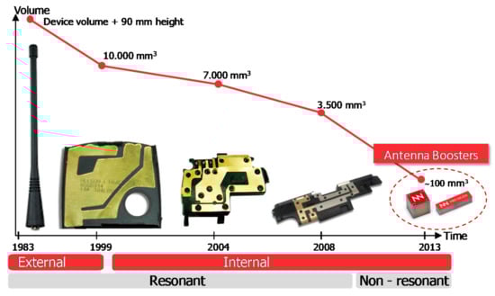
Figure 1.
Progression from external, quarter wavelength monopole antennas to internal custom antennas based on complex geometries to the tiny, off-the-shelf antenna boosters.
Examples of antennas combined with matching networks are found in the literature [18,19,20,21,22,23,24,25,26,27,28,29,30]. However, all those designs rely on adding intelligence to the antenna geometry. In addition, in all the above cases, the antenna still represents a considerable volume. Although the volumes of the antennas have been continuously shrunk, they still rely on complex geometries (Figure 1). On the contrary, antenna boosters can still operate at multiple frequency bands while keeping a very small antenna volume [12,13,14,15,16,17].
In this paper, multiband operation is addressed with antenna boosters combined with reconfigurable matching networks, comprising lumped passive components (capacitors and inductors) as well as active devices. In a first case, a digitally tunable capacitor is shown, and in a second case, a switch-based solution is adopted. This results in reconfigurable matching networks, useful for tuning the frequency bands of operation. It is important to emphasize that a passive matching network can provide multiband operation. However, adding reconfigurability adds a new degree of freedom to expand the number of bands beyond the ones that can be achieved with a passive matching network. Moreover, as a second advantage, reconfigurability can advantageously be applied to retune the frequency bands of operation in wireless devices when exposed to different, harsh surroundings such as conductive bodies, concrete, wood, and plastics, which shift the frequency response of the antenna. Finally, the multiband behavior for small form factor devices (<50 mm × 50 mm) is challenged. Therefore, a reconfigurable antenna-booster architecture is convenient, because an antenna booster is small enough to be embedded into a small device, and reconfigurability provides connections at multiple frequency bands.
The paper is structured as follows. An introduction to antenna booster technology is explained in Section 2. Multiband reconfigurable matching networks using digitally tunable capacitors (DTCs) and RF switches are described in Section 3 and Section 4, respectively. A comparison with prior-art multiband reconfigurable antennas is discussed in Section 5. Finally, conclusions are drawn in Section 6.
2. Antenna Booster Technology
Antenna booster-based technology relies on very small antenna elements called antenna boosters to provide operation in a wireless device (Figure 1 and Figure 2)—[13]. The same antenna booster as the one depicted in Figure 2 can operate at different bands, depending on the matching network. This is a different approach than conventional antenna designs, where the antenna geometry must be created case by case, thus increasing the time and cost. In addition, the same antenna booster can operate for different platform sizes, since only the matching network changes from one platform to another [31]. This is a faster and easier approach to designing multiband antenna systems than designing an antenna from scratch.
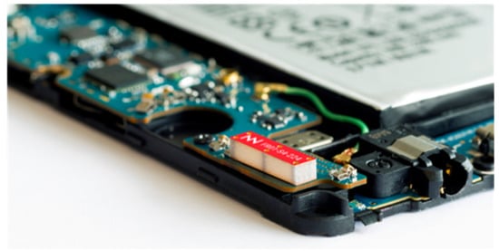
Figure 2.
An antenna booster (in red) located on a PCB (Printed Circuit Board) of a wireless device. Its tiny size (12 mm × 3 mm × 2.4 mm (height)) allows easy integration of the antenna booster within the device.
To illustrate the non-resonant nature of an antenna booster, an antenna booster (a 3D, brass-made parallelepiped in this example) of 12 mm × 3 mm × 2.4 mm (height) was analyzed, which represented a maximum size of only λ/35.8 at 698 MHz. The antenna booster was integrated in a ground plane featuring dimensions of 120 mm × 60 mm (Figure 3a). Said antenna booster was in charge of exciting radiating modes in the ground plane, which became the relevant part of the radiation process. This fact justifies the antenna booster name, since it boosted currents on the ground plane (Figure 4) [13]. From a practical perspective, the corners of the ground plane provided the best bandwidth and efficiency [17].
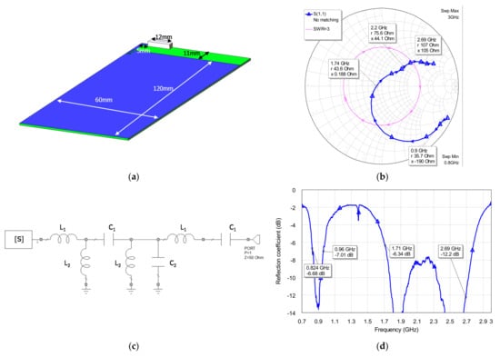
Figure 3.
(a) Antenna booster on a 120 mm × 60 mm ground plane over a dielectric substrate (εr = 4.15, tanδ = 0.013, and h = 1 mm). The antenna booster is a 12 mm × 3 mm × 2.4 mm (height) 3D conductive parallelepiped. (b) Simulated input impedance, showing a reactive capacitive behavior at the low frequency region (698–960 MHz). (c) A passive matching network for achieving multiband behavior (L1 = 4.3 nH, L2 = 18 nH, C3 = 0.9 pF, C4 = 1 pF, L5 = 13 nH, C6 = 2 pF, and L7 = 4.5 nH). (d) Reflection coefficient resulting from adding the matching network of (c) to the antenna system shown in (a).
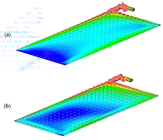
Figure 4.
Simulated current distribution for the antenna booster shown in Figure 3a at (a) 850 MHz and (b) 2200 MHz. Most of the current is aligned with the long edge at 850 MHz, whereas the current at 2200 MHz has both directions: one aligned with the long edge and the other with the short edge. This current distribution depends on the ground plane size as well as the position of the antenna booster. Blue color represents the lowest intensity and red de maximum.
The input impedance was reactive, most particularly at the low bands (698–960 MHz), where the impedance was mainly capacitive (Figure 3b). A passive matching network could match the antenna system shown in (Figure 3c), covering 824–960 MHz up to 1710–2690 MHz, as shown in [17,32]. However, the frequency range from 698 MHz to 824 MHz would not be properly matched (Figure 3d). This frequency range is needed in many wireless devices, such as smart trackers. This frequency range represents 16% of the bandwidth, which supposes a significant challenge since it is located at the lower frequencies of operation. Therefore, in those situations where a passive matching network cannot squeeze more bandwidth, reconfigurability is a good option. In this sense, and with the aim of improving the performance in the frequency range of 698–960 MHz up to 1710–2200 MHz or 2690 MHz, reconfigurable matching architectures in combination with antenna boosters are proposed using digitally tunable capacitors (DTCs) and radio frequency switches in Section 3 and Section 4, respectively.
3. Digitally Tunable Capacitors for Antenna Boosters
The bandwidth of an antenna system cannot be infinitely enlarged by adding more components to a matching network, owing to the Fano limit [33]. To avoid such a drawback and increase the bandwidth to allocate more frequency bands, a tunable capacitor is strategically included in the passive matching network, resulting in a reconfigurable circuit. Hence, the reconfigurable circuit comprises lumped capacitors and inductors and a digitally tunable capacitor [34].
This section presents a multiband antenna system comprising an antenna booster and a reconfigurable matching network to cover 698–960 MHz and 1710–2690 MHz.
3.1. Digitally Tunable Capacitors
A digitally tunable capacitor (DTC) is a microwave device where the capacitance can be digitally changed within a range from Cmin to Cmax. The tuning ratio (Cmax/Cmin) is intrinsically related to the DTC quality factor (Q); the larger the tuning ratio, the lower the Q value is [35]. The microelectromechanical system (MEMS) technology DTC from Cavendish Kinetics (now Qorvo) for this design presented a value of Q = 700 at Cmax = 1 pF at 700 MHz with a tuning ratio of 2.5. Thanks to the low intrinsic losses of MEMS technology, the DTC featured a high Q with a small footprint. In the present case, the DTC area was only 1.4 mm × 1.4 mm (Figure 5).
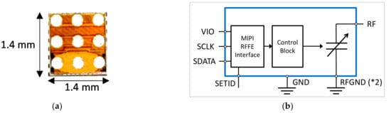
Figure 5.
(a) Footprint of the digitally tunable capacitor (DTC). (b) Block diagram of the DTC, where the capacitor can be tuned from 0.4 pF to 1.0 pF. The equivalent series resistance (ESR) was ~0.3 Ω at Cmax with a 5-bit resolution (32 capacitor states). The self-resonant frequency (SRF) was >15 GHz. The RF power handling was +39 dBm, and there was high linearity. For the Mobile Industry Processor Interface (MIPI) radio frequency front-end (RFFE) interface, the small size was ~2 mm2, and the low power was a typical 180 µW.
Besides 1.8 V (VIO, Figure 5), RF ground, and RF input connections, it supported the Mobile Industry Processor Interface (MIPI) radio frequency front-end (RFFE) interface with one clock (SCLK, Figure 5) and one series data (SDATA, Figure 5). With a 5-bit resolution in the digital control, there were 32 programmable capacitor states from 0.4 pF to 1.0 pF with a constant step size of 18 fF. The MIPI RFFE was compatible with other radiofrequency components and baseband processors in the system, which could select the state of the DTC based on the desired use condition. In the prototype described here, the state was selected using an MIPI master interface controlled by a laptop application. Once the state was set, the MIPI digital cable bus was disconnected in order to not interfere with the impedance and radiation measurements. An on-board battery and voltage regulator provided power to the DTC.
3.2. A Reconfigurable Matching Network with a DTC
A small antenna booster (86.4 mm3) was proposed for multiband operation in combination with a reconfigurable matching network [36]. The antenna booster was placed at the corner of a ground plane, featuring the dimensions (120 mm × 60 mm) of a wireless IoT device (Figure 6). Said reconfigurable matching network used the DTC implemented with MEMS described in the previous section. The RFFE digital signals for capacitance selection were provided through a removable ribbon cable. For the present case, only four states were enough to cover the frequency range of 698–960 MHz up to 1710–2690 MHz.
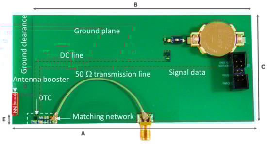
Figure 6.
The antenna booster with the reconfigurable matching network and its control circuit. The control lines from the battery and RFFE interface to the tunable capacitor go underneath the ground plane (B × C) shown in the top layer of the board. A = 131 mm, B = 120 mm, C = 60 mm, E = 5 mm, and D = 8 mm.
Analysis was done using electromagnetic simulation of the PCB, including the antenna booster. The S-parameters computed with the electromagnetic simulation were then imported in a circuit simulator (cadence AWR Microwave Office) to design the matching network, comprising a combination of lumped capacitors, inductors, and the tunable capacitor. Once the simulation showed feasible results, a reference board was built (Figure 6).
The proposed reconfigurable matching network comprising a shunt DTC is shown in Figure 7. The programmable states for the DTC were S00 (0.40 pF), S02 (0.44 pF), S08 (0.55 pF), and S27 (0.92 pF).
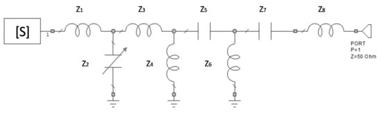
Figure 7.
Reconfigurable matching network where Z2 is the DTC. Z1 = 8 nH, Z3 = 7.3 nH, Z4 = 11 nH, Z5 = 0.8 pF, Z6 = 13 nH, Z7 = 1.9 pF, and Z8 = 2.5 nH. All passive components were SMD (Surface-Mount Device) 0402 type, with a high Q and tight tolerance (from Murata).
The state of the DTC was software-controlled with a parallel interface connection at the end of the ground plane. Since the ground plane was a relevant element for the radiation process, to avoid an undesired effect of the interface connection, the following set-up was prepared. The DTC was DC-powered with a small battery embedded on the ground plane (Figure 6). Then, a particular state of the DTC was selected, having the interface connection attached. Once the DTC was operating at a given state, the interface connection was removed. Since the DTC received DC voltage from the battery, the state was maintained, and thus both S11 and total efficiency measurements could be carried out without the impact of the interface connection. The typical power consumption of the DTC was 180 μW, which represented about 2% of the power of a transceiver.
After optimizing the matching network, some relevant states were chosen to cover the range of 698–960 MHz up to 1710–2690 MHz (Figure 8).
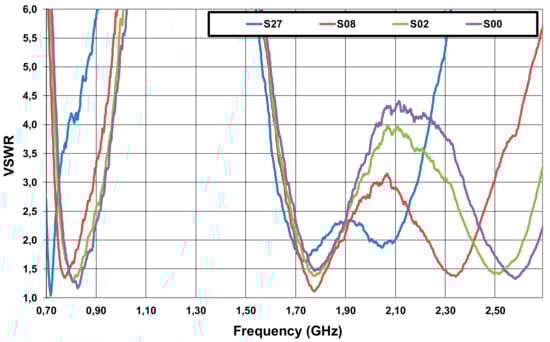
Figure 8.
Measured VSWR for four states: S27, S08, S02, and S00.
It was shown from the VSWR measurements that a particular state (S27) could cover some low bands of 700 MHz, namely those from 698 MHz to 746 MHz. From 746 MHz up to 824 MHz, the S08 state could be selected. It is remarkable that four states were almost enough to obtain an acceptable VSWR for the whole frequency range (Figure 8).
To analyze the radiation performance, the total efficiency (ηt) was measured inside an anechoic chamber using 3D pattern integration (Satimo Stargate-32). The total efficiency considered both the radiation efficiency (ηr) and the mismatch losses as follows: ηt = ηr × (1−|S11|2) (Figure 9). The gain results were also measured using the same set-up, resulting in an average gain of 1.5 dBi and 1.1 dBi at the low-frequency region and the high-frequency region, respectively. Radiation patterns are like those of a half-wavelength dipole, which are suitable for wireless environments since the wireless device may receive radio signals from any direction.
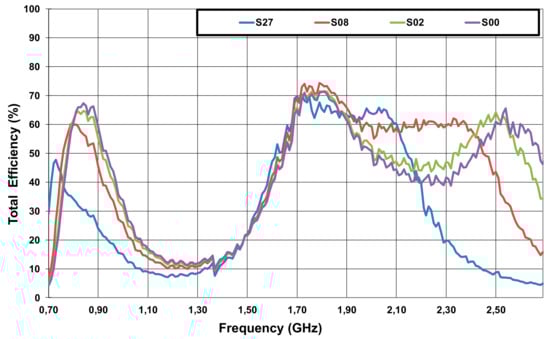
Figure 9.
Measured total efficiency for the same four states shown in Figure 8.
In order to summarize the results, the average total efficiency values for several representative communication systems, namely LTE-12 (699–746 MHz), LTE-13, LTE-14 (746–798 MHz), LTE-5 (824–894 MHz), LTE-8 (880–960 MHz), LTE-3 (1710–1880 MHz), LTE-2 (1850–1990 MHz), LTE-1 (1920–2170 MHz), LTE-30 (2305–2360 MHz), and LTE-41 (2496–2690 MHz), are gathered in Table 1. The information in Table 1 helped to choose the best state for a specific LTE band, shown in a dark color. For example, regarding the low frequency region, if operation were needed at LTE-12, the S27 state should be selected, providing an average efficiency value of 41.5%. If LTE-13–14 were desired, then state S08 should be selected. For LTE-5 and 8, S00 could be selected. The same criteria applied for the high-frequency region. For example, to cover LTE-3, state S08 could be selected. S08 could be chosen for covering LTE-2, 1 and 30. Finally, S00 could be selected for covering LTE-41.

Table 1.
Measured total efficiencies for four states. The shadow indicates the best state for each frequency region.
Due to the limitations of the anechoic chamber below 700 MHz, only measurements up to state S27 were carried out. However, tuning could go below 700 MHz, since more states were available.
To sum up, a small antenna booster of 86.4 mm3 and a reconfigurable matching network allowed coverage in the frequency bands from 698 MHz to 960 MHz and from 1710 MHz to 2690 MHz. To achieve competitive performance, the reconfigurable matching network was designed using a MEMS tunable capacitor (DTC) combined with lumped inductors and capacitors. The measured average total efficiency was above 40% and 57% at the 698–960 MHz and 1710–2690 MHz frequency ranges, respectively, making the architecture attractive for multiband wireless devices.
4. RF Switches for Antenna Boosters
The DTC-based matching network for antenna boosters shown in the previous section is very attractive when only one component (a capacitor) of the matching network can tune the frequency bands of operation. However, in other situations, changing only the value of a capacitor is not enough to achieve satisfactory performance at the frequency bands of interest. This is the case of the following example illustrating a small platform (50 mm × 50 mm) to operate at several cellular frequency bands from 698 MHz to 960 MHz and from 1710 MHz to 2200 MHz, as well as at 1575 MHz for geolocalization (Figure 10).
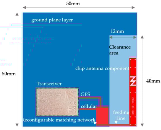
Figure 10.
An antenna booster component (in red) on a PCB (50 mm × 50 mm) connected to a reconfigurable matching network with single-pole n-throw (SPNT) switches connected to a transceiver for cellular and GPS communication.
In the present case, to gain more freedom, the multiband operation was addressed with simple matching networks comprising one or two lumped components designed for matching a particular frequency band. In this regard, a set of matching networks were connected using two single-pole N-throw (SPNT) switches as shown in the coming sections.
4.1. SPNT Switch
SPNT switches permit connecting a common radiofrequency input (pole) to several output ports (throws) (Figure 11). Besides the number of throws, insertion loss and isolation form an important figure of merit, since it impacts both the transmitted and received signal strength [37]. For the present case, the insertion loss of the SP8T switch is 0.5 dB and 0.7 dB at 698 MHz and 2170 MHz, respectively, with a power handling of 32 dBm. Isolation is typically better than 40 dB at the whole frequency range of operation.
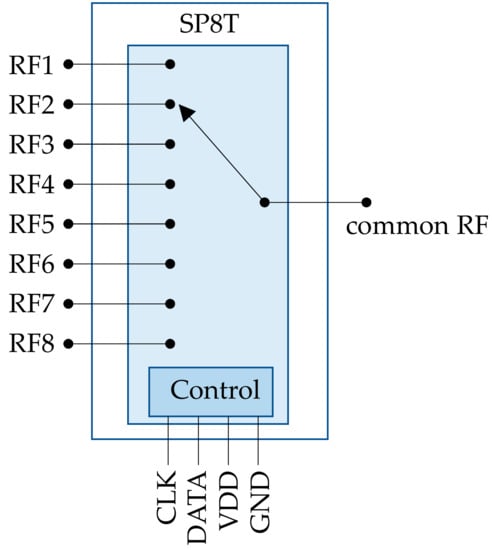
Figure 11.
An SP8T switch includes a common RF port, eight throws, and a control interface to set a connection between an RFi and the common RF.
For an SPNT switch, N can adopt values from 2 up to 12, where each state can be controlled either with a general-purpose input/output (GPIO) or an RFFE interface. The GPIO interface comprises control lines to set the state of the switch, based on a simple DC voltage-driven scheme. For example, for an SP8T, three control lines are needed to control eight states: RF1 using 001, RF2 using 010, and so on. RFFE simplifies the number of control lines (1 clock and 1 data) and employs a single-ended CMOS input/output port, minimizing power consumption [38].
In the following section, a pair of SP8T switches having 2 mm × 2 mm size are included to provide operation at both cellular and GPS bands using an antenna booster of only 90 mm3.
4.2. Multiband Operation with an SP8T Switch
A multiband reconfigurable architecture comprising an antenna booster with a bunch of matching networks is proposed for operation at cellular bands, as well as GPS (Figure 12) [39]. A first simulation analysis was carried out, simulating a PCB as shown in Figure 10, including an antenna booster of 30 mm × 3 mm × 1 mm (h). Once the S-parameters at the antenna port were obtained, the matching network architecture, including the passive matching networks and the RF switches, was designed. Once the design was feasible from the simulation domain, the solution was implemented into a real cellular IoT device (Figure 13).
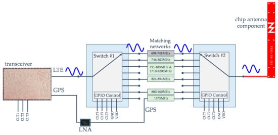
Figure 12.
Reconfigurable matching network system for multiband operation. A transceiver (cellular and GPS) controls the SP8T switches through lines CLT1–3, matching networks comprising lumped SMD components (capacitors and inductors). A low noise amplifier (LNA) amplifies the GPS signal before entering the transceiver.
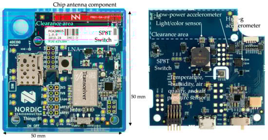
Figure 13.
A 50 mm × 50 mm IoT open platform device (Thingy:91 by Nordic Semiconductor), including the reconfigurable antenna system of Figure 12. Besides cellular and GPS operation thanks to the reconfigurable antenna system (by Ignion), many sensors for IoT applications are included, such as temperature, humidity, air quality, air pressure, color, and light data [39].
The cellular frequency band of operation was automatically controlled by a transceiver (by Nordic Semiconductor) through a GPIO interface, although an RFFE interface could be used as well. Such a GPIO interface controls the SP8T switches with three control lines (CLT1–3). In this case, six matching networks were designed with circuit simulator software (Cadence AWR Microwave Office) including the measured S-parameters of the switches as well as the S-parameters of the SMD components of the matching network. Those matching networks were used to match different cellular bands as well as GPS. For each frequency band, a simple L-type matching network using SMD components was used (Figure 14).
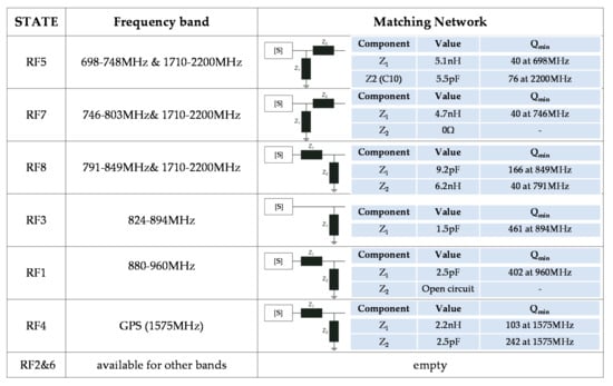
Figure 14.
Matching networks for cellular and GPS, used in the electric scheme shown in Figure 12 where the box with [S] includes the S11 of switch #2 and the antenna booster.
To keep the solution as compact as possible at the cellular bands, SMD 0201 (0.5 mm × 0.25 mm) lumped capacitors and inductors were used for the matching networks, selecting the highest quality factor (Q) possible. For the 1575 MHz matching network, SMD 0402-lumped components were used to achieve a higher Q (Figure 14).
Each matching network provided operation at a single band (RF1, RF3, or RF4) or dual band (RF5, RF7, or RF8) with an S11 value that was optimized within the band (Figure 15).
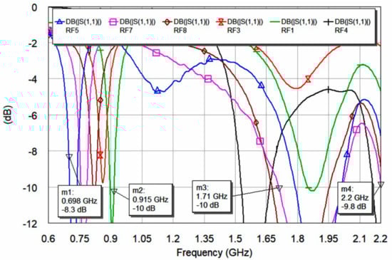
Figure 15.
S11 for several states covering cellular and GPS bands. Each state corresponds to one matching network as shown in Figure 14.
For each state, the total efficiency was measured in an anechoic chamber using 3D pattern integration. As stated before, total efficiency considered mismatching as well as losses of the system, such as those of the antenna system, and the nearby components (e.g., the lithium polymer battery under the PCB) as well as the top and bottom plastic covers (Table 2).
Table 2.
Measured total efficiency for the IoT device shown in Figure 13, including all components and top and bottom plastic casings.
5. Discussion
This section discusses several reconfigurable antenna solutions that have appeared in industry, as well as the scientific literature [40,41,42,43,44,45,46,47,48,49,50,51,52,53,54]. The selection criteria included those reconfigurable antenna solutions for multiband behavior at two frequency regions: a first one from 698 MHz to 960 MHz and a second one from 1.71 GHz to at least 2.17 GHz. The first frequency region was by far the most challenging for designers, since the antennas were electrically smaller in this first frequency region than in the second. Consequently, it was more difficult to squeeze bandwidth from the first frequency region.
The antennas were classified by length and width. In those antennas having irregular shapes, the length and width were selected as the minimum rectangle comprising the antenna. Once all antennas were put in a single map, a length and width average could be calculated. That single average antenna defined four quadrants: the best, the worst, and two intermediate quadrants, one having a length below the average but widths above and the other way around for the other intermediate quadrant (Figure 16).
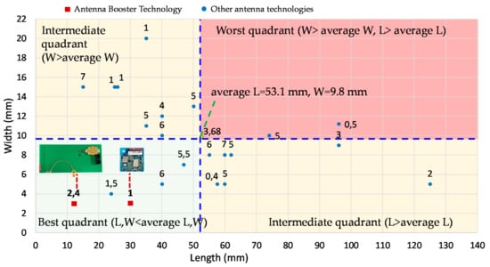
Figure 16.
Classification of several reconfigurable multiband antennas.
Regarding the active component for the matching network, not only were DTCs and SPNT switches used, but some solutions included PIN diodes to connect or disconnect one or more conductive parts of the antenna to obtain a multiband performance.
For comparison purposes, the two-antenna booster’s reconfiguration-based solutions presented in this paper were included in the plot. The one using an antenna booster of 12 mm × 3 mm × 2.4 mm, providing operation from 698 MHz to 960 MHz and from 1710 MHz to 2690 MHz, and a second one featuring an antenna booster of 30 mm × 3 mm × 1 mm for operation at 698–960 MHz and 1710–2170 MHz, as well as in GPS using the same reconfigurable matching circuit. Besides the lengths and widths, the antenna height was included in the plot with a number indicating heights in millimeters.
As is clearly shown in Figure 16, the antenna booster’s reconfiguration-based solutions were in the best quadrant, and furthermore, they were in the best location within that area; the one with a 2.4 mm height in particular was the best among all samples, featuring a small volume of only 86.4 mm3. In second place was the 30 mm × 3 mm × 1 mm antenna booster featuring a volume of 90 mm3. This solution had a smaller volume than the one having a 1.5 mm height, having a volume of 144 mm3. As a final remark, antenna booster technology features the smallest footprint and volume while providing performance across many frequencies within a 0.7–3 GHz range.
6. Conclusions
Two multiband reconfigurable antenna architectures for wireless devices using antenna boosters have been presented, having a small antenna booster size of less than 90 mm3 for operation at 698–960 MHz as well as 1710–2690 MHz, being the smallest volume among twenty antenna samples from the prior-art. Such multiband reconfigurability was achieved by combining digitally tunable capacitors and RF switches with antenna boosters. On one hand, the DTC provides reconfigurability thanks to a tunable capacitor that, when combined with a multiband matching network and an antenna booster, allows reconfiguration of the frequency bands. In other situations where changing a capacitor is not sufficient for providing enough freedom to tune the frequency bands, an architecture with RF switches, such as the one presented here, can be adopted. Both DTCs and RF switches use an interface than can be easily connected with most transceivers. Two solutions have been implemented: one with a DTC and an antenna booster of 86.4 mm3 in a reference board and another with two RF switches and an antenna booster of 90 mm3 in a cellular IoT device, showing competitive efficiency values for the wireless industry. These antenna booster architectures can be easily adopted in wireless devices because the antenna booster does not need geometry customization, since the multiband operation is adjusted by the design of the matching network, being a fast and easy design process. Finally, an antenna booster can simply be embedded due to its small size and off-the-shelf nature, resulting in attractive technology for the everything-connected world.
Author Contributions
J.A. and A.A. conceived the paper structure and, together with J.L.L. and O.M., led the development of the antenna booster part. J.T., E.R., and R.B. led the IoT device (Thingy:91) development, contributing to the RF switch section. R.G. contributed to the DTC section. All authors have read and agreed to the published version of the manuscript.
Funding
Part of this research was financed by the Spanish Ministry of Industry, Energy, and Tourism, belonging to the National Plan of Scientific Research, Development, and Technology Innovation 2015–2017 (Project Ref: TSI-100103-2015-39). It was also financed by the CDTI (Centro Desarrollo Tecnológico Industrial) of the Spanish Ministry of Science and Innovation in 2020–2021 (Project Ref: TIC-20200069).
Conflicts of Interest
The authors declare no conflict of interest.
References
- Anguera, J.; Andújar, A.; Huynh, M.C.; Orlenius, C.; Picher, C.; Puente, C. Advances in Antenna Technology for Wireless Handheld Devices. Int. J. Antennas Propag. 2013, 2013, 838364. [Google Scholar] [CrossRef]
- Zheng, M.; Wang, H.; Hao, Y. Internal Hexa-Band Folded Monopole/Dipole/Loop Antenna With Four Resonances for Mobile Device. IEEE Trans. Antennas Propag. 2012, 60, 2880–2885. [Google Scholar] [CrossRef]
- Kim, B.-N.; Park, S.-O.; Lee, J.-H.; Oh, J.-K.; Lee, K.-J.; Koo, G.-Y. Hepta-band planar inverted-F antenna with novel feed structure for wireless terminals. In Proceedings of the 2007 IEEE Antennas and Propagation Society International Symposium, Honolulu, HI, USA, 9–15 June 2007; pp. 1257–1260. [Google Scholar]
- Ban, Y.-L.; Qiang, Y.-F.; Chen, Z.; Kang, K.; Li, J.L.-W. Low-Profile Narrow-Frame Antenna for Seven-Band WWAN/LTE Smartphone Applications. IEEE Antennas Wirel. Propag. Lett. 2014, 13, 463–466. [Google Scholar] [CrossRef]
- Chen, Z.X.; Ban, Y.L.; Chen, Z.; Kang, K.; Li, J.L.W. Two-strip narrow-frame monopole antenna with a capacitor loaded for hepta-band smartphone applications. Prog. Electromagn. Res. 2014, 145, 31–38. [Google Scholar] [CrossRef]
- Ban, Y.-L.; Liu, C.-L.; Li, J.L.-W.; Li, R. Small-Size Wideband Monopole With Distributed Inductive Strip for Seven-Band WWAN/LTE Mobile Phone. IEEE Antennas Wirel. Propag. Lett. 2013, 12, 7–10. [Google Scholar] [CrossRef]
- Deng, C.; Li, Y.; Zhang, Z.; Feng, Z. A Novel Low-Profile Hepta-Band Handset Antenna Using Modes Controlling Method. IEEE Trans. Antennas Propag. 2014, 63, 799–804. [Google Scholar] [CrossRef]
- Wang, Y.; Du, Z. Wideband Monopole Antenna With Less Nonground Portion For Octa-Band WWAN/LTE Mobile Phones. IEEE Trans. Antennas Propag. 2016, 64, 383–388. [Google Scholar] [CrossRef]
- Huang, D.; Du, Z.; Wang, Y. An Octa-band Monopole Antenna With a Small Nonground Portion Height for LTE/WLAN Mobile Phones. IEEE Trans. Antennas Propag. 2016, 65, 878–882. [Google Scholar] [CrossRef]
- Wu, D.; Cheung, S.W.; Yuk, T.I. A Compact and Low-Profile Loop Antenna With Multiband Operation for Ultra-Thin Smartphones. IEEE Trans. Antennas Propag. 2015, 63, 2745–2750. [Google Scholar] [CrossRef]
- Xu, Z.-Q.; Zhou, Q.-Q.; Ban, Y.-L.; Ang, S.S. Hepta-Band Coupled-Fed Loop Antenna For LTE/WWAN Unbroken Metal-Rimmed Smartphone Applications. IEEE Antennas Wirel. Propag. Lett. 2017, 17, 311–314. [Google Scholar] [CrossRef]
- Anguera, J.; Andújar, A.; Puente, C. Antenna-Less Wireless: A Marriage Between Antenna and Microwave Engineering. Microw. J. 2017, 60, 22–36. [Google Scholar]
- Anguera, J.; Andújar, A.; Puente, C.; Mumbrú, J. Antennaless Wireless Device Capable of Operation in Multiple Frequency Regions. U.S. Patent 8,736,497, 4 August 2008. [Google Scholar]
- Andújar, A.; Anguera, J.; Puente, C. Ground Plane Boosters as a Compact Antenna Technology for Wireless Handheld Devices. IEEE Trans. Antennas Propag. 2011, 59, 1668–1677. [Google Scholar] [CrossRef]
- Anguera, J.; Andújar, A.; Puente, C. Wireless Handheld Devices, Radiation Systems and Manufacturing Methods. Patent CN 104508905 (B), 19 July 2013. [Google Scholar]
- Anguera, J.; Picher, C.; Bujalance, A.; Andújar, A. Ground plane booster antenna technology for smartphones and tablets. Microw. Opt. Technol. Lett. 2016, 58, 1289–1294. [Google Scholar] [CrossRef]
- Anguera, J.; Andújar, A.; Mestre, G.; Rahola, J.; Juntunen, J. Design of Multiband Antenna Systems for Wireless Devices Using Antenna Boosters. IEEE Microw. Mag. 2019, 20, 102–114. [Google Scholar] [CrossRef]
- De Mingo, J.; Valdovinos, A.; Crespo, A.; Navarro, D.; Garcia, P. An RF Electronically Controlled Impedance Tuning Network Design and Its Application to an Antenna Input Impedance Automatic Matching System. IEEE Trans. Microw. Theory Tech. 2004, 52, 489–497. [Google Scholar] [CrossRef]
- Yang, S.; Zhang, C.; Pan, H.K.; Fathy, A.E.; Nair, V.K. Frequency-Reconfigurable Antennas for Multiradio Wireless Platforms. IEEE Microw. Mag. 2009, 10, 66–83. [Google Scholar] [CrossRef]
- Chi, Y.-W.; Wong, K.-L. Quarter-Wavelength Printed Loop Antenna With an Internal Printed Matching Circuit for GSM/DCS/PCS/UMTS Operation in the Mobile Phone. IEEE Trans. Antennas Propag. 2009, 57, 2541–2547. [Google Scholar] [CrossRef]
- Iyer, V.; Makarov, S.N.; Harty, D.D.; Nekoogar, F.; Ludwig, R. A Lumped Circuit for Wideband Impedance Matching of a Non-Resonant, Short Dipole or Monopole Antenna. IEEE Trans. Antennas Propag. 2010, 58, 18–26. [Google Scholar] [CrossRef]
- Li, Y.; Zhang, Z.; Zheng, J.; Feng, Z.; Iskander, M.F. A Compact Hepta-Band Loop-Inverted F Reconfigurable Antenna for Mobile Phone. IEEE Trans. Antennas Propag. 2012, 60, 389–392. [Google Scholar] [CrossRef]
- Liu, Y.; Zhou, Y.-M.; Liu, G.-F.; Gong, S.-X. Heptaband Inverted-F Antenna for Metal-Rimmed Mobile Phone Applications. IEEE Antennas Wirel. Propag. Lett. 2015, 15, 996–999. [Google Scholar] [CrossRef]
- Xu, H.; Wang, H.; Gao, S.; Zhou, H.; Huang, Y.; Xu, Q.; Cheng, Y. A Compact and Low-Profile Loop Antenna With Six Resonant Modes for LTE Smartphone. IEEE Trans. Antennas Propag. 2016, 64, 3743–3751. [Google Scholar] [CrossRef]
- Asadallah, F.A.; Costantine, J.; Tawk, Y. A Multiband Compact Reconfigurable PIFA Based on Nested Slots. IEEE Antennas Wirel. Propag. Lett. 2018, 17, 331–334. [Google Scholar] [CrossRef]
- Chen, Y.; Martens, R.; Valkonen, R.; Manteuffel, D. Evaluation of adaptive impedance tuning for reducing the form factor of handset antenas. IEEE Trans. Antennas Propag. 2015, 63, 703–710. [Google Scholar] [CrossRef]
- Hoarau, C.; Corrao, N.; Arnould, J.D.; Ferrari, P.; Xavier, P. Complete design and measurement methodology for a tunable RF impedance-matching network. IEEE Trans. Microw. Theory Tech. 2008, 56, 2620–2627. [Google Scholar] [CrossRef]
- Chen, Y.; Manteuffel, D. A Tunable Decoupling and Matching Concept for Compact Mobile Terminal Antennas. IEEE Trans. Antennas Propag. 2017, 65, 1570–1578. [Google Scholar] [CrossRef]
- Ida, I.; Takada, J.-I.; Toda, T.; Oishi, Y. An adaptive impedance matching system and its application to mobile antennas. In Proceedings of the 2004 IEEE Region 10 Conference TENCON 2004, Chiang Mai, Thailand, 21–24 November 2004; pp. 543–546. [Google Scholar]
- Bahramzy, P.; Olesen, P.; Madsen, P.; Bojer, J.; del Barrio, S.C.; Tatomirescu, A.; Bundgaard, P.; Iii, A.S.M.; Pedersen, G.F. A Tunable RF Front-End With Narrowband Antennas for Mobile Devices. IEEE Trans. Microw. Theory Tech. 2015, 63, 3300–3310. [Google Scholar] [CrossRef]
- Anguera, J.; Toporcer, N.; Andújar, A. Slim Bar Boosters for Electronic Devices. U.S. Patent 9,960,478, 24 July 2014. [Google Scholar]
- Andújar, A.; Anguera, J.; Mateos, R. Multiband non-resonant antenna system with reduced ground clearance. In Proceedings of the 11th European Conference on Antennas and Propagation (EUCAP), Paris, France, 19–24 March 2017; pp. 3086–3089. [Google Scholar]
- Fano, R.M. Theoretical Limitations on the Broad-Band Matching of Arbitrary Impedances. J. Frankl. Inst. 1950, 249, 57–83. [Google Scholar] [CrossRef]
- Anguera, J.; Andújar, A.; Leiva, J.; Schepens, C.; Gaddi, R.; Kahng, S. Multiband antenna operation with a non-resonant element using a reconfigurable matching network. In Proceedings of the 12th European Conference on Antennas and Propagation (EuCAP 2018), London, UK, 9–13 April 2018. [Google Scholar]
- Tiggelman, M.P.J.; Reimann, K.; van Rijs, F.; Schmitz, J.; Hueting, R.J.E. On the Trade-Off Between Quality Factor and Tuning Ratio in Tunable High-Frequency Capacitors. IEEE Trans. Electron. Devices 2009, 56, 2128–2136. [Google Scholar] [CrossRef]
- Anguera, J.; Andújar, A. Wireless Device. U.S. Patent 10,122,403, 12 January 2016. [Google Scholar]
- Wang, D.; Wolf, R.; Joseph, A.; Botula, A.; Rabbeni, P.; Boenke, M.; Harame, D.; Dunn, J. High performance SOI RF switches for wireless applications. In Proceedings of the 10th IEEE International Conference on Solid-State and Integrated Circuit Technology, Shanghai, China, 1–4 November 2010; pp. 611–614. [Google Scholar]
- MIPI Alliance. MIPI White Paper: Enabling the IoT Opportunity; MIPI Alliance: Piscataway, NJ, USA, 2020. [Google Scholar]
- Anguera, J.; Andújar, A.; Leiva, J.L.; Cobo, Y.; Tønnessen, J.; Rindalsholt, E.; Brandsegg, R. Virtual Antenna™ Provides Mobile and GPS Connection in the Thingy:91 Cellular IoT Module; Fractus Antennas: Barcelona, Spain, 2020. [Google Scholar]
- Trinh, L.H.; Ferrero, F.; Lizzi, L.; Staraj, R.; Ribero, J.-M. Reconfigurable Antenna for Future Spectrum Reallocations in 5G Communications. IEEE Antennas Wirel. Propag. Lett. 2016, 15, 1297–1300. [Google Scholar] [CrossRef]
- Del Barrio, S.C.; Foroozanfard, E.; Morris, A.; Pedersen, G.F. Tunable Handset Antenna: Enhancing Efficiency on TV White Spaces. IEEE Trans. Antennas Propag. 2017, 65, 2106–2111. [Google Scholar] [CrossRef]
- Mun, B.; Jung, C.; Park, M.-J.; Lee, B. A Compact Frequency-Reconfigurable Multiband LTE MIMO Antenna for Laptop Applications. IEEE Antennas Wirel. Propag. Lett. 2014, 13, 1389–1392. [Google Scholar] [CrossRef]
- Ban, Y.-L.; Sun, S.-C.; Li, P.-P.; Li, J.L.-W.; Kang, K. Compact Eight-Band Frequency Reconfigurable Antenna for LTE/WWAN Tablet Computer Applications. IEEE Trans. Antennas Propag. 2014, 62, 471–475. [Google Scholar] [CrossRef]
- Ilvonen, J.; Valkonen, R.; Holopainen, J.; Viikari, V. Multiband Frequency Reconfigurable 4G Handset Antenna with MIMO Capability. Prog. Electromagn. Res. 2014, 148, 233–243. [Google Scholar] [CrossRef]
- Peng, C.-M.; Chen, I.-F.; Liu, C.-H. Multiband Printed Asymmetric Dipole Antenna for LTE/WLAN Applications. Int. J. Antennas Propag. 2013, 2013, 1–6. [Google Scholar] [CrossRef]
- Zhang, C.; Yang, S.; El-Ghazaly, S.; Fathy, A.; Nair, V. A Low-Profile Branched Monopole Laptop Reconfigurable Multiband Antenna for Wireless Applications. IEEE Antennas Wirel. Propag. Lett. 2008, 8, 216–219. [Google Scholar] [CrossRef]
- Hu, C.-L.; Huang, D.-L.; Kuo, H.-L.; Yang, C.-F.; Liao, C.-L.; Lin, S.-T. Compact Multibranch Inverted-F Antenna to be Embedded in a Laptop Computer for LTE/WWAN/IMT-E Applications. IEEE Antennas Wirel. Propag. Lett. 2010, 9, 838–841. [Google Scholar] [CrossRef]
- Li, H.; Xiong, J.; Yu, Y.; He, S. A Simple Compact Reconfigurable Slot Antenna With a Very Wide Tuning Range. IEEE Trans. Antennas Propag. 2010, 58, 3725–3728. [Google Scholar] [CrossRef]
- Li, Y.; Zhang, Z.; Zheng, J.; Feng, Z. Compact Heptaband Reconfigurable Loop Antenna for Mobile Handset. IEEE Antennas Wirel. Propag. Lett. 2011, 10, 1162–1165. [Google Scholar] [CrossRef]
- Ren, Y.-J. Ceramic Based Small LTE MIMO Handset Antenna. IEEE Trans. Antennas Propag. 2012, 61, 934–938. [Google Scholar] [CrossRef]
- Dioum, I.; Diallo, A.; Farssi, S.M.; Luxey, C. A Novel Compact Dual-Band LTE Antenna-System for MIMO Operation. IEEE Trans. Antennas Propag. 2014, 62, 2291–2296. [Google Scholar] [CrossRef]
- Singh, A.; Shamblin, J.; Jones, R.; Rowson, S.; Pajona, O.; Sron, S.T.; Floc’h, J.M.; Drissi, M.; Singh, A.; Jones, R. Compact active antenna for mobile devices supporting 4G LTE. In Proceedings of the 2014 Loughborough Antennas and Propagation Conference (LAPC), Loughborough, UK, 10–11 November 2014; pp. 525–529. [Google Scholar]
- Choi, M.; Wi, H.; Mun, B.; Yoon, Y.; Lee, H.; Lee, B. A Compact Frequency Reconfigurable Antenna for LTE Mobile Handset Applications. Int. J. Antennas Propag. 2015, 2015, 1–10. [Google Scholar] [CrossRef]
- Houret, T.; Lizzi, L.; Ferrero, F.; Danchesi, C.; Boudaud, S. DTC-Enabled Frequency-Tunable Inverted-F Antenna for IoT Applications. IEEE Antennas Wirel. Propag. Lett. 2019, 19, 307–311. [Google Scholar] [CrossRef]


Publisher’s Note: MDPI stays neutral with regard to jurisdictional claims in published maps and institutional affiliations. |
© 2021 by the authors. Licensee MDPI, Basel, Switzerland. This article is an open access article distributed under the terms and conditions of the Creative Commons Attribution (CC BY) license (http://creativecommons.org/licenses/by/4.0/).