Article

Conductive Electrifi and Nonconductive NinjaFlex Filaments based Flexible Microstrip Antenna for Changing Conformal Surface Applications

1
Department of Electrical and Computer Engineering, North Dakota State University, Fargo, ND 58102, USA
2
Department of Electrical Engineering, South Dakota School of Mines & Technology, Rapid City, SD 57701, USA
3
Department of Electrical Engineering and Computer Science, University of Toledo, Toledo, OH 43606, USA
4
Multi3D Inc., Cary, NC 27751, USA
*
Authors to whom correspondence should be addressed.
These authors contributed equally to this work.
Electronics 2021, 10(7), 821; https://doi.org/10.3390/electronics10070821
Submission received: 22 February 2021 / Revised: 16 March 2021 / Accepted: 23 March 2021 / Published: 30 March 2021
(This article belongs to the Special Issue Innovative Antenna Technologies and Applications)

Abstract

:
As the usage of wireless technology grows, it demands more complex architectures and conformal geometries, making the manufacturing of radio frequency (RF) systems challenging and expensive. The incorporation of emerging alternative manufacturing technologies, like additive manufacturing (AM), could consequently be a unique and cost-effective solution for flexible RF and microwave circuits and devices. This work presents manufacturing methodologies of 3D-printed conformal microstrip antennas made of a commercially available conductive filament, Electrifi, as the conductive trace on a commercially available nonconductive filament, NinjaFlex, as the substrate using the fused filament fabrication (FFF) method of AM technology. Additionally, a complete high frequency characterization of the prototyped antenna was studied and presented here through a comparative analysis between full-wave simulation and measurements in a fully calibrated anechoic chamber. The prototyped antenna measures 65.55 × 55.55 × 1.2 mm3 in size and the measured results show that the 3D-printed Electrifi based patch antenna achieved very good impedance matching at a resonant frequency of 2.4 GHz and a maximum antenna gain of −2.78 dBi. Finally, conformality performances of the developed antenna were demonstrated by placing the antenna prototype on five different cylindrical curved surfaces for possible implementation in flexible electronics, smart communications, and radar applications.

1. Introduction

The complex mechanical designs of modern communication systems often require that the associated antenna(s) be mounted on curved and conformal surfaces [1,2,3,4,5,6,7,8]. This may include placement of antennas on vehicles, aircrafts, or spacesuits, circular arrays [4,9], textile antennas, wireless body area networks (WBAN) [10,11,12,13], or unique composites for integrating the antenna into a geometry for load-bearing purposes [14]. Modern military aircraft would also benefit from the integration of conformal antennas for better signal intelligence. For example, there is a dire need to develop conformal antennas on aircraft such as the AC/MC-130Js to enable tactical operations by providing vehicles the potentiality to detect, locate, and target threats in a frequency domain not visualized when the vehicles were built [15]. Moreover, the conformal antennas provide a series of other advantages that planar antennas lack, such as increased receiver surface area, reduced aerodynamic drag of the antenna system, and reduction of overall antenna system size [16,17]. However, the complexities in the geometry of conformal antennas often pose significant challenges to designers and engineers in providing solutions that are both cost-effective and compact enough to fit in the backside of the curved or conformal surfaces. In short, the most compelling challenge is to come up with design and manufacturing methods for conformal antennas in a way that allows antenna properties to be predicted reliably.
To address the complexities and intricacies in manufacturing conformal antennas, researchers across the world have proposed a wide range of solutions in terms of materials, structures, and manufacturing processes. In [18], researchers presented a substrate integrated waveguide (SIW) conformal horn antenna using Rogers RT 5880 substrate on a conducting layer where a significant challenge remained in the presence of large conducting layers which caused the radiation patterns to tilt away from the cylindrical surface. Next, a conformal double exponentially tapered slot antenna (DETSA) on flexible liquid crystal polymer was proposed for ultra-wideband (UWB) applications using a standard photolithography fabrication process [19]. The researchers in [20] proposed E-textile conductors and polymer-ceramic composites as a solution for conformal lightweight antennas where the E-textile conductors were fabricated with single wall carbon nanotubes (SWNT) sputtered with silver for better conductivity. Next, a conformal coplanar waveguide (CPW) folded slot antenna was presented on a Kapton substrate for wearable networks and conformal sensors [21]. In [22], researchers demonstrated multilayer stretchable conductors (SCs) made of poly-dimethyl-siloxane (PDMS) substrate as a cost-effective alternative for realizing flexible and conformal antennas; however, it lacked the further investigation of the different layers and material configurations to improve the conductivity of the proposed multilayer SCs. A combination of laser micromachining and laser direct-write processes was introduced in [23] to develop conformal Global Positioning System (GPS) antennas to be integrated with air- and space-borne systems. Researchers have also successfully fabricated microstrip antennas on spherical surfaces using holographic photolithography [24]. However, photolithography is still a complex and expensive manufacturing process in general. As a conglomerate, these studies indicate the plethora of research avenues that could allow conformal antennas to be manufactured with a more ease.
Recently, additive manufacturing (AM) has revolutionized both the commercial and research industries by presenting different kinds of rapid prototyping techniques for realizing complex geometries and structures. Particularly, multiple research groups have reported various additive manufacturing methods for prototyping antennas such as triple-ridge leaky-wave antennas, quad-ridged horn antennas, ring-focus dual-reflector antennas, and dual-polarized leaky-wave antennas [25,26,27,28,29]. The inkjet printing technology of additive manufacturing was also adopted to develop conformal microstrip antennas using a piezoelectric nozzle array [30], a patch antenna emitter for wireless communication [31], and a 3D patch antenna with integrated polymer and metal [32]. Now, there are several kinds of AM methods available, but among them the fused filament fabrication (FFF) technique is the most popular in terms of simplicity, repeatability, and cost effectiveness. Fused filament fabrication uses cylindrically shaped molded filaments as the base materials along with single or multiple point(s) of extrusion in the form of benchtop 3D printers. The FFF manufacturing technique exploits the features of being scalable, programmable, and economic for printing both planar and nonplanar geometries and conformal shapes. Additionally, this method supports the ability of multimaterial printing that yields rapid manufacturing of high-frequency antennas and RF devices [33,34,35,36]. Now, a simple RF circuit can be visualized as a stack of alternating layers of materials: conductor and insulator, as shown in Figure 1a. A few studies have recently reported on using the FFF technique to additively manufacture substrate layers using polylactic acid (PLA) [37,38,39] and conductive layers using industrially available filaments with conductive characteristics [40,41,42,43] for microwave applications. Unlike the traditional ways involving various subtractive manufacturing methods to prototype RF circuits, additive technology has now unlocked new avenues for realizing flexible and complex geometries of RF circuits, including transmission lines, filters, and antennas [43,44,45,46] with a significantly lower cost and ease of manufacturing.
The authors have recently demonstrated in [47,48] about the possibility of prototyping such microwave transmission lines through the FFF method using conventional benchtop 3D printers. Specifically, an industrially available thermoplastic-based conductive filament [40], Electrifi, was first used to separately prototype the conductive traces of low-profile planar RF circuits. Then, the traces were fused to commercially available high-frequency substrate by means of an epoxy adhesive. The standard Electrifi filament can only be used to realize high frequency circuits up to a limited bandwidth of 3 GHz without sacrificing the linear phase response [47]. Next, a high-temperature based annealing was incorporated in the circuits made of Electrifi filament. The additional postprocessing step lead to an increase in the overall conductivity of the trace, resulting in a larger bandwidth of DC to 5 GHz, a significant increase of 67% [48]. A few researchers also reported in recent times on a parametric study using Electrifi filament for various RF applications, such as terrestrial Wi-Fi systems, DoD, WiMAX, and WLAN applications [49,50]. With such considerations, the authors in this paper have initially performed a characterization analysis of microwave propagation on a 50Ω transmission line (TL) made of Electrifi and NinjaFlex filaments as the conductive trace and substrate, respectively. Next, a planar microstrip patch antenna was realized using the Electrifi filament as the conductive top layer through FFF on a flexible substrate, manufactured using FFF and then incorporated with an Electrifi-made conductive top layer to report a 3D printed antenna for flexible applications, for the first time. Finally, conformality analysis of the 3D-printed Electrifi antenna was performed by placing the antenna on nonconducting cylindrical surfaces of five different radii (43 mm, 50 mm, 60 mm, 75 mm, and 88 mm).

2. Materials and Methods

2.1. RF Characterization Analysis of a 50 Ω TL Made of Electrifi and NinjaFlex Filaments

First, a 50 Ω microstrip TL, as shown in Figure 2, was fabricated using the Electrifi filament [40] as the top conducting layer on a square-shaped 3D-printed NinjaFlex substrate with commercially available 25.4 µm thick adhesive copper foil [51] as the bottom layer for reference (ground) plane. The Electrifi filament with 1.75 mm diameter was selected to be the appropriate candidate here due to this material’s (a) reported higher conductivity of 1.67 × 10⁴ S/m compared to other commercially available conductive filaments [41,42], (b) bandwidth from 1 GHz to 5 GHz with linear phase response [48], and (c) usage in realizing RF circuits recently reported by multiple groups of researchers [49,50]. A Creality CR-10 [52] 3D-printer, as shown in Figure 3a, was used to print the conductive Electrifi filament. Although the manufacturer-recommended printing temperature for this copper nanoparticle and thermoplastic-based Electrifi filament is between 140 °C and 160 °C, it was observed that the higher temperature range decreased the overall conductivity of the printed material [53]. An underlying protective layer of a blue paint tape was used on the printing bed as a separator while prototyping the conductive Electrifi trace to remove any chance of unnecessary adhesion between the printed conductive trace and the printing bed.
The electrical properties of the NinjaFlex material (εr = 2.6, tan δ = 0.07) were chosen as reported in [54]. The nonconductive substrate of the 50 Ω TL was additively manufactured by the FFF method with the commercially available NinjaFlex filament using a LulzBot Taz6 3D printer, as shown in Figure 3b. An underlying protective layer of uncoated polyetherimide (PEI) was used on the printing bed as a separator while prototyping the nonconductive NinjaFlex substrate to remove any chance of unnecessary adhesion between the printed substrate and the printing bed. Based on the reported electrical properties of NinjaFlex in [54], the thickness of the NinjaFlex substrate was determined to be 1.2 mm for industrial, scientific, and medical (ISM) band applications. Then, the 3D-printed conductive and nonconductive layers were laminated using a commercial adhesive spray [55] with a cure time of 24 h. Finally, the manufactured trace was electrically connected to a pair of SMA connectors (jack assembly, self-fixture end launch type) using an industrial silver epoxy (CAT. NO. 8330-19G) with a cure time of 24 h at 23 ℃. Table 1 represents the 3D printer settings in detail. The final prototype is shown in Figure 2b. The overall dimensions of the TL prototype are 50 × 50 × 1.2 mm3. The fabricated TL was also modeled using full-wave simulations in Ansys HFSS [56].
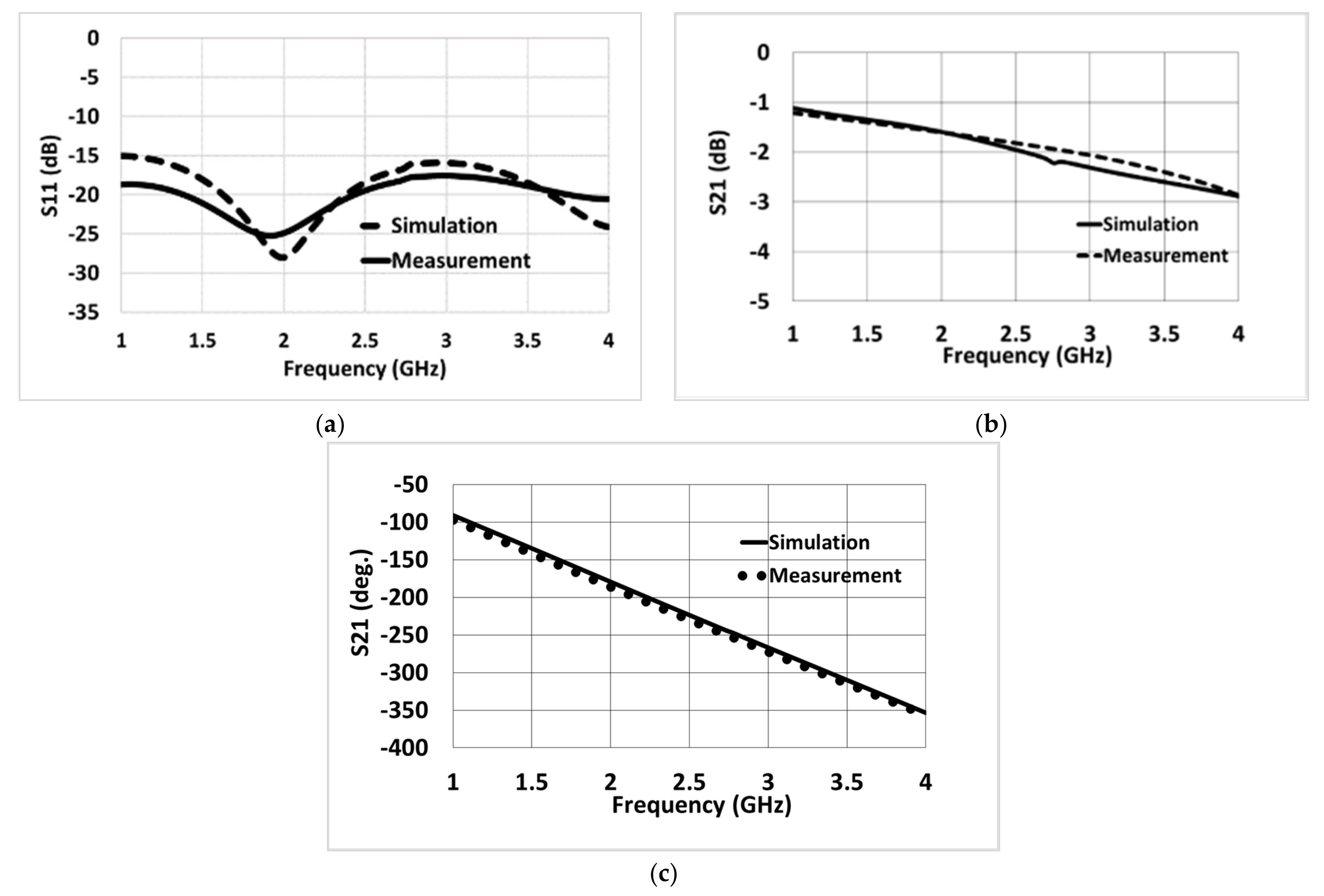
Next, the fabricated 50 Ω TL was characterized by using an Agilent ENA E5071C network analyzer. Followed by a two-port calibration method, the magnitude of the return loss (S11) and magnitude and phase of the transmission coefficient (S21) were recorded from 1 GHz to 4 GHz. For verification, the measured return loss and transmission coefficients were compared with the equivalent values obtained through full-wave simulations. Figure 4a shows the magnitude of return loss (S11). Figure 4b,c show the magnitude and the phase of transmission coefficient (S21), respectively. Overall, simulation and measurement data were in fair agreement.
Next, using the measured values of reflection coefficients (S11) and transmission coefficients (S21) in Figure 4, the attenuation constant (α) and phase constant (β) of the 50 Ω TL was evaluated. If l is the physical length and γ is the propagation constant of the TL, then using microwave transmission line theory, we can define the propagation function X where,
γ = α + j β = R + j w L G + j w C
and
X =   e γ l =   e j β l   e α l .
Now, if Z C is the characteristic impedance of the TL, Z 0 is the reference impedance of the measurement system, and Γ is the reflection coefficient of the TL, then by using the measured S11 and S21 of the TL, we can write
Γ   =   Z c   Z o / ( Z c +   Z o ) = Q   ±   Q 2 1
For a two-port matched network, where
Z c = R + j w L / G + j w C
and
Q =   S 11 2 +   S 21 2 +   1 / 2 S 11 .
Similarly, X can also be defined using the measured S11 and S21 of the TL:
X =   S 11 +   S 21 Γ / 1   S 11 +   S 21 .
Rearranging Equations (5) and (6) and substituting Γ in (3) yields
Γ     S 11 / ( S 11 2   S 21 2 + 1 ) .
Now, the intrinsic unit parameters of a traditional TL are defined as
  • R : resistance per unit length (Ω/m),
  • L : inductance per unit length (H/m)
  • C : capacitance per unit length (F/m), and
  • G : conductance per unit length (S/m).
Neglecting dielectric loss (tan δ = 0.07), and hence ignoring G and ratio R / ω L , which is very small, between 1 to 4 GHz ( f = ω / 2 π ), an approximation for γ yields
γ     R 2   C L + j ω L C =   R 2 Z C + j ω v p
where v p is the propagation velocity of the RF in the TL. Comparing real and imaginary parts in Equations (1) and (8) finally yields
α   R 2 Z C
and
β   ω v p
The derived attenuation constant and phase constant from the measured reflection and transmission coefficients of the 50 Ω Electrifi TL using Equations (9) and (10) were shown in Figure 5 from 1 GHz to 4 GHz. This information was later used in successfully modeling the Electrifi material for the full wave simulations while designing the antennas. A linear relation between the phase constant and frequency can be seen from Figure 5b where the equation of linearity was found as
β = 53.61 × f G H z + 0.27

2.2. Prototyping of the 3D-Printed Microstrip Patch Antenna on Flexible NinjaFlex Substrate

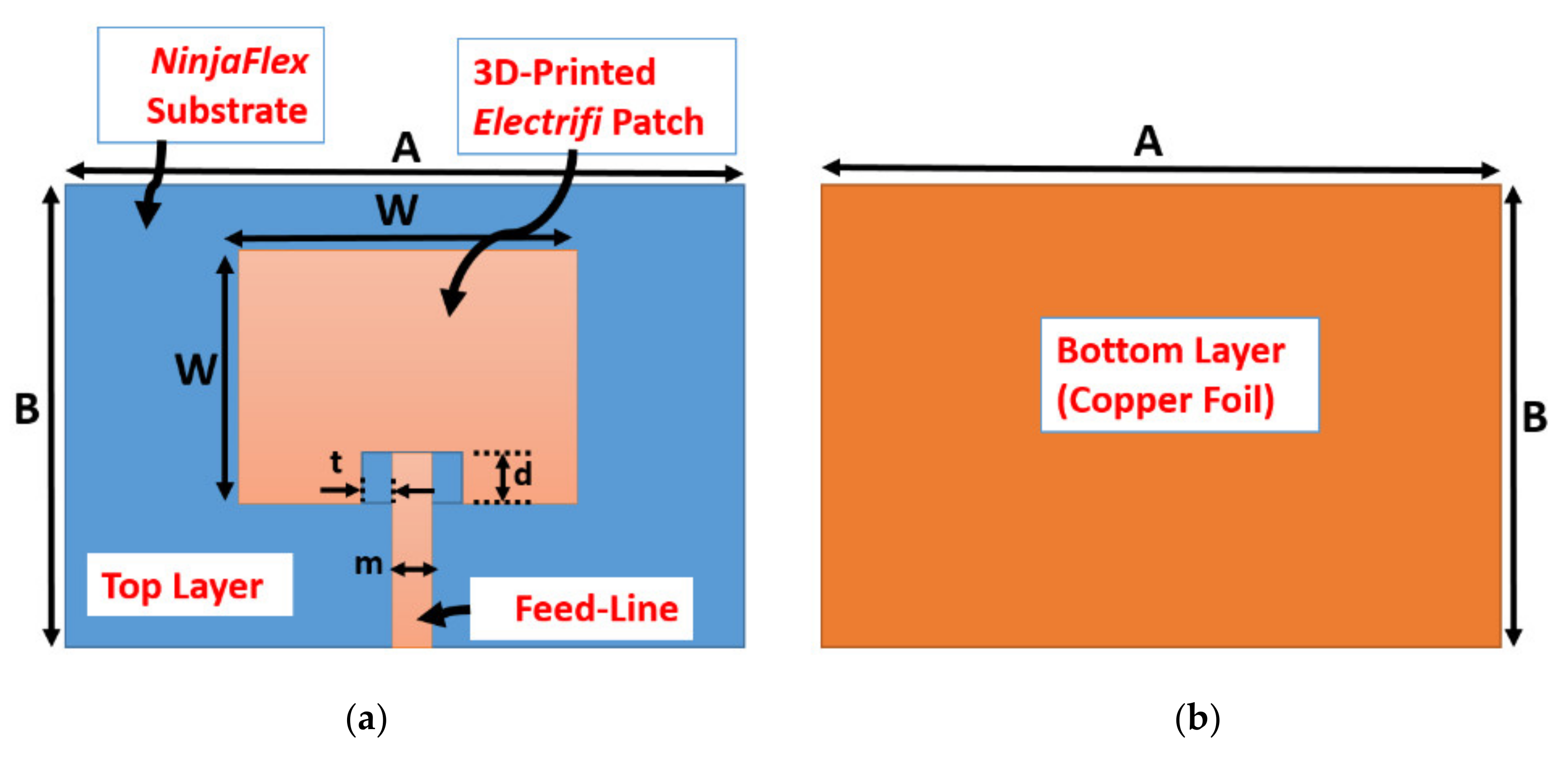
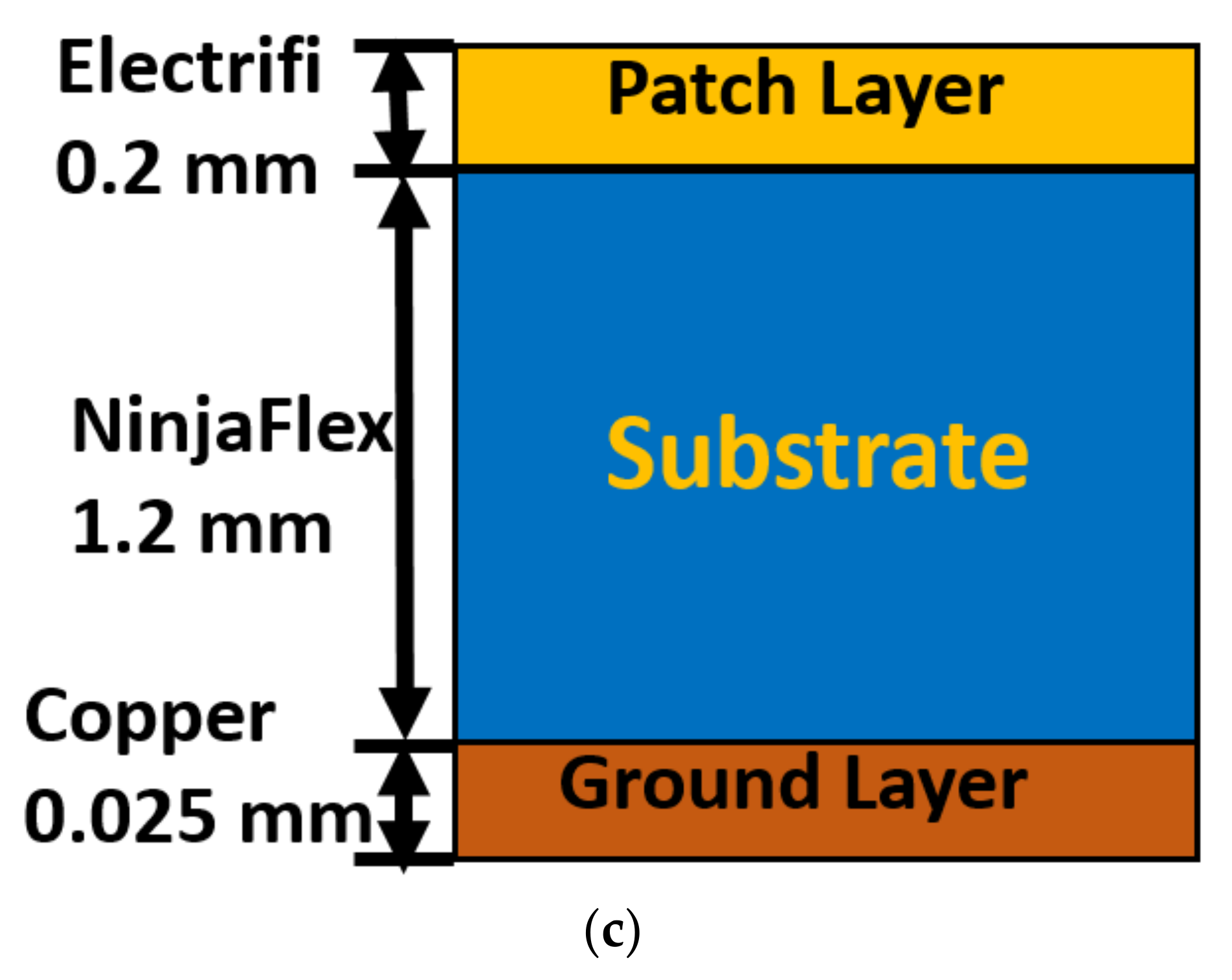
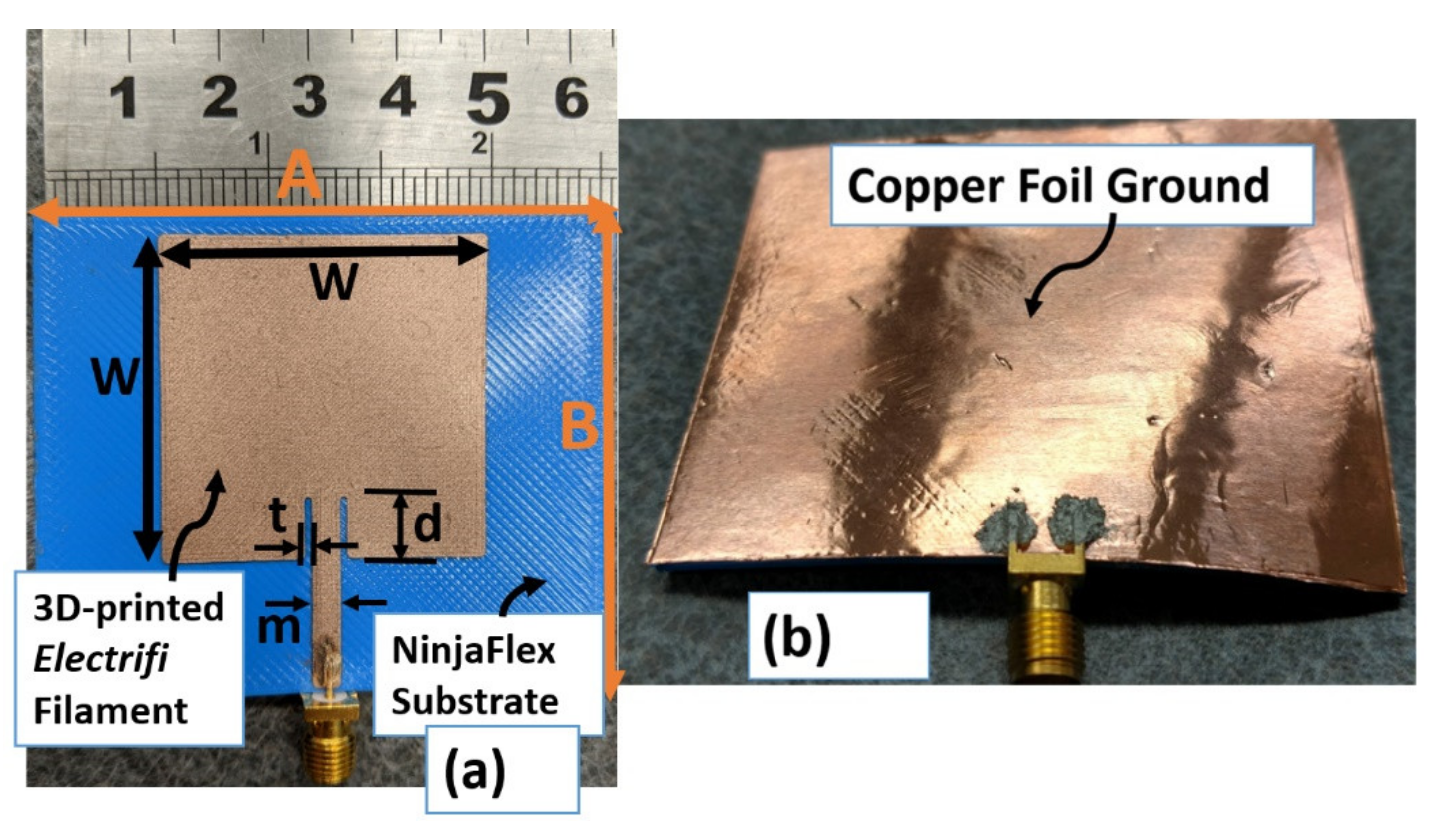
Based on the propagation analysis of the microstrip TL made of Electrifi and NinjaFlex filaments, a microstrip patch antenna was next realized using the improved version of commercially available Electrifi filament as the conductive top layer through the FFF method. All 3D printing settings were kept the same as mentioned in Section 2.1 while prototyping the 50 Ω TL. The thickness of the nonconductive NinjaFlex substrate was determined to be 1.2 mm for ISM band applications of the printed antenna at 2.5 GHz. The dimensions of the 3D-printed NinjaFlex substrate were 65.55 × 55.5 × 1.2 mm3. The conductive trace made of Electrifi filament and the nonconductive substrate made of NinjaFlex filament were separately 3D-printed by FFF technique using two different benchtop 3D printers as shown in Figure 3. These two layers were then laminated together using a commercial adhesive spray [55] using the similar process mentioned in Section 2.1. A commercially available 25.4 µm thick copper foil [51] was used as reference (ground) plane for the prototyped antenna. The complete geometry and the layer map of the 3D-printed microstrip patch antenna are shown in Figure 6. The complete dimensions of the 3D-printed microstrip patch antenna were A = 65.55, B = 55.5, W = 37, d = 7, t = 1, and m = 3, all in mm. Figure 7 shows the fabricated microstrip patch antenna prototype based on the conductive Electrifi filament on a 3D-printed flexible NinjaFlex substrate. It should be noted here that although multiple specimens including failed samples were printed during the manufacturing process, the printing method was improved through analyzing the failed samples, as reported in [53]. For the work reported in this paper, only one antenna prototype was chosen based on such adaptive printing method. The selected prototype was then used for all planar and nonplanar cylindrical conformal geometries with variable radii of curvatures.
Next, the fabricated prototype was modeled using a full wave simulation in Ansys HFSS [56]. Two major aspects in the full-wave model were the resistive loss of the 3D printed trace and the losses at the connections between the edge mounted SMA connector and the 3D-printed Electrifi patch feedline. The values of α and β obtained from Figure 5 at 2.5 GHz and the reported ohmic resistance value of the epoxy reported in [47] were used for such purposes. The effects of the SMA connector, silver epoxy, and adhesive spray were thus taken into consideration while modeling in HFSS.

2.2.1. Processing of the Conformal Surfaces for Testing

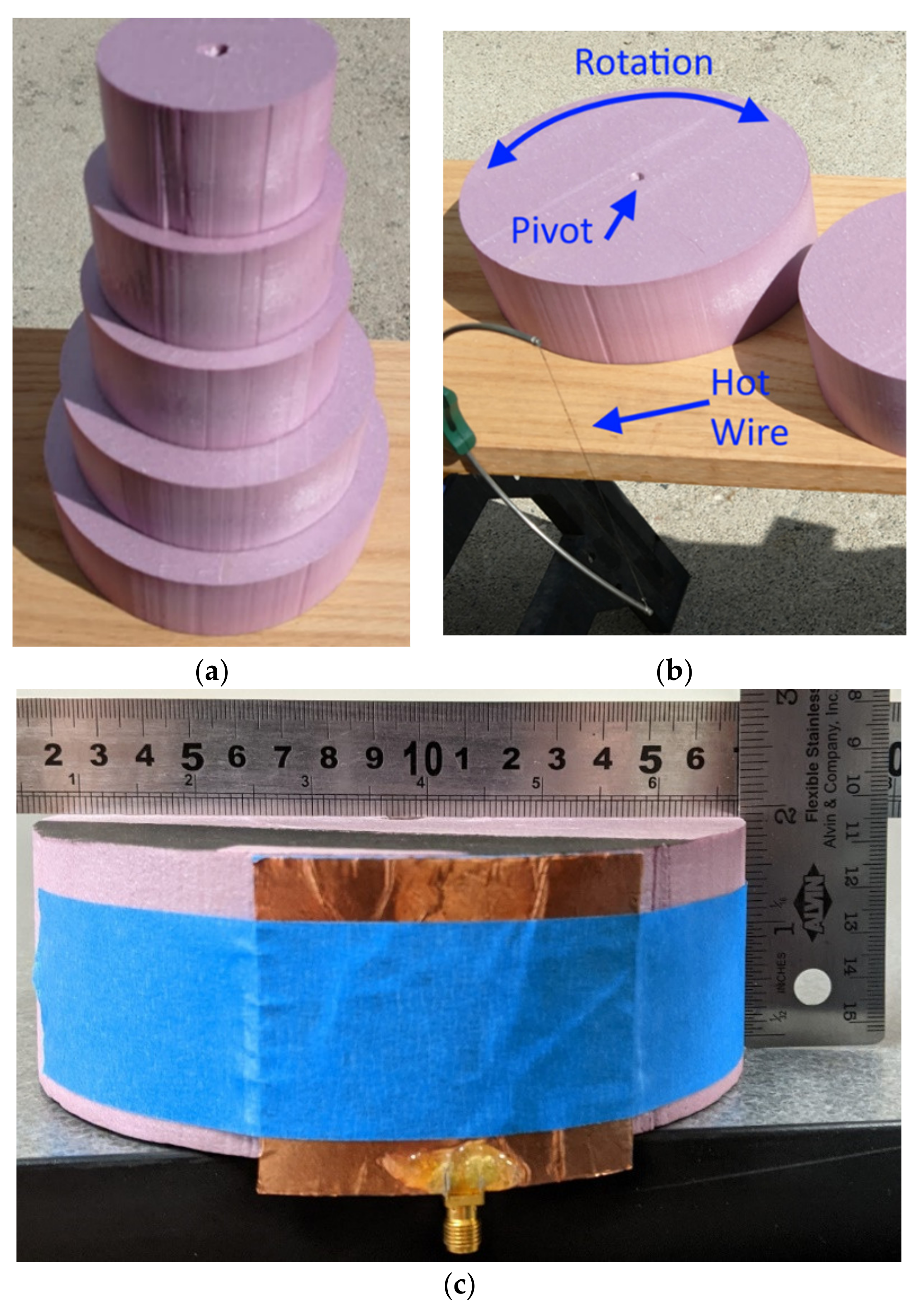
To test the developed 3D-printed conformal Electrifi antenna prototype under a variety of curvatures, support elements of various radii were fabricated, as shown in Figure 8a. Supports were fabricated as discs, which were cut from a 50.8 mm thick sheet of Owens Corning Foamular 150 rigid insulation board. This extruded polystyrene (XPS) material was chosen for its uniformly fine grain, closed-cell construction, rigidity, and low density. The low material density yields a dielectric value near that of free space [57]. The XPS material has a relative dielectric constant ( ε r ) in the range of 1.02 to 1.04 and a loss tangent ( t a n   δ ) in the range of 0.0018 to 0.002 [57,58]. Because the antenna would be affixed to the curved edge of each XPS disc, it was necessary to cut exceptionally clean and smooth curves. This was accomplished with a hot wire cutter mounted perpendicular to the plane of rotation for a rotational jig. By varying the distances between the hot wire and the jig’s pivot point, support discs of different radii were fabricated. First, the XPS material was cut into rough squares slightly larger than the desired support disc. Next, a pivot hole was pierced through the center of the XPS square. Then, the XPS sample was inserted into the jig and rotated, as shown in Figure 8b. As the sample was rotated, it passed through the hot wire cutter leaving a smooth edge of constant radius. The conformal antenna was affixed to each support disc in turn, and its performance was evaluated. The antenna was affixed with the radiating element inward (toward the center of the disc) and the ground plane outward (away from the disc) as shown in Figure 8c.

3. Results

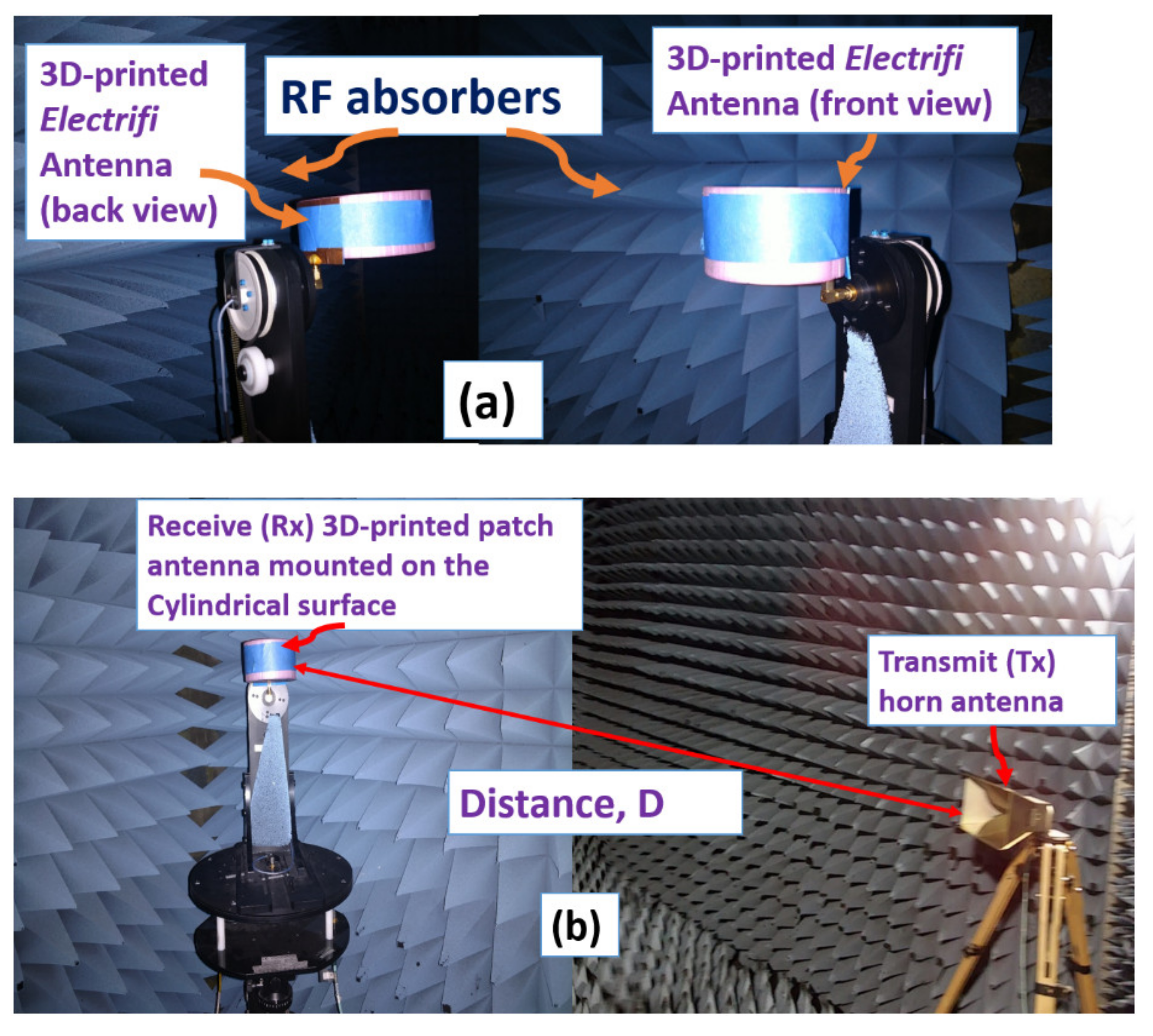
The performances of the 3D-printed conformal microstrip patch antenna were evaluated through the measurement of the return loss (S11), far-field radiation patterns, and gain for flat surface and five different cylindrical curved surfaces of radii 43, 50, 60, 75, and 88 mm, as described in Section 2.2.1. All measurements were performed using a Keysight E5071C ENA series network analyzer in a 10 × 10 × 10 ft3 fully calibrated anechoic chamber. The 3D-printed prototype was separately set on a rotating positioner for each cylindrical surface of different radius in the anechoic chamber, as shown in Figure 9a. Figure 9b shows the complete experimental setup in the anechoic chamber for gain and radiation pattern measurements. The prototypes (flat and cylindrical surfaces) were set as the receiver (RX) end with a distance of D = 3.14m from a transmitter horn antenna (TX) [59]. The experimental setup was composed of a network analyzer, two 12-feet long coaxial cables, one horn antenna as the transmitter (TX), and the 3D-printed patches as the receiver (RX). A detailed list of all equipment used is given in Table 2.

3.1. Reflection Coefficient (S11)

The reflection coefficients of the fabricated 3D-printed Electrifi antenna were measured by an E5071C vector network analyzer. The antenna prototype was placed on a flat surface and also was placed on five different cylindrical curved surfaces for ensuring conformal behavior of the fabricated antenna. All reflection coefficient measurements were validated by full-wave simulation in HFSS. Figure 10 presents the input reflection coefficient (S11) of the antenna prototype on a flat surface as well as cylindrical curved surfaces of 43, 50, 60, 75, and 88 mm, respectively. The magnitudes of S11 for all cases were well below −10 dB, and both the measured and simulation results were in good agreement. The measured resonant frequency was recorded to be marginally shifted for all cases. This was expected due to a little shifted value from nonunity of relative dielectric constant of the supported conformal structures (polystyrene) at the resonant frequency [57] and limited accuracy, precision, and resolution of the prototypes manufactured by the FFF technique which might lead to incorporate intrinsic manufacturing errors [60]. The comparison between measured reflection coefficients on a flat surface and five different cylindrical curved surfaces are presented in Figure 11. No significant changes in the measured resonance frequencies were observed while the prototyped antenna was placed on five different cylindrical curved surfaces. However, the measured return loss marginally improved while the antenna conformed from planar (i.e., flat) orientation to any nonplanar (i.e., cylindrical) orientation, which was due to the negligible parasitic effect of the cylindrical polystyrene support structure that was used for all nonplanar measurements of the antenna, as shown in Figure 9.

3.2. Description of Radiation Patterns

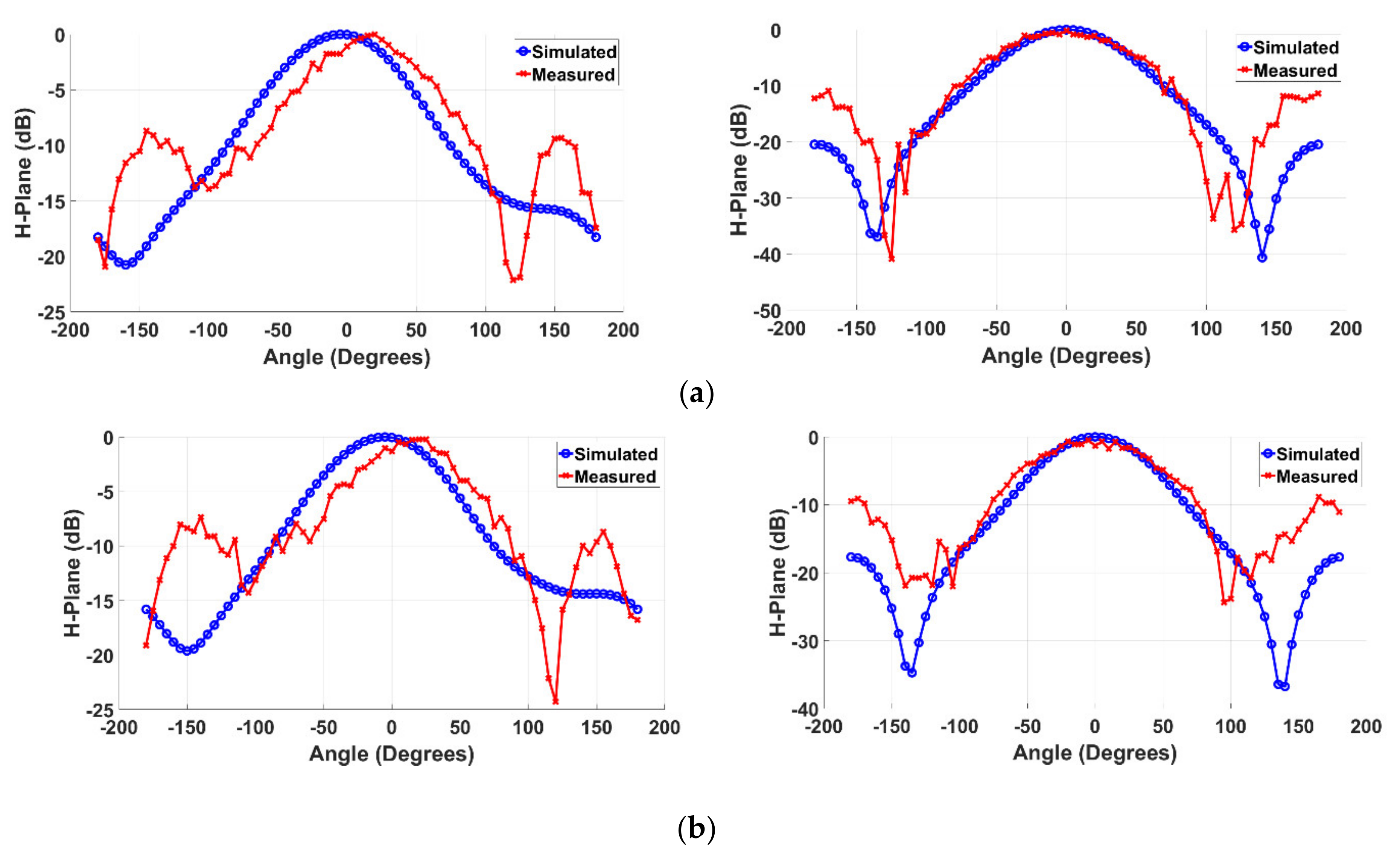
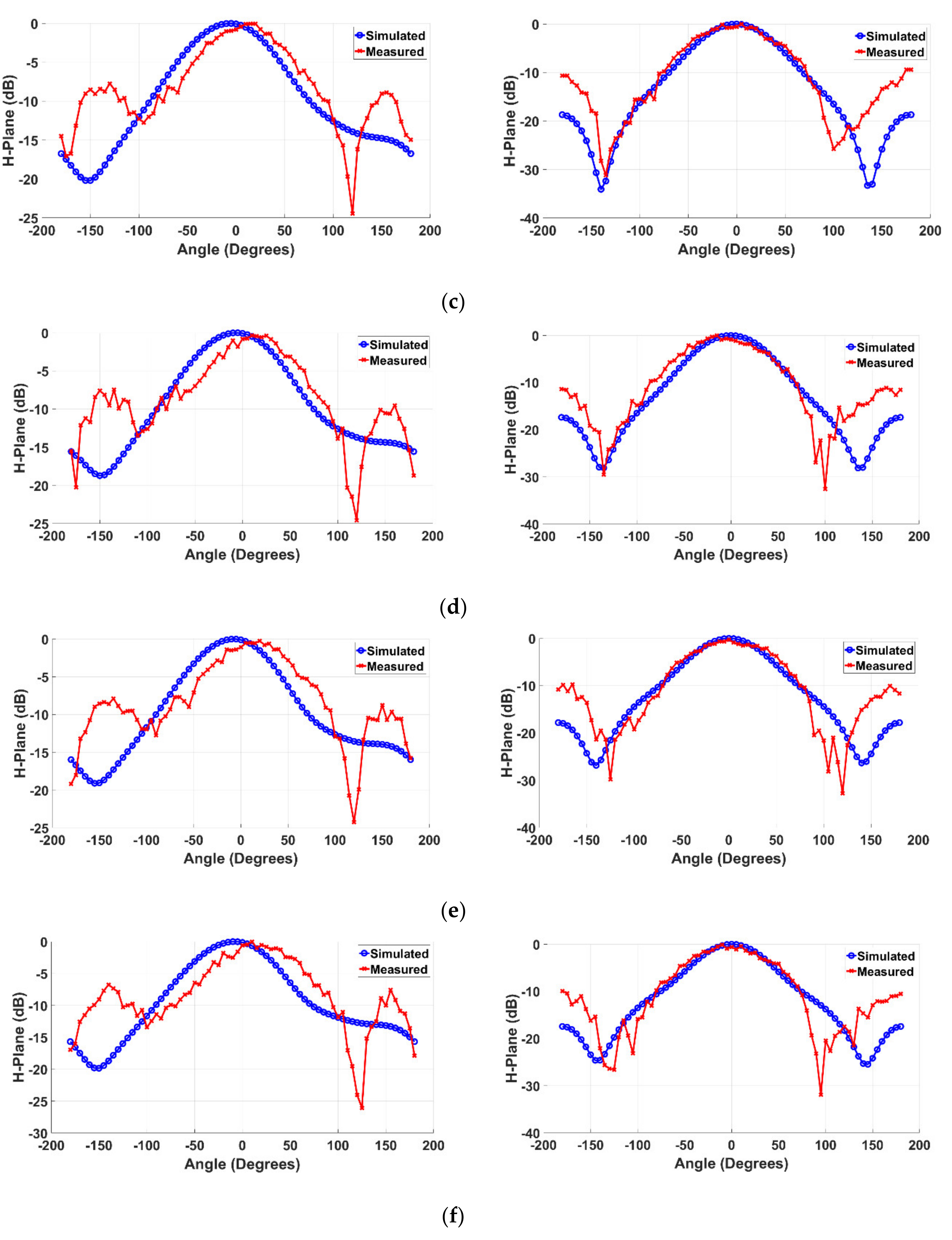
Figure 12 depicts the measured and simulated radiation characteristics of the 3D-printed Electrifi flexible antenna on a flexible NinjaFlex substrate at 2.4 GHz on the flat surface and on cylindrical curved surfaces of radii 88, 75, 60, 50, and 43 mm, respectively in two principal planes, E-plane (y-z) and H-plane (x-z). Measured E- and H-planes for all cases are in fair agreement with full-wave simulations in HFSS. Small discrepancies can be attributed to the imperfections of the measurement feeding cables and minor misalignments of the receiver and transmitter antennas in the anechoic chamber.

3.3. Analysis of Experimental Gain

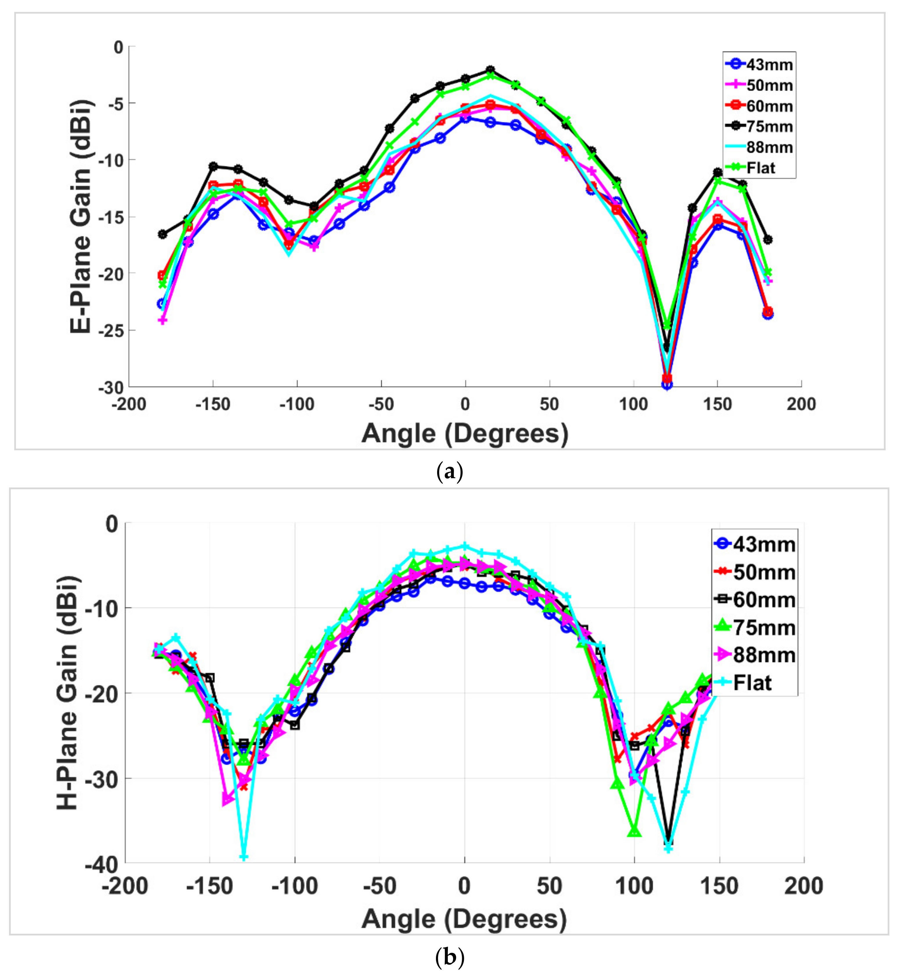
Comparisons between the measured gains of the 3D-printed Electrifi microstrip patch antenna prototype in both the principal E- and H-planes at a frequency of 2.4 GHz under different bending conditions are shown in Figure 13. During the gain measurements, a high degree of dimensional stability and polarization purity were retained. The highest measured gain of the 3D-printed Electrifi antenna was −2.78 dBi in the H-plane at 2.4 GHz, as shown in Figure 13b, and −2.87 dBi in the E-plane at 2.4 GHz, as shown in Figure 13a. This lower gain of the prototype was expected due to the use of lossy NinjaFlex material as the substrate.

3.4. Determination of Surface Current Distribution

Finally, the simulated surface current distributions of the 3D-printed microstrip patch antenna at 2.4 GHz is presented in Figure 14. The current distributions were simulated in a finite element method solver, HFSS, when the 3D-printed antenna was flat as well as mounted on cylindrical curved surfaces of radii 88, 75, 60, 50, and 43 mm. It was observed that when the antenna was flat, the current density was maximum at the center. As the curvature of the cylindrical surface increased (or the radius of the cylindrical surface decreased), the current density distributed more towards the edges of the 3D-printed microstrip patch antenna rather than the center. In the contrast, the current density was distributed more towards the center when the antenna moved towards a flat position, i.e., the curvature of the cylindrical surface decreased (or the radius of the cylindrical surface increased).
Furthermore, it should be noted here that a variation of 3.43 dB was observed in the E-plane gain under different bending conditions, while a variation of 4.34 dB was observed in the H-plane gain at a frequency of 2.4 GHz, as shown in Figure 13. Despite the improved return loss profile (Figure 11) for nonplanar orientations of the antenna, such significant degradations in the measured gain of the antenna (Figure 13) under different radii of curvature were anticipated. As Figure 14a through 14f suggest, the current density on the patch tended to be distributed more towards the edges as the radius of the cylindrical surface decreased. Hence, the gain severely dropped as the antenna conformed to much smaller radii of curvature.

4. Discussion

Overall, this work is summarized as below:
  • A 50 Ω TL model was realized using an improved version of conductive Electrifi filament on 3D-printed NinjaFlex substrate, and later, the TL model was characterized to analyze RF propagation of the Electrifi filament showing attenuation and phase constant.
  • The propagation constant ( γ = α + j β ) of the Electrifi filament from Section 2 was used in full-wave model to model a microstrip patch antenna using the fused filament fabrication (FFF) method of additive manufacturing on a flexible 3D-printed NinjaFlex substrate for conformal applications. This method introduced a low-cost and easy-to-fabricate 3D-printing method compared to existing solutions and methods for realizing complex and conformal RF structures.
  • The fabricated 3D-printed Electrifi antenna was shown to have extraordinary flexibility and conformality performances. The conformal experimentation was performed through mounting the 3D-printed Electrifi antenna prototype on curved cylindrical surfaces of five different radii.
  • The reflection coefficients, radiation patterns, and gains in Figure 10, Figure 11 and Figure 12 showed that the 3D-printed Electrifi antenna performed very well except for small discrepancies under different bending conditions, which would make it a very suitable candidate for various conformal applications.
  • Due to the use of NinjaFlex material as the substrate, low gain was observed, in future different flexible substrates with lower loss might be used for better gain performance.
  • The simulated current density results in Figure 14 showed that the current density remained in the center when the antenna geometry was flat, and the current tended to be more distributed towards the edges from the center as the curvature of the conformal surfaces increased.

5. Conclusions

To conclude, this paper reported a 3D-printed microstrip patch antenna based on an improved version of commercially available conductive Electrifi and nonconductive NinjaFlex filaments by utilizing the unique fused filament fabrication (FFF) method of AM technology. This paper additionally presented high-frequency characterization of the developed prototype in a fully calibrated anechoic chamber for potential flexible and wearable electronics applications in the ISM bands. The flexible NinjaFlex substrate was used, which was also 3D-printed. The fabricated prototype measured 65.55 × 55.55 × 1.2 mm3 in size. The measured results showed that the 3D-printed microstrip flexible antenna achieved a very good impedance matching at a resonant frequency of 2.4 GHz and a maximum antenna gain of −2.78 dBi, which made the prototype suitable for applications like Wi-Fi, WiMAX, and microwave satellite communications. Additionally, to test the developed 3D-printed conformal microstrip antenna prototype under a variety of curvatures, the fabricated antenna was mounted on five different cylindrical curved surfaces of radii of 88, 75, 60, 50, and 43 mm, respectively. The 3D-printed Electrifi antenna demonstrated extraordinary conformal performances under different curvatures in terms of measured reflection coefficients, radiation patterns, and gains. This also showed that unlike rigid copper traces which have a natural tendency to fail for flexible applications, the conductive Electrifi filament could be a viable alternative, and is a very flexible, cost-effective and easy-to-manufacture composite material with the current advent of additive manufacturing. The developed prototype was fully modeled in a full-wave 3D electromagnetic (EM) simulation software Ansys HFSS based on finite element method (FEM). Overall, the agreement between the measurement and the full-wave simulation was observed to be very reasonable, making the reported 3D-printed microstrip flexible antenna a worthy candidate for conformal surface applications.

Author Contributions

Conceptualization, D.M. and S.R.; methodology, D.M., S.R., and R.S.; validation, D.M., R.S., S.R., E.B., A.A., H.W., and K.S.K.; formal analysis, D.M., S.R., R.S., E.B., A.A., H.W., and K.S.K.; writing—original draft preparation, D.M., S.R.; writing—review and editing, B.D.B., A.A.; E.B.; R.S., S.Y.; supervision, S.R., B.D.B.; All authors have read and agreed to the published version of the manuscript.

Funding

This research is based upon work supported by the National Science Foundation under Grant No. 1849206, National Aeronautics and Space Administration (NASA) under Grant No. 80NSSC18M0022, and South Dakota Board of Regents Competitive Research Grant Program FY21. D.M. would like to acknowledge NDSU College of Graduate and Interdisciplinary Studies Doctoral Dissertation Fellowship for partly supporting this research.

Acknowledgments

The authors would like to thank Jeffery Erickson in the Department of Electrical and Computer Engineering at North Dakota State University, Fargo, ND Venkataramana Gadhamshetty in the Civil and Environmental Engineering at South Dakota School of Mines & Technology, Rapid City, SD for their help and insightful discussions during the development of the prototypes.

Conflicts of Interest

The authors declare no conflict of interest.

References

  1. O’Donovan, P.L.; Rudge, A.W. Adaptive control of a flexible linear array. Electron. Lett. 1973, 9, 121–122. [Google Scholar] [CrossRef]
  2. Chung, D.J.; Bhattacharya, S.K.; Ponchak, G.E.; Papapolymerou, J. An 8×8 Lightweight Flexible Multilayer Antenna array. In Proceedings of the 2009 IEEE Antennas and Propagation Society International Symposium, Charleston, SC, USA, 1–5 June 2009; pp. 1–4. [Google Scholar]
  3. Hansen, R.C. Phased Array Antennas; Wiley: New York, NY, USA, 1998. [Google Scholar]
  4. Haupt, R.L. Antenna Arrays: A Computational Approach; Wiley: Hoboken, NJ, USA, 2010. [Google Scholar]
  5. Roy, S.; Sajal, S.; Braaten, B.D. A phase correction technique based on spatial movements of antennas in real-time for designing self-adapting conformal array antennas. Microw. Opt. Technol. Lett. 2017, 59, 3002–3010. [Google Scholar] [CrossRef]
  6. Guo, J.L.; Li, J.Y. Pattern Synthesis of Conformal Array Antenna in the Presence of Platform Using Differential Evolution Algorithm. IEEE Trans. Antennas Propag. 2009, 57, 2615–2621. [Google Scholar]
  7. Zhu, S.; Langley, R. Dual-Band Wearable Textile Antenna on an EBG Substrate. IEEE Trans. Antennas Propag. 2009, 57, 926–935. [Google Scholar] [CrossRef] [Green Version]
  8. Wincza, K.; Gruszczynski, S. Influence of curvature Radius on Radiation Patterns in Multibeam Conformal Antennas. In Proceedings of the 36th European Microwave Conference, Manchester, UK, 10–15 September 2006; pp. 1410–1413. [Google Scholar]
  9. Josefsson, L.; Persson, P. Conformal Array Antenna Theory and Design; Wiley: Hoboken, NJ, USA, 2006. [Google Scholar]
  10. Klemm, M.; Troester, G. Textile UWB Antennas for Wireless Body Area Networks. IEEE Trans. Antennas Propag. 2006, 54, 3192–3197. [Google Scholar] [CrossRef] [Green Version]
  11. Kennedy, T.F.; Fink, P.W.; Chu, A.W.; Champagne, N.J.; Lin, G.Y.; Khayat, M.A. Body-Worn E-Textile Antennas: The Good, the Low Mass, the Conformal. IEEE Trans. Antennas Propag. 2009, 57, 910–918. [Google Scholar] [CrossRef]
  12. Salonen, P.; Rahmat-Samii, Y.; Schaffrath, M.; Kivikoski, M. Effect of Textile Materials on Wearable Antenna Performance: A Case Study of GPS Antennas. Proc. IEEE Int. Symp. Antennas Propag. Soc. 2004, 1, 459–462. [Google Scholar]
  13. Psychodakis, D.; Lee, G.Y.; Chen, C.C.; Volakis, J.L. Estimating Diversity for Body-Worn Antennas. In Proceedings of the 3rd European Conference on Antennas and Propagation (EuCAP), Berlin, Germany, 23–27 March 2009. [Google Scholar]
  14. Callus, P.J. Conformal Load-Bearing Antenna Structure for Australian Defense Force Aircraft; DSTO Platforms Sciences Laboratory: Victoria, Australia, 2007. [Google Scholar]
  15. Sbir.gov. Available online: https://www.sbir.gov/content/conformal-antennas-improved-signal-intelligence-0 (accessed on 1 November 2020).
  16. Liu, Y.; Yang, H.; Jin, Z.; Zhao, F.; Zhu, J. A Multibeam Cylindrically Conformal Slot Array Antenna Based on a Modified Rotman Lens. IEEE Tans. Antennas Propag. 2018, 66, 3441–3452. [Google Scholar] [CrossRef]
  17. Budhu, J.; Rahmat-Samii, Y.; Hodges, R.; Hofmann, U.C.; Ruffatto, D.F.; Carpenter, K. Three-Dimensionally Printed, Shaped, Engineered Material Inhomogenous Lens Antenna for Next-Generation Spaceborne Weather Radar Systems. IEEE Antennas Wirel. Propag. Lett. 2018, 17, 2080–2084. [Google Scholar] [CrossRef]
  18. Zhao, Y.; Shen, Z.; Wu, W. Conformal SIW H-Plane Horn Antenna on a Conducting Cylinder. IEEE Antennas Wirel. Propag. Lett. 2015, 14, 1271–1274. [Google Scholar] [CrossRef]
  19. Nikolaou, S.; Ponchak, G.E.; Papapolymerou, J.; Tentzeris, M.M. Conformal Double Exponentially Tapered Slot Antenna (DETSA) on LCP for UWB Applications. IEEE Trans. Antennas Propag. 2006, 54, 1663–1669. [Google Scholar] [CrossRef]
  20. Bayram, Y.; Zhou, Y.; Shim, B.S.; Xu, S.; Zhu, J.; Kotov, N.A.; Volakis, J.L. E-TextileConductors and Polymer Composites for Conformal Lightweight Antennas. IEEE Trans. Antennas Propag. 2010, 58, 2732–2736. [Google Scholar] [CrossRef]
  21. Aziz, M.A.; Roy, S.; Berge, L.A.; Ullah, I.; Braaten, B.D. A Conformal CPW Folded Slot Antenna Array Printed on a Kapton Substrate. In Proceedings of the European Microwave Conference, Prague, Czech Republic, 26–30 March 2012. [Google Scholar]
  22. Liyakath, R.A.; Takshi, A.; Mumcu, G. Multilayer Stretchable Conductors on Polymer Substrates for Conformal and Reconfigurable Antennas. IEEE Antennas Wirel. Propag Lett. 2013, 12, 603–606. [Google Scholar] [CrossRef]
  23. Auyeung, R.C.Y.; Nurnberger, M.W.; Wendland, D.J.; Pique, A.; Arnold, A.R.; Schuette, L.C. Laser Fabrication of GPS Conformal Antennas. In Proceedings of the Photon Processing in Microelectronics and Photonics III, San Jose, CA, USA, 26–29 January 2004. [Google Scholar]
  24. Toriz-Garcia, J.J.; Cowling, J.J.; Williams, G.L.; Bai, Q.; Seed, N.L.; Tennant, A.; McWilliam, R.; Purvis, A.; Soulard, F.B.; Ivey, P.A. Fabrication of a 3D Electrically Small Antenna Using Holographic Photolithography. J. Micromech. Microeng. 2013, 23, 055010. [Google Scholar] [CrossRef]
  25. Dorlé, A.; Gillard, R.; Menargues, E.; Vorst, M.V.D.; Rijk, E.D.; Martín-Iglesias, P.; Garcia- Vigueras, M. Additive Manufacturing of Modulated Triple-Ridge Leaky-Wave Antenna. IEEE Antennas Wirel. Propag. Lett. 2018, 17, 2123–2127. [Google Scholar] [CrossRef]
  26. Dimitriadis, A.I.; Debogović, T.; Costa, J.R.; Fernandes, C.A.; Mosig, J.R. Polymer-Based Additive Manufacturing of High-Performance Waveguide and Antenna Components. Proc. IEEE 2017, 105, 668–676. [Google Scholar] [CrossRef]
  27. Silva, J.S.; García-Vigueras, M.; Debogović, T.; Costa, J.R.; Fernandes, C.A.; Mosig, J.R. Sterolithography-Based Antennas for Satellite Communications in Ka-Band. Proc. IEEE 2017, 105, 655–667. [Google Scholar] [CrossRef]
  28. Vorst, M.V.D.; Gumpinger, J. Applicability of 3D Printing Techniques for Compact Ku-Band Medium/High-Gain Antennas. In Proceedings of the 10th European Conference on Antennas and Propagation (EuCAP), Davos, Switzerland, 10–15 April 2016; pp. 1–4. [Google Scholar]
  29. Garcia- Vigueras, M.; Menargues, E.; Debogović, T.; Rijk, E.D.; Mosig, J.R. Cost-Effective Dual-Polarized Leaky-Wave antennas Enabled by Three-Dimensional Printing. IET Microw. Antennas Propag. 2017, 11, 1985–1991. [Google Scholar] [CrossRef]
  30. Li, Z.; Huang, J.; Yang, Y.; Yang, S.; Zhang, J.; Yuan, P.; Zhang, J. Additive Manufacturing of Conformal Microstrip Antenna Using Piezoelectric Nozzle Array. Appl. Sci. 2020, 10, 3082. [Google Scholar] [CrossRef]
  31. Goh, G.L.; Ma, J.; Chua, K.L.; Shweta, A.; Yeong, W.Y.; Zhang, Y.P. Inkjet-printed patch antenna emitter for wireless communication application. Virtual Phys. Prototyp. 2016, 11, 289–294. [Google Scholar] [CrossRef]
  32. McKerricher, G.; Titterington, D.; Shamim, A. A fully inkjet-printed 3-D honeycomb-inspired patch antenna. IEEE Antennas Wirel. Propag. Lett. 2015, 15, 544–547. [Google Scholar] [CrossRef] [Green Version]
  33. Menéndez, L.G.; Kim, O.S.; Persson, F.; Nielsen, M.; Breinbjerg, O. 3D Printed 20/30-GHz Dual-Band Offset Stepped-Reflector Antenna. In Proceedings of the 2015 9th European Conference on Antennas and Propagationc (EuCAP), Libson, Portugal, 12–17 April 2015; pp. 1–2. [Google Scholar]
  34. Shang, X.; Penchev, P.; Guo, C.; Lancaster, M.J.; Dimov, S.; Dong, Y.; Favre, M.; Billod, M.; Rijk, E.D. W-Band Waveguide Filters Fabricated by Laser Micromachining and 3D Printing. IEEE Trans. Microw. Theor. Techniq. 2016, 64, 2572–2580. [Google Scholar] [CrossRef]
  35. Johnson, K.; Zemba, M.; Conner, B.P.; Walker, J.; Burden, E.; Rogers, K.; Cwiok, K.R.; Macdonald, E.; Cortes, P. Digital Manufacturing of Pathologically-Complex 3D Printed Antennas. IEEE Access. 2019, 7, 39378–39389. [Google Scholar] [CrossRef]
  36. Zhang, S. Three-Dimensional Printed Millimetre Wave Dielectric Resonator Reflectarray. IET Microw. Antennas Propag. 2017, 11, 2005–2009. [Google Scholar] [CrossRef] [Green Version]
  37. Piekarz, I.; Sorocki, J.; Slomian, I.; Wincza, K.; Gruszczynski, S. Experimental Verification of 3D Printed Low-Conductivity Graphene-Enhanced PLA Absorbers for Back Lobe Suppression in Aperture-Coupled Antennas. In Proceedings of the 2018 IEEE-APS Topical Conference on Antennas and Propagation in Wireless Communications (APWC), Cartenga des Indias, Colombia, 10–14 September 2018; pp. 780–782. [Google Scholar]
  38. Li, Y.; Ge, L.; Wang, J.; Da, S.; Cao, D.; Wang, J.; Liu, Y. 3D Printed High-Gain Wideband Waveguide Fed Horn Antenna Arrays for Millimeter-Wave Applications. IEEE Trans. Antennas Propag. 2019, 67, 2868–2877. [Google Scholar] [CrossRef]
  39. Mirzaee, M.; Noghanian, S. High Frequency Characterization of Wood-Fill PLA for Antenna Additive Manufacturing Application. Elec. Lett. 2016, 52, 1656–1658. [Google Scholar] [CrossRef]
  40. Electrifi Conductive Filament, multi3dllc. Available online: https://www.multi3dllc.com/product/Electrifi/ (accessed on 24 January 2021).
  41. BlackMagic3D. Available online: https://www.blackmagic3d.com/ (accessed on 30 June 2020).
  42. Proto-Pasta. Available online: https://www.proto-pasta.com/ (accessed on 30 June 2020).
  43. Tofail, S.A.M.; Koumoulos, E.P.; Bandyopadhyay, A.; Bose, S.; O’Donoghue, L.; Charitidis, C. Additive Manufacturing: Scientific and Technological Challenges, Market Uptake and Opportunities. 2018. Available online: https://doi.org/10.1016/j.mattod.2017.07.001 (accessed on 30 June 2020).
  44. Ford, S.; Despeisse, M. Additive Manufacturing and Sustainability: An Exploratory Study of the Advantages and Challenges. 2016. Available online: https://www.researchgate.net/publication/302589689_Additive_manufacturing_and_sustainability_an_exploratory_study_of_the_advantages_and_challenges (accessed on 30 June 2020).
  45. Chua, C.K.; Leong, K.F.; Lim, C.S. Rapid Prototyping: Principles and Applications; World Scientific: Hackensack, NJ, USA, 2003; Volume 1. [Google Scholar]
  46. Turner, B.N.; Strong, R.; Gold, S.A. A Review of Melt Extrusion Additive Manufacturing Processes: I. Process Design and Modeling. Rapid Prototyp. J. 2014. [Google Scholar] [CrossRef]
  47. Roy, S.; Qureshi, M.B.; Asif, S.; Braaten, B.D. A Model for 3D-Printed Microstrip Transmission Lines Using Conductive Electrifi Filament. In Proceedings of the 2017 IEEE International Symposium on Antennas and Propagation & USNC/URSI National Radio Science Meeting, San Diego, CA, USA, 9–14 July 2017; pp. 1099–1100. [Google Scholar]
  48. Mitra, D.; Striker, R.; Braaten, B.D.; Aqueeb, A.; Kabir, K.S.; Roy, S. On the Design of an Improved Model of Additively Manufactured Microstrip Transmission Lines for Radio Frequency Applications. In Proceedings of the 2019 IEEE International Conference on Electro Information Technology (EIT), Brookings, SD, USA, 20–22 May 2019; pp. 182–184. [Google Scholar]
  49. Pizarro, F.; Salazar, R.; Rajo-Iglesias, E.; Rodríguez, M.; Fingerhuth, S.; Hermosilla, G. Parametric Study of 3D Additive Printing Parameters Using Conductive Filaments on Microwave Topologies. IEEE Access 2019, 7, 106814–106823. [Google Scholar] [CrossRef]
  50. Colella, R.; Chietera, F.; Catarinucci, L.; Casula, A.; Montisci, G.; Gatto, G.; Michel, A.; Nepa, P.; Rogier, H. Electromagnetic Analysis and Performance Comparison of Fully 3D-Printed Antennas. In Proceedings of the 2019 PhotonIcs & Electromagnetics Research Symposium—Spring (PIERS-Spring), Rome, Italy, 17–20 December 2019; pp. 964–970. [Google Scholar]
  51. Basic Copper. Available online: https://basiccopper.com/6x61milcofol.html (accessed on 10 March 2021).
  52. DIY 3D Printer, Creality 3D. Available online: https://www.creality3d.cn/creality-cr-10-3d-printer-p00096p1.html/ (accessed on 20 February 2019).
  53. Striker, R.; Mitra, D.; Braaten, B.D.; Kabir, K.S.; Roy, S. On the Manufacturing Process of a Single-Step Fully 3D Printed Conformal Patch Antenna. In Proceedings of the 2020 IEEE International Conference on Electro Information Technology (EIT), Chicago, IL, USA, 31 July–1 August 2020; pp. 288–292. [Google Scholar]
  54. Roy, S.; Qureshi, M.B.; Asif, S.; Sajal, S.; Braaten, B.D. A Study of Microstrip Transmission Lines on Substrates Created Using Additive Manufacturing and Flexible or Semi-Rigid Filaments. In Proceedings of the 2017 IEEE International Conference on Electro Information Technology (EIT), Lincoln, NE, USA, 14–17 May 2017; pp. 200–205. [Google Scholar]
  55. 3MTM Super 77TM Multipurpose Spray Adhesive. Available online: https://www.3m.com/ (accessed on 1 November 2020).
  56. Ansys, Inc. Available online: https://www.ansys.com/ (accessed on 20 December 2019).
  57. Knott, E.F. Dielectric constant of plastic foams. IEEE Trans. Ant. Propag. 1993, 41, 1167–1171. [Google Scholar] [CrossRef]
  58. Waldron, I.; Makarov, S.N. Measurement of dielectric permittivity and loss tangent for bulk foam samples with suspended ring resonator method. In Proceedings of the 2006 IEEE Antennas and Propagation Society International Symposium, Albuquerque, NM, USA, 9–14 July 2006; pp. 3175–3178. [Google Scholar]
  59. TDK RF Solutions. Available online: https://www.tdkrfsolutions.com/ (accessed on 13 January 2020).
  60. Roberson, D.A.; Espalin, D.; Wicker, R.B. 3D printer selection: A decision-making evaluation and ranking model. Virtual Phys. Prototyp. 2013, 8, 201–212. [Google Scholar] [CrossRef]
Figure 1. (a) A schematic of a microstrip patch antenna showing the conductive trace on an insulating substrate; (b) Electrifi based microstrip antenna on a 3D-printed flexible NinjaFlex substrate; (c) graphic depicting a patch antenna conformed on a nonconducting cylindrical surface of radius R.
Electronics 10 00821 g001
Figure 2. (a) The geometry of 50 Ω TL made of Electrifi and NinjaFlex filaments (W = L = 50, T = 2.8, and h = 1.2, all in mm, thickness of the Electrifi trace was 0.2 mm); (b) prototype of the Electrifi TL on 3D-printed flexible NinjaFlex substrate (top view). Commercial adhesive copper (1 mil thick) foil was used as the ground plane (not shown here).
Electronics 10 00821 g002
Figure 3. (a) A Creality 3D CR-10 DIY High Precision 3D printer used for printing conductive Electrifi trace; (b) a LulzBot Taz6 3D printer used for printing NinjaFlex substrate.
Electronics 10 00821 g003
Figure 4. Comparison of simulated and measured S-parameters of the 50 Ω TL made of Electrifi and NinjaFlex filaments: (a) S11 magnitude; (b) S21 magnitude; (c) S21 phase vs. frequency (GHz).
Electronics 10 00821 g004
Figure 5. Derived propagation constant profile from measured reflection and transmission coefficients of the 50 Ω TL made of Electrifi and NinjaFlex filaments: (a) attenuation constant, and (b) comparison of phase constant between calculated and analytically predicted between 1 GHz to 4 GHz.
Electronics 10 00821 g005
Figure 6. Geometry of the microstrip patch antenna made of Electrifi on NinjaFlex substrate backed with adhesive copper foil, (a) top view and (b) bottom view; (c) layer map of the 3D-printed Electrifi patch. Structure characteristics: A = 65.55, B = 55.5, W = 37, d = 7, t = 1, and m = 3, all in mm.
Electronics 10 00821 g006aElectronics 10 00821 g006b
Figure 7. Photograph of the fabricated microstrip patch antenna prototype: (a) top view; (b) bottom view.
Electronics 10 00821 g007
Figure 8. (a) Curved supports were produced with radii of 43, 50, 60, 75, and 88 mm (sorted from top to bottom in the figure, respectively). All supports were 50.8 mm thick; (b) foam supports of various radii were fabricated with a hot wire cutter and a rotational fixture; (c) the antenna was affixed to curved support discs. The radiating element (patch) is facing toward inward and the ground plane (shown) is facing outward in the figure.
Electronics 10 00821 g008
Figure 9. (a) The 3D-printed microstrip patch antenna prototype set on the positioner in an anechoic chamber. The antenna prototype is mounted on a cylindrical curved surface; (b) the gain and radiation pattern measurement set-up of the 3D-printed Electrifi patch prototype in an anechoic chamber.
Electronics 10 00821 g009
Figure 10. Simulated and measured input reflection coefficient (S11) of the 3D-printed conformal antenna prototype on (a) flat surface; (b) cylindrical surface of radius 43 mm; (c) cylindrical surface of radius 50 mm; (d) cylindrical surface of radius 60 mm; (e) cylindrical surface of radius 75 mm; and (f) cylindrical surface of radius 88 mm.
Electronics 10 00821 g010
Figure 11. Comparison between measured input reflection coefficients (S11) of the 3D-printed Electrifi antenna prototype on a flat surface and cylindrical curved surfaces of 43, 50, 60, 75, and 88 mm, respectively.
Electronics 10 00821 g011
Figure 12. Simulated and measured normalized radiation patterns of the 3D-printed conformal antenna prototype in both the principal E- and H- planes at a resonance frequency of 2.4 GHz on (a) flat surface; (b) cylindrical surface of radius 88 mm; (c) cylindrical surface of radius 75 mm; (d) cylindrical surface of radius 60 mm; (e) cylindrical surface of radius 50 mm; and (f) cylindrical surface of radius 43 mm.
Electronics 10 00821 g012aElectronics 10 00821 g012b
Figure 13. Comparisons of the measured gain of the 3D-printed Electrifi antenna in principal E- and H-planes at 2.4 GHz under different bending conditions: (a) E-plane gain; (b) H-plane gain.
Electronics 10 00821 g013
Figure 14. Full-wave simulated current distribution plot of the 3D-printed Electrifi antenna prototype at 2.4 GHz on (a) flat surface; (b) cylindrical surface of radius 88 mm; (c) cylindrical surface of radius 75 mm; (d) cylindrical surface of radius 60 mm; (e) cylindrical surface of radius 50 mm; and (f) cylindrical surface of radius 43 mm.
Electronics 10 00821 g014
Table 1. Printer settings for conductive Electrifi and nonconductive NinjaFlex filaments.
Printing Parametersfor Electrififor NinjaFlex
Nozzle diameter (mm)0.40.5
Print speed (mm/s)1515 ~ 40
Print temp. (°C)130~140240
Bed temp. (°C)2360
Layer height (mm)0.20.25
Extrusion multiplier1.151
Outline shells23
Infill percentage (%)100100
Table 2. Details of the equipment used for the experimental setup.
EquipmentDetails
Coaxial cableMicro-coax 26.5 GHz cable with assembly part number UFA210A-0-0240-30070U (12-feet)
Network analyzerKeysight E5071C 300 kHz–20 GHz ENA series network analyzer
Horn antennaTDK HRN-0118 1 GHz–18 GHz
Publisher’s Note: MDPI stays neutral with regard to jurisdictional claims in published maps and institutional affiliations.