Article

Electronically Tunable First Order AP/LP and LP/HP Filter Topologies Using Electronically Controllable Second Generation Voltage Conveyor (CVCII)

Department of Industrial and Information Engineering and Economics, University of L’Aquila, 67100 L’Aquila, Italy
*
Author to whom correspondence should be addressed.
Electronics 2021, 10(7), 822; https://doi.org/10.3390/electronics10070822
Submission received: 8 March 2021 / Revised: 27 March 2021 / Accepted: 29 March 2021 / Published: 30 March 2021
(This article belongs to the Section Power Electronics)

Abstract

:
In this paper two new first order filter topologies realizing low-pass/all-pass (LP/AP) and low-pass/high-pass (LP/HP) outputs using electronically controllable second generation voltage conveyors (CVCIIs) are presented. Unlike second generation voltage conveyors (VCII), in CVCII each performance parameter, including ports, parasitic impedances, current and/or voltage gains can be electronically varied. Here, in particular, the proposed filter topologies are based on two CVCIIs, one resistor and one capacitor. In the first topology V LP / I AP / V AP and in the second topology I LP / V LP / I HP / V HP outputs are achievable, respectively. However, the current and voltage outputs are not achievable simultaneously and a floating capacitor is used. A control current ( I con ) is used to change the first CVCII Y port impedance, which sets the filter −3 dB frequency ( f 0 ) of all the outputs. Moreover, in the second topology, the gains of HP and AP outputs are electronically adjusted by means of a control voltage ( V con ). Favorably, no restricting matching condition is necessary. PSpice simulations using 0.18 µm CMOS technology and supply voltages of ±0.9V show that by changing I con from 0.5 µA to 50 µA, f 0 is varied from 89 kHz to 1 MHz. Similarly, for a V con variation from −0.9 V to 0.185 V, the gains of I AP and I HP vary from 30 dB to 0 dB and those of V AP and V HP vary from 100 dB to 20 dB. The total harmonic distortion (THD) is about 8%. The power consumption is from 0.385 mW to 1.057 mW.

1. Introduction

First order filters are fundamental building blocks in analog signal processing since they find wide applications in realizing higher order filter topologies [1,2,3,4,5,6,7]. The first order low-pass (LP) and high-pass (HP) filters are used to separate signals according to their frequency in various applications. However, the first order all-pass (AP) type has a different function. It is used to shift signal phase while its amplitude is kept constant. In addition, the first order AP type is also used to equalize the undesired phase change that occurs during signal processing. Other applications are high quality factor frequency selective filters and synthesizing quadrature and multiphase oscillators.
Due to many advantages given by current mode signal processing, in recent times various current mode active building blocks (ABBs) have been employed in the realization of first order filters [8,9,10,11,12,13,14,15,16,17,18,19]. The main benefits achieved by processing signals in current domain are high frequency operation, reduced complexity, low voltage operation, etc. Specifically, after the introduction of the second generation current controlled current conveyor (CCCII) [20], the new age of electronically tunable filter design has begun. In the electronically tunable filters, natural frequency and/or gain can be tuned using a control voltage or current. Therefore, not only the number of passive components is reduced but also the possibility of full integration is provided.
The literature survey shows that the electronically tunable first order filters reported so far [21,22,23,24,25,26,27,28,29,30,31,32] suffer from a number of shortcomings. In [21], a first order AP filter using simple current mirrors is reported. Using two control voltages of (+VA and −VA), the bias current of the current mirrors is varied, so its input impedance is electronically varied, resulting in an electronically variable −3 dB frequency ( f 0 ). Unfortunately, it lacks electronic tunability of gain. In [22], a new implementation of the first order AP/HP/LP filter is reported using inverting type second generation current conveyor (ICCII). Here, to change f 0 , an electronically variable resistor implemented by a single MOS transistor is used, but its main limitation is that the value of the gain is not electronically controllable. In [23], BJT current mirrors are used to implement first order AP/HP filter. Similar to [21], f 0 is changed by varying the input impedance through a suitable variation of the bias current. However, it is not fully electronically controllable because its gain is fixed. In the topology reported in [24], CCCII is used as active building block. The impedance at X port of CCCII is varied through the control current, resulting in the electronic tuning of f 0 . However, the filter gain is constant. In [25], a first order AP filter using current differencing transconductance amplifier (CDTA) is reported. In this circuit, the electronic tuning of f 0 is achieved through the control current, which tunes the value of CDTA transconductance. Nevertheless, its gain is unitary and uncontrollable. In [26], two current controlled current conveyor transconductance amplifiers (CCCCTA) implemented in BJT technology and a capacitor are used to design a first order AP filter. In this approach the first control current is used to tune f 0 while the second control current sets the filter gain. Unfortunately, the CCCCTA implementation requires 51 BJT transistors and high supply voltage. In [27], a first order AP filter is introduced using BJT based modified CCCII where the impedance at X port is varied by the control current. Its correct operation relies on the accuracy of the used current mirrors employed in the internal structure of CCCII. In addition, it can only provide gain value of unity. Other CCCII based AP filters, such as that described in [28], suffer from matching conditions, which are not easy to fulfil, and in which the value of parasitic impedance at the X port must be half of the used passive resistor. The topology reported in [29] using dual output CCCII suffers from matching condition restriction and no gain controllability. In [30], the used ABB is CCCTA and it provides full electronic controllability over all-pass current. In [31], a current follower cascaded transconductance amplifier (CFCTA) is used to produce first order positive/negative low-pass current with fully electronic controllability. Unfortunately, it suffers from high power consumption. In [32], an adjustable current amplifier (CA) and two current buffers (CBs) are used to produce fully differential first order AP current output. The circuit of [32] suffers from high power consumption. In summary, apart from other limitations, the common drawback of all of the electronically tunable first order filters reported in [18,19,20,21,22,23,24,25,26,27,28,29,30,31,32] is that the output signals are in current form so they are limited to current output applications.
Recently, for applications requiring voltage output, a new active building block called second generation voltage conveyor (VCII), which is the dual of CCII, has been used [33,34,35,36,37,38]. The advantage of this new ABB over CCII and other current mode ABBs is the possibility of processing signals in the current domain while producing the output signals in both the forms of voltage and of current. This new ABB has a low impedance current input port, a high impedance current output port and a low impedance voltage output port. Recently, voltage output second order BP/LP and first order AP filter topologies using VCII have been reported [37,38]. The VCII based filter of [38] produces first order all-pass voltage using one dual output VCII, two resistors and one capacitor. It has two main problems: first, its operation relies on matching conditions between the resistors; second, it lacks electronic tuning capability.
The aim of this paper is the design of versatile voltage and current output electronically tunable first order LP/AP/HP filters without any matching condition requirement. Two topologies are introduced based on two electronically controllable VCIIs (CVCIIs), two external resistors and one capacitor. The first filter topology can produce first order V LP , I AP and V AP outputs. However, I AP and V AP are not reachable simultaneously. The second topology produces first order I LP , V LP , I HP and V HP outputs simultaneously. It must be mentioned that I LP and V LP are not simultaneously available as I HP and V HP . The outputs V LP , V HP and V AP are available at low impedance Z ports while I HP , I LP and I AP are available at high impedance X ports. Using a control current, the impedance at Y port of first CVCII is varied, resulting in the electronic tunablity of f 0 . In addition, a control voltage is used to electronically control the gain value of the HP/AP outputs through setting the current gain of second CVCII. Compared to other works, the achieved results are the follows: wider frequency range, no matching condition requirement, electronic tunability of both frequency and gain of HP/AP outputs, no need for extra current or voltage buffers for produced output signals, producing both current and voltage outputs. The noticeable novelty of this paper is that for the first time CVCII is introduced and used in the design of the filters. In fact, the results of this study could open a new era for CVCII based electronically tunable filters. The organization of this paper is as follows. In Section 2 the proposed filters are introduced. In Section 3 nonideal analysis is given. Section 4 includes internal circuit implementation of the used CVCIIs. The simulation results are reported in Section 5. Finally, section VI concludes the paper.

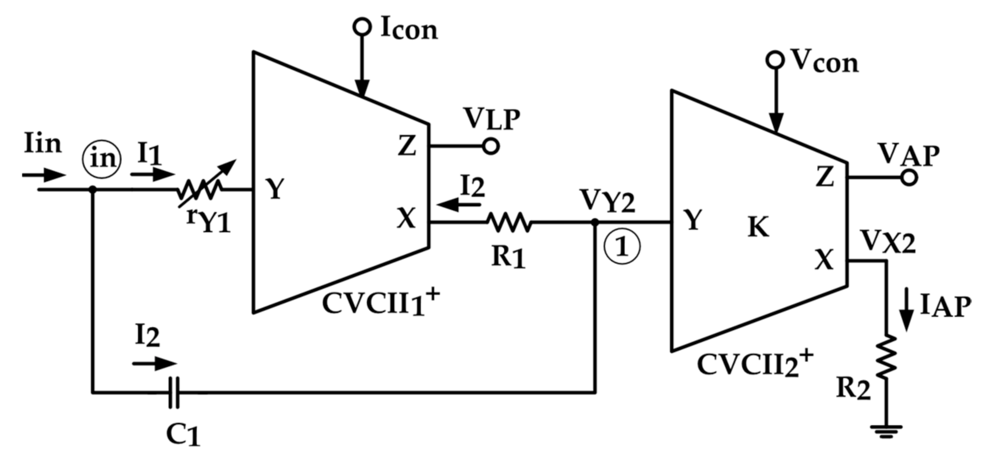
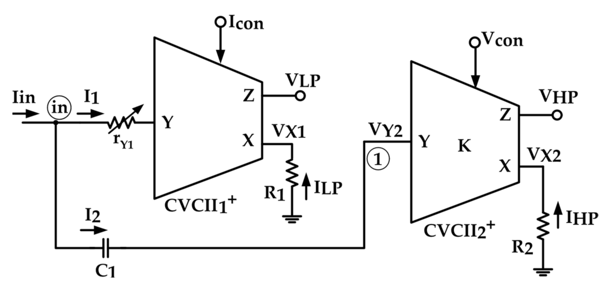
2. The Proposed Filters

Symbolic representations of CVCII with electronically tunable Y port impedance and electronically tunable current gain at X terminal are shown in Figure 1a,b, respectively. The operation matrix of CVCII with electronically variable impedance at Y port is given in (1a). Here, the current gain between the Y and X ports and the voltage gain between X and Z ports are ±1 (+1 for CVCII+ and −1 for CVCII−). The impedance at Y port is shown by r Y which can be tuned by I con . The operation of CVCII with electronically variable current gain is given in (1b). In this case, the impedance value at the Y port is ideally zero, the value of the voltage gain between the X and Z ports is unity, while the value of current gain between Y and X ports is ±K (+K for CVCII+ and −K for CVCII−) which is adjusted by the control voltage V con .
I X V Z V Y = ± 1                 0               0 0                   1             0 r Y               0               0 I Y V X I Z
I X V Z V Y = ± K                 0               0 0                   1             0 0                   0               0 I Y V X I Z
The proposed LP/AP filter topology is shown in Figure 2. It is based on one CVCII1+ with electronically variable impedance at Y port and one CVCII2+ with electronically variable current gain, one capacitor C 1 and two external resistors R1 and R2. The input signal is in current form and the produced outputs are V LP , I AP and V AP . The voltages V LP and V AP are available at the low impedance Z ports, while the current I AP is available at the high impedance X port.
By assuming Y port of CVCII2+ at ground (since in ideal case r Y 2 = 0 ), and performing the Kirchhoff current law (KCL) at input port (named as “in”) results:
I 1 = 1 1 + sC 1 r Y 1 I in
I 2 = sC 1 r Y 1 1 + sC 1 r Y 1 I in
Using (1) and (2), V LP = V X 1 is found as:
V LP = V X 1 = R 1 1 + sC 1 r Y 1 I in
Performing KCL at node 1 and using (1) and (3) result:
I AP = K 1 sC 1 r Y 1 1 + sC 1 r Y 1 I in
V AP = KR 2 ( 1 sC 1 r Y 1 1 + sC 1 r Y 1 ) I in
As is seen from Equations (5) and (6), the AP pole frequency is expressed by (7a) which is electronically controlled by r Y 1 , while the low frequency gain of I AP and V AP are expressed in (7b) and (7c), respectively:
f 0 = 1 2 π C 1 r Y 1
Gain I AP = K
Gain V AP = KR 2
From Equation (7b,c), we can say that the gain is also electronically controllable by K .
The proposed LP/HP filter topology is shown in Figure 3. In this topology the outputs are V LP , I LP , V HP and I HP . Repeating the same analysis gives Equation (4) for V LP while I LP is found as in the previous topology:
I AP = K 1 sC 1 r Y 1 1 + sC 1 r Y 1 I in
The HP current and voltage outputs are found as:
I HP = K sC 1 r Y 1 1 + sC 1 r Y 1 I in
V HP = KR 2 sC 1 r Y 1 1 + sC 1 r Y 1 I in
From Equations (9) and (10) it is seen that both of the gain and center frequency are electronically controllable while in the LP output only f 0 is electronically controllable. Fortunately, the voltage and current outputs are available at low impedance Z ports and high impedance X ports of the used CVCIIs, respectively. It must be mentioned that although outputs in both the forms of current and voltage signals are produced, current and voltage signals of the same type are not simultaneously available. This can be considered as the main limitation of the proposed circuit. It also employs a floating capacitor, which is not desirable from the integration point of view.

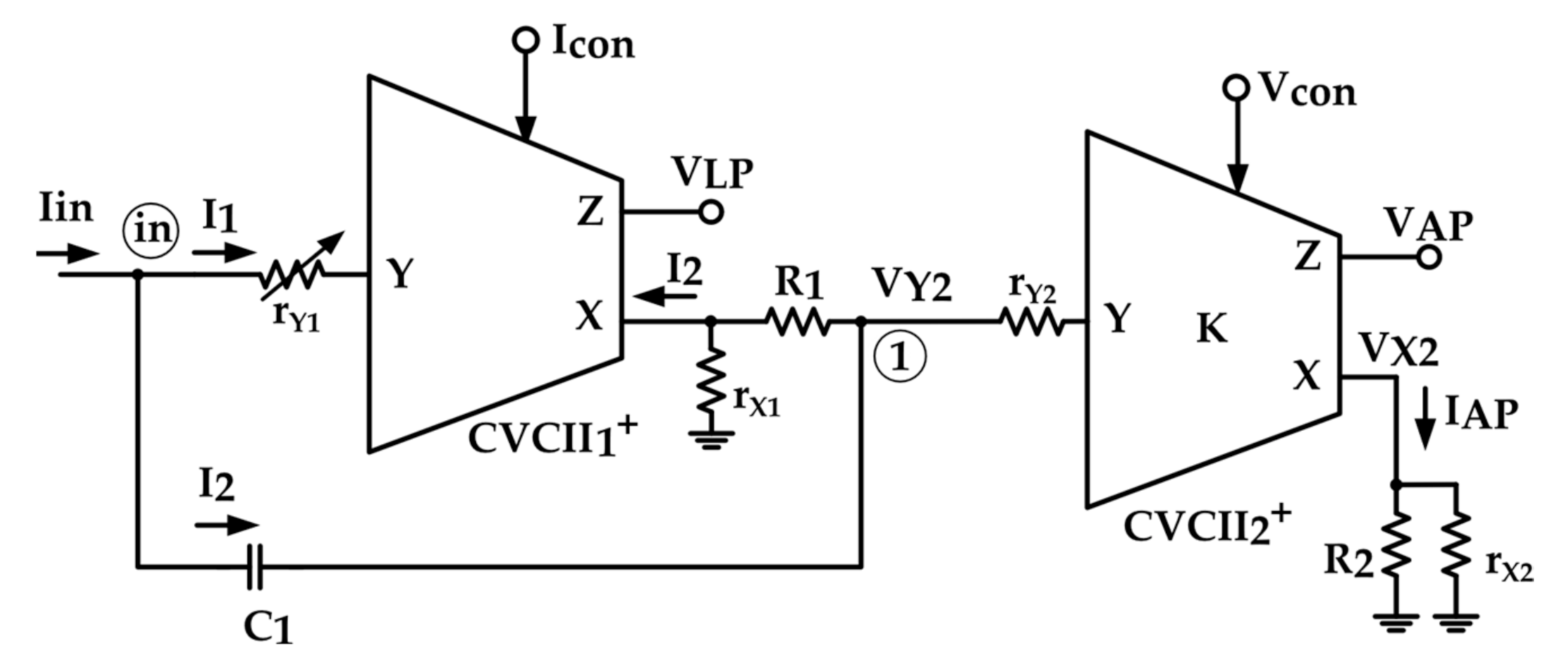
3. Nonideal Analysis

The matrix operation of the used CVCII+s in a nonideal condition is shown in (11). Here, current gain between Y and X ports for CVCII1+ is shown by β , which has a close to unity value and it is shown by K for CVCII2+, which is controllable by V con . The nonideal voltage gain between the X and Z ports for CVCII1+ and CVCII2+ is shown by α with a value close to unity. The parameters r x and r z are the parasitic impedances at the X and Z ports. In CVCII1+ r y is the parasitic impedance at Y port which is controllable by I con . For CVCII2+ r y is a nonzero constant value in the range of a few Ω.
I X V Z V Y = β K         1 / r x           0 0                       α             r z r Y                     0                     0 I Y V X I Z
Figure 4 shows the proposed LP/AP filter of Figure 2 in nonideal condition where all parasitic elements are modeled. The parasitic elements related to the CVCII1+ are named r Y 1 and r X 1 while those related to the CVCII2+ are named r Y 2 and r X 2 .
By assuming r Y 2 R 1 and r Y 2 r X 1 , we have:
I 1 = 1 + sC 1 r Y 2 1 + sC 1 r Y 1 + r Y 2 I in
I 2 = sC 1 r Y 1 1 + sC 1 r Y 1 + r Y 2 I in
Using (11)–(13) and assuming sC 1 r Y 2 1 , V x 1 and V LP are found, respectively, as:
V X 1 β 1 R 1 1 1 + sC 1 r Y 1 + r Y 2 I in
V LP β 1 α 1 R 1 1 1 + sC 1 r Y 1 + r Y 2 I in
where α 1 and β 1 are related to CVCII1+.
Performing KCL at node 1 and using (14) and (15) results in:
I AP β 1 K 1 sC 1 r Y 1 β 1 r Y 2 1 + sC 1 r Y 1 + r Y 2 I in
V AP β 1 K α 2 ( R 2 / / r X 2 ) 1 sC 1 r Y 1 β 1 r Y 2 1 + sC 1 r Y 1 + r Y 2 I in
where K and α 2 are current gain and voltage gains related to CVCII2+, respectively. The corresponding phase for the AP outputs is:
φ ω = 180 ° arctan ω C 1 r Y 1 β 1 r Y 2 arctan ω C 1 r Y 1 + r Y 2
From (18), it is noted that to reduce the effect of parasitic and nonideal elements on AP response, we must have r Y 1 r Y 2 . This condition is easily met because r Y 1 and r Y 2 are in the range of a few kΩ and a few tens of Ω, respectively. The value of β 1 is also close to unity.
Performing similar nonideal analysis for the LP/HP filter of Figure 3 results:
I LP = β 1 1 + sC 1 r Y 2 1 + sC 1 r Y 1 + r Y 2 I in
V LP = β 1 R 1 α 1 1 + sC 1 r Y 2 1 + sC 1 r Y 1 + r Y 2 I in
I HP = K sC 1 r Y 1 1 + sC 1 r Y 1 + r Y 2 I in
V HP = K ( R 2 / / r X 2 ) α 2 sC 1 r Y 1 1 + sC 1 r Y 1 + r Y 2 I in

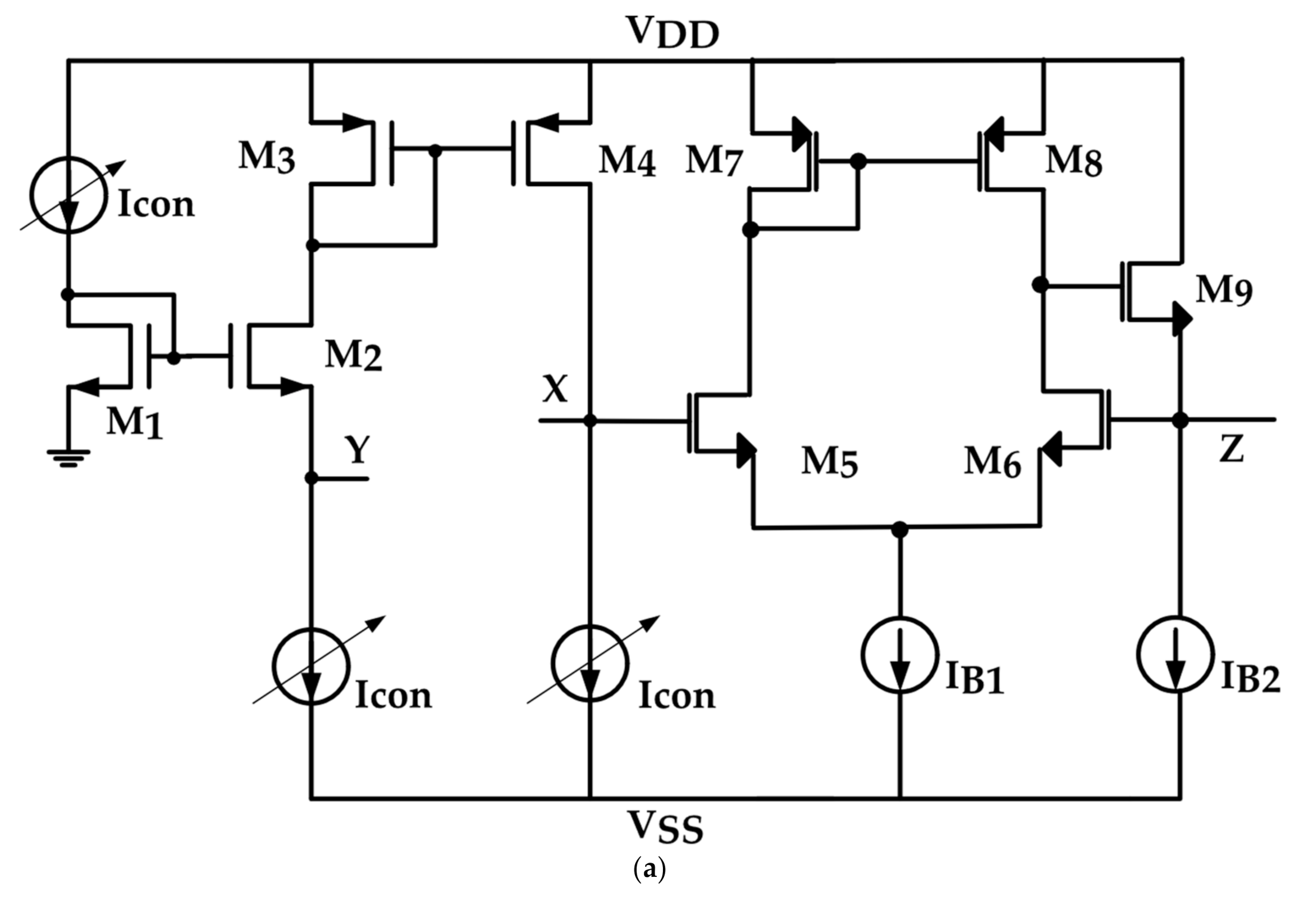
4. Internal Implementation of the Used CVCIIs

A possible CMOS implementation of the used CVCII1+ is shown in Figure 5a. Although here the current sources are shown as ideal for simplicity, in simulations they are implemented by simple current mirrors. The input section at the Y port is composed of the common gate transistor M 2 . The current sources I B 1 and I B 2 are used for biasing purposes, while I con is a variable current source which is used to set the value of impedance at the Y port. The diode connected transistor M 1 provides proper bias voltage at M 1 gate. The impedance at Y port can be expressed as:
r Y 1 = 1 gm M 2
where gm M 2 (with usual meaning of symbols) is:
gm M 2 = μ C ox W M 2 L M 2 I con
As is seen from (24), the value of gm M 2 is controllable by I con . Therefore, the appropriate value of the Y port impedance can be achieved by setting the value of I con . To set zero offset voltage at the Y port, I con is also applied to the drain of M 1 , so the DC value of gate–source voltage of M 1 and M 2 is kept equal, resulting in zero DC offset voltage at Y port.
The input current applied to the Y terminal is transferred to the X terminal through a simple current mirror made of M 3 M 4 . The voltage produced at the X port is transferred to the Z port through voltage buffer made of M 5 M 9 transistors. Here, the low impedance at the Z port is provided by negative feedback loop realized by M 9 . The CVCII2+ shown in Figure 5b is formed by a series connection of a current buffer made of M 1 M 7 , M 6 C M 7 C transistors and a voltage buffer formed by M 8 M 12 transistors. The required low impedance at the Y terminal is provided by negative feedback loop established with M 5 . By connecting the gate of M 1 at the ground, the DC value of the Y port offset voltage is set at ground. The used degenerated current mirror, made of M 6 , M 6 C , M 7 , M 7 C transistors, transfers the input current from Y to X terminals. As it was previously used in [39,40], by setting the value of V con , the gain of the current mirror is tuned resulting in a variable current gain between Y and X ports. The current gain between X and Y terminals ( K ) is expressed by (25) with usual meaning of symbols.
K = gm M 6 gm M 7 1 + gm M 6 rds M 6 C 1 + gm M 7 rds M 7 C
Similar to CVCII1+ of Figure 5a, in the voltage buffer section, the voltage produced at the X terminal is transferred to the Z terminal through voltage buffer formed by the M 8 M 12 transistors. The negative feedback loop made of M 12 provides low impedance at the Z port.
being:
rds M 7 c = 1 µ C ox W M 7 C L M 7 C V dd V con V THP
rds M 6 c = 1 µ C ox W M 6 C L M 6 C V dd V THP

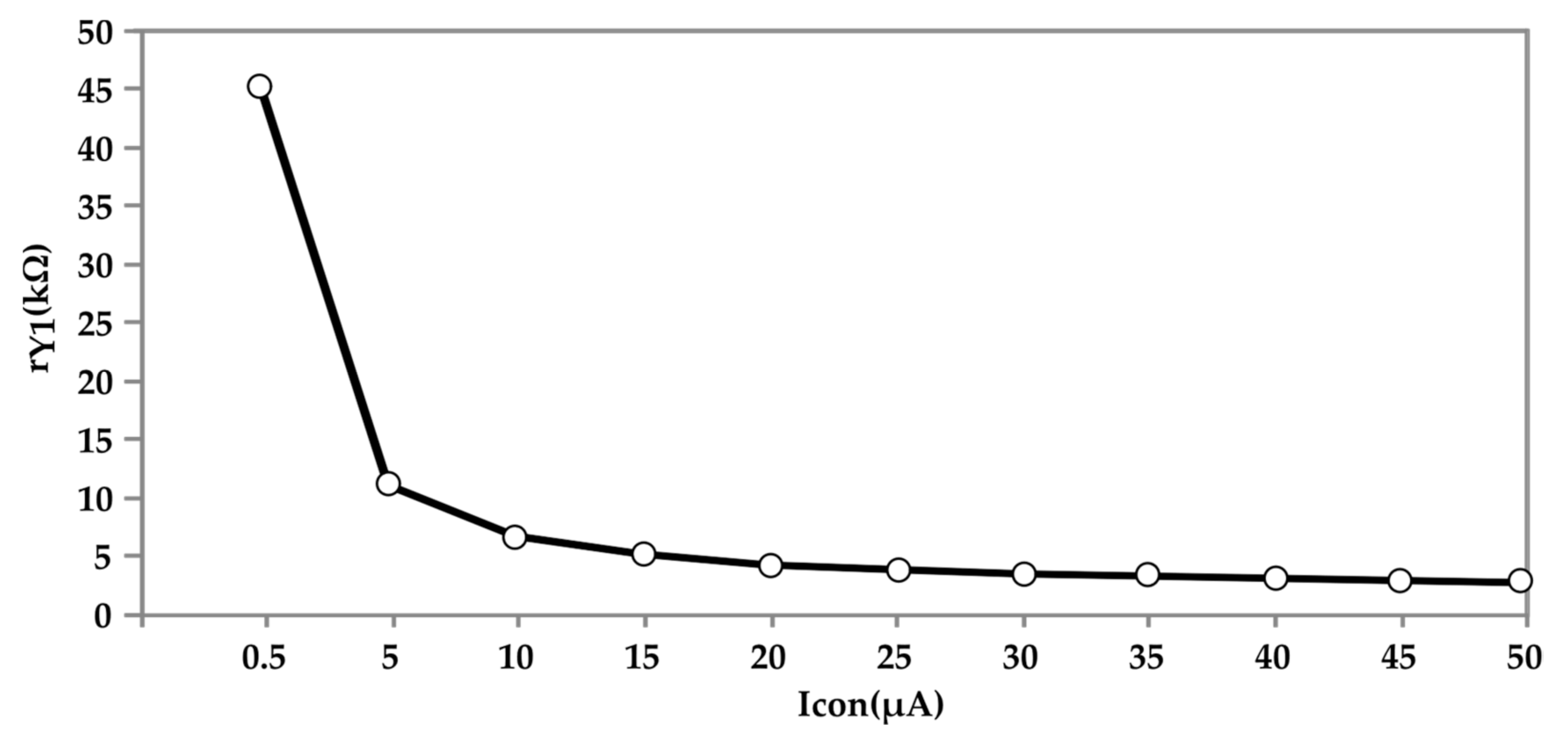
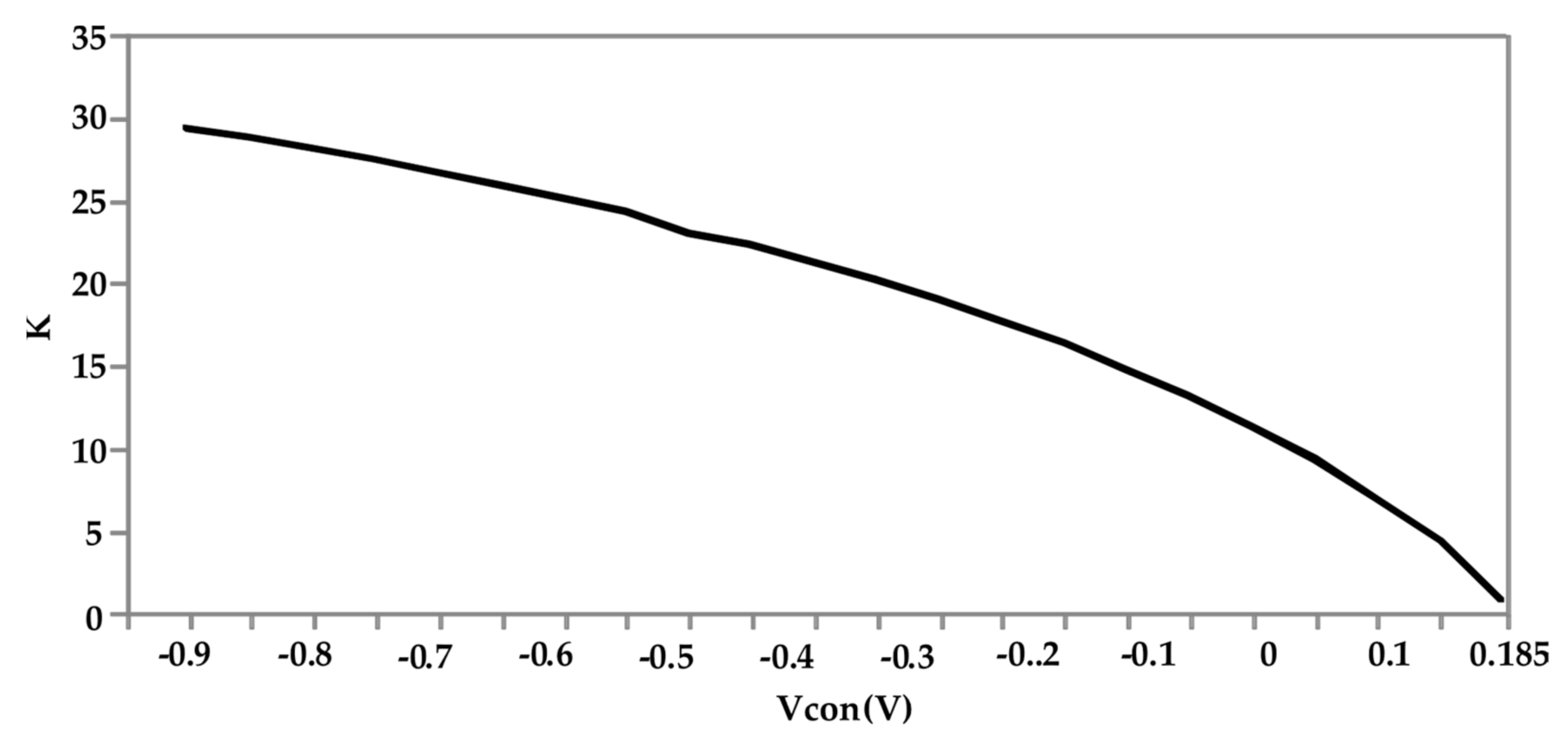
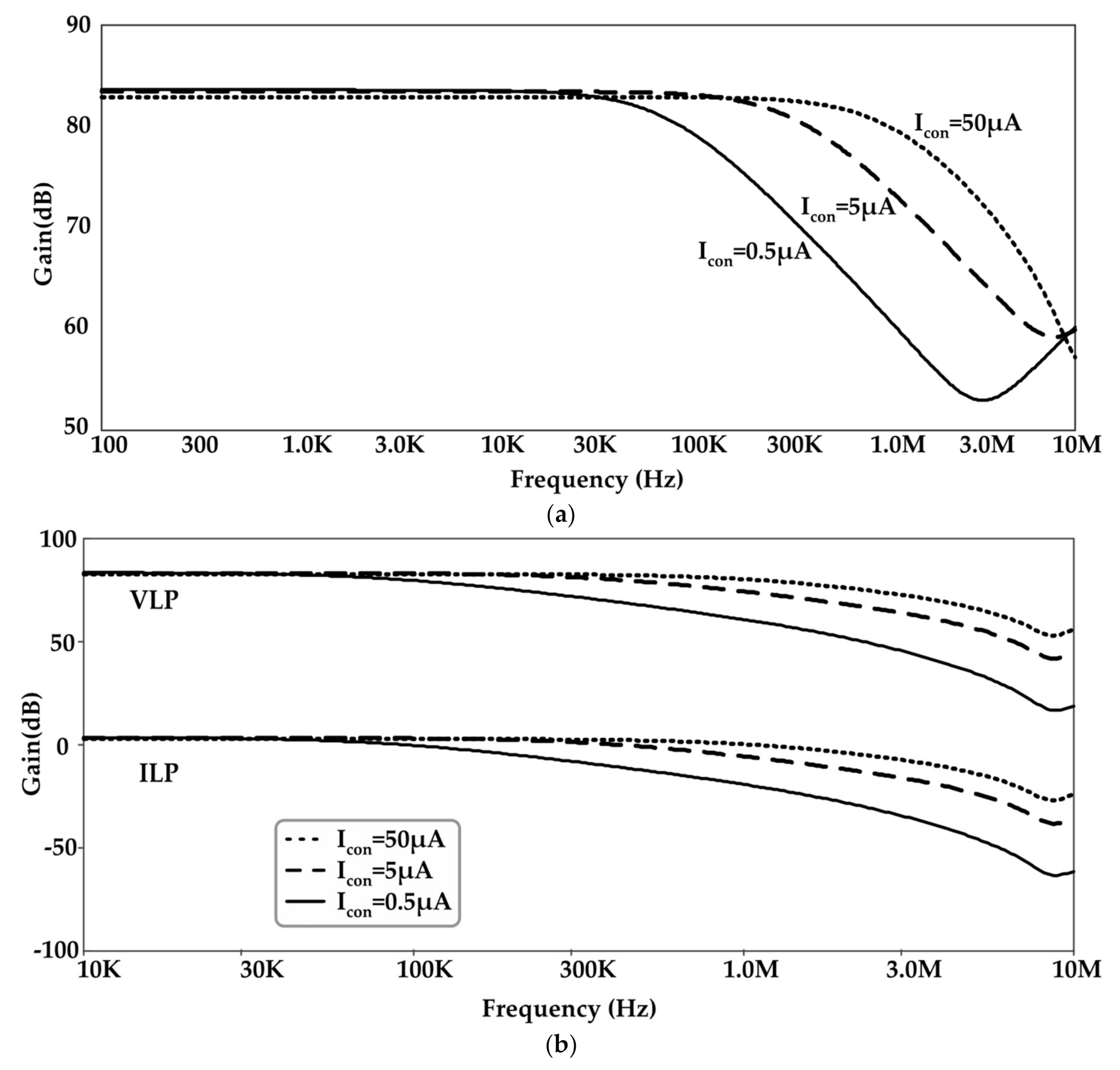
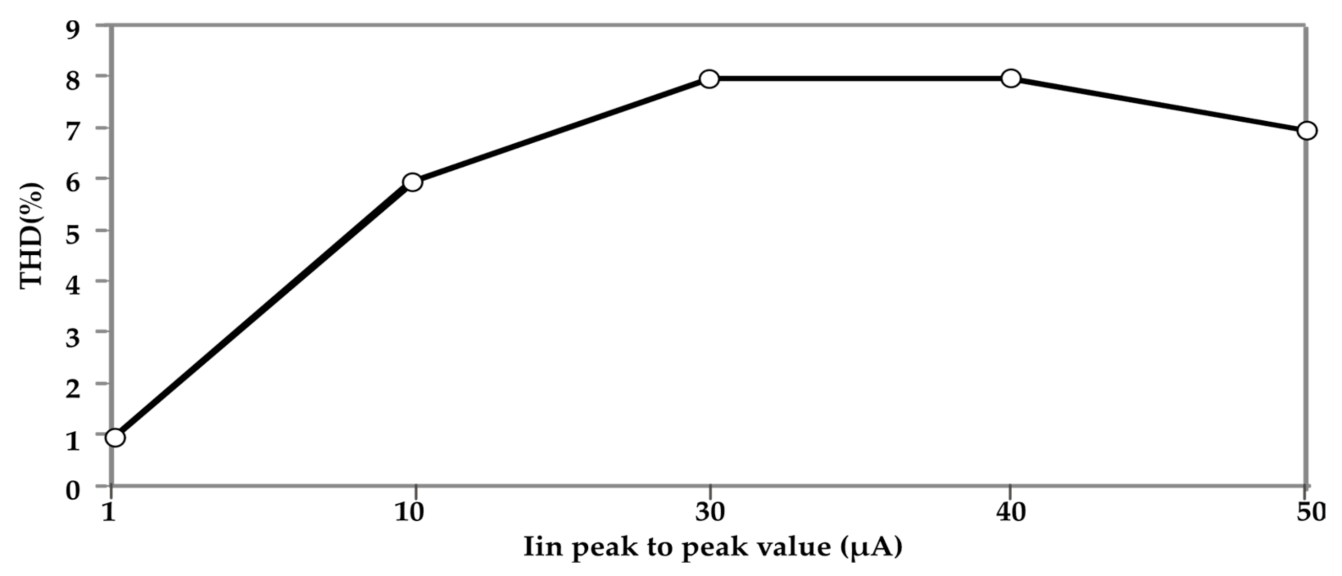
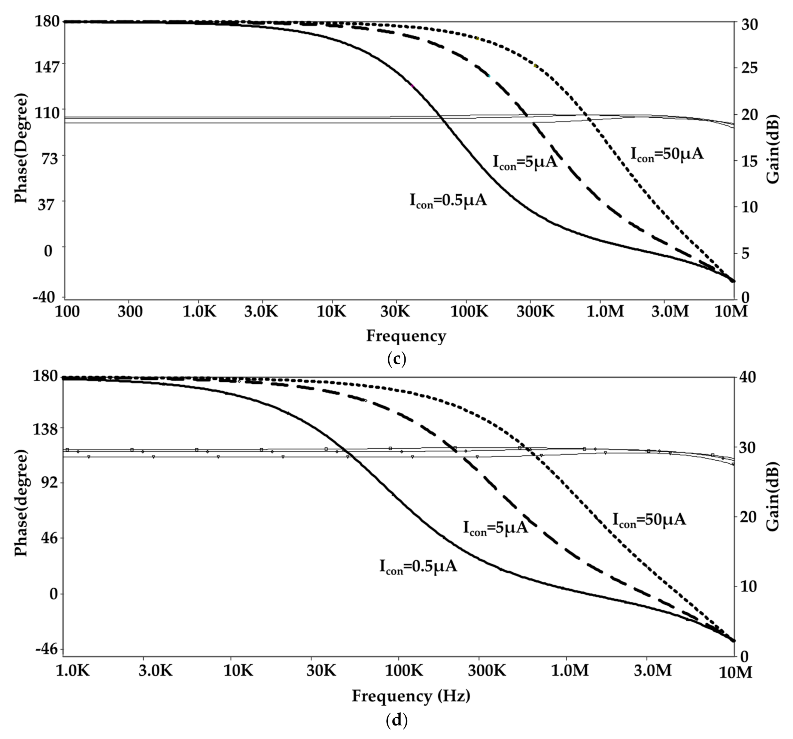
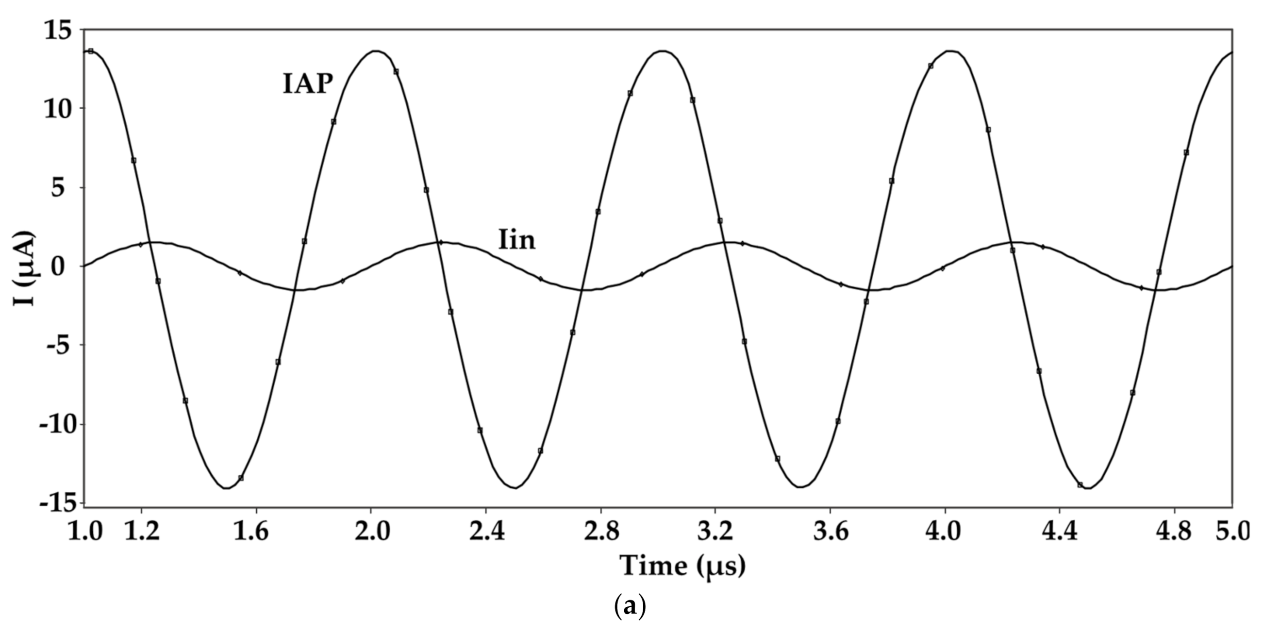
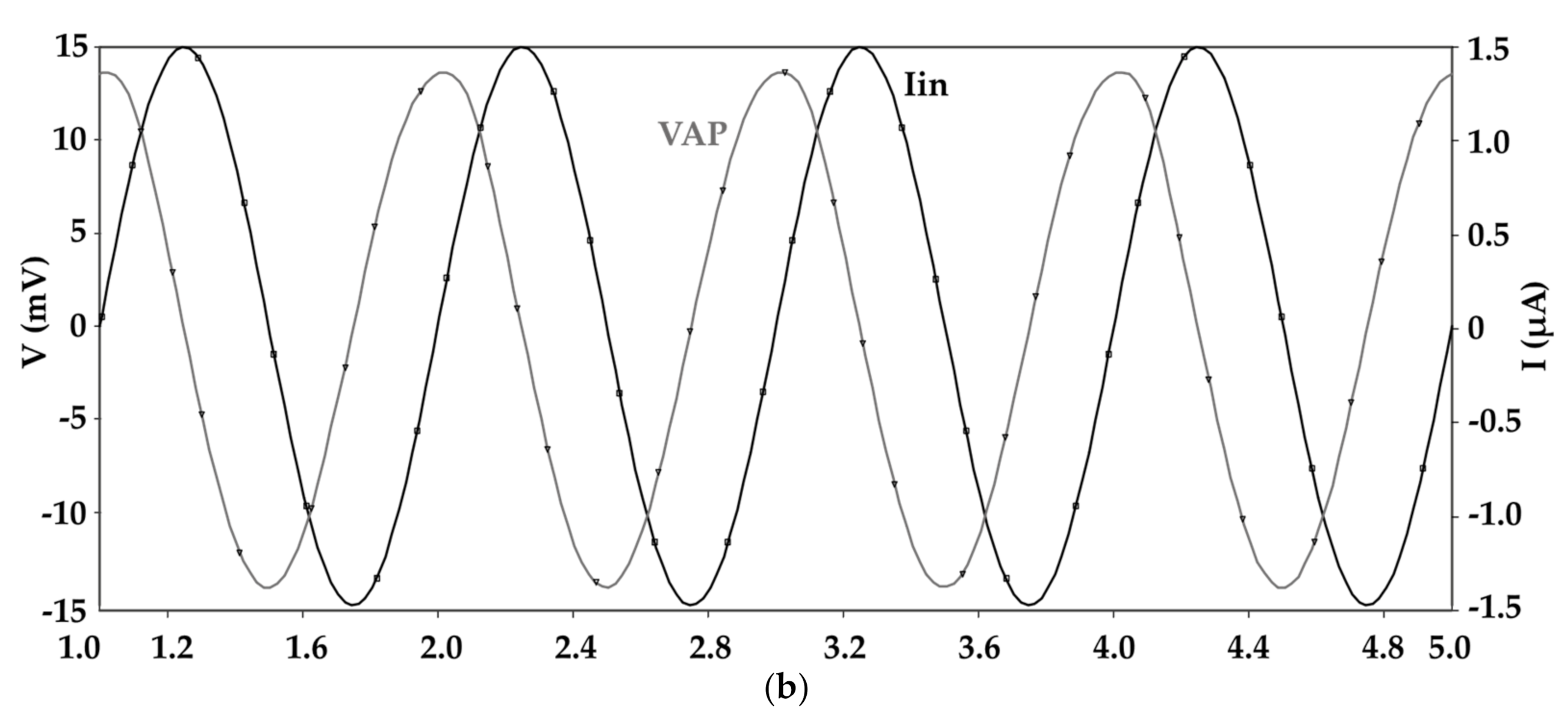
5. Simulation Results

The proposed electronically tunable LP/AP filter of Figure 2 and LP/HP filter of Figure 3 has been simulated using SPICE and 0.18 μm CMOS technology parameters and supply voltage of ±0.9 V. The used transistors aspect ratios are reported in Table 1. The values of the bias current sources which are realized by simple current mirrors are reported in Table 2. The performance parameters of CVCII1+ and CVCII2+ are summarized in Table 3. The variation of CVCII1+ Y port impedance ( r Y 1 ) by I con is shown in Figure 6. As is seen, by increasing I con from 0.5 µA to 50 µA the value of r Y 1 varies from 45 kΩ to 3.5 kΩ. The variation of CVCII1+ power consumption is from 0.101 mW to 0.423 mW for I con = 0.5 µA and I con = 50 µA, respectively. The variation of CVCII2+ current gain K versus V con is shown in Figure 7. As is seen, K falls from 30 to 1 while V con varies from −0.9 V to 0.185 V. The variation of CVCII2+ power consumption is 0.284 mW and 0.634 mW for V con = 0.185 V and V con = −0.9 V, respectively.
In the filters presented in Figure 2 and Figure 3 we have set the values of C 1 , R 1 and R 1 as 20 pF, 15 kΩ and 1 kΩ, respectively. The frequency performance of LP output for three different values of I con is shown in Figure 8. It is seen that the −3 dB frequency is 89 kHz, 370 kHz and 1 MHz for I con = 0.5 µA, I con = 5 µA and I con = 50 µA, respectively. The low frequency gain value is about 83 dB. To test the time domain response of LP output, a sinusoidal input signal with peak to peak value of 10 µA and frequency of 1 MHz is used as input signal with I con = 50 µA. The resulted total harmonic distortion (THD) is shown in Figure 9, which shows maximum value of 8% for THD at LP output.
Figure 10 shows the gain and phase frequency performances of the I AP and V AP outputs for different values of I con and V con from which the electronic tunability of both frequency and gain is evident. To examine the time domain performance of the proposed AP filter, a sinusoidal input with peak-to-peak amplitude of 2 μA and frequency of 1 MHz is applied to the proposed circuit. For I con = 50 µA and V con = 0 V, the input and output signals are shown in Figure 11, where an 87° phase shift for both produced I AP and V AP is found. In this case, THD is 2%.
Figure 12 reports the frequency performances of I HP and V HP outputs for different values of I con and V con . The value of f 0 for HP outputs is 81 kHz, 360 kHz and 1 MHz for I con = 0.5 µA, 5 µA and 50 µA, respectively. The gain of I HP varies from 0.980 dB to 29 dB for V con variation from 0.185 V to −0.9 V. For V HP gain, variation is from 60 dB to 88.9 dB. The THD values are 7.7% and 10% for I HP and V HP for input signal of 1 MHz and 5 µA peak to peak value and I con = 50 µA and V con = −0.9 V.
A comparison between the proposed circuit and other previously reported ones is given in Table 3. As is seen, the proposed circuit offers many advantages, such as full electronic controllability, being free from any matching condition, versatility for providing both current and voltage signals, providing both LP and AP outputs and simple implementation compared to the available works. However, the proposed circuit employs a floating capacitor, which is not desirable from an integration point of view.

6. Conclusions

Two new electronically tunable first order LP/AP and LP/HP filter topologies based on two CVCIIs, two resistors and one capacitor have been presented. The first topology produces V LP / I AP / V AP outputs and second topology produces I LP / V LP / I HP / V HP outputs. The f 0 of LP output is electronically tunable while both f 0 and gain of AP and HP outputs are fully electronically tunable using electronically variable VCII. The value of f 0 is controlled by I con , which is used to vary the Y port impedance of the first CVCII. The gains are also controlled by V con , which is used to change the current gain of the second CVCII. The circuit is free from any matching condition. The total number of used transistors is only 36. Due to the circuit’s simplicity, the proposed circuit enjoys high frequency performance compared to its counterparts. The only drawback of the proposed circuit is that it employs a floating capacitor.

Author Contributions

Conceptualization, L.S. and G.B.; methodology, L.S., G.F.; validation, G.F., V.S. and L.P.; formal analysis, L.S.; investigation, V.S.; data curation, L.S. and G.B.; writing—original draft preparation, L.S.; writing—review and editing, G.F., G.B.,V.S. and L.P.; supervision, G.F. All authors have read and agreed to the published version of the manuscript.

Funding

This research received no external funding.

Conflicts of Interest

The authors declare no conflict of interest.

References

  1. Minaei, S.; Yuce, E. Unity/Variable-Gain Voltage-Mode/Current-Mode First-Order All-Pass Filters Using Single Dual-X Second-Generation Current Conveyor. IETE J. Res. 2010, 56, 305–312. [Google Scholar] [CrossRef] [Green Version]
  2. Kaçar, F.; Özcelep, Y. CDBA Based Voltage-Mode First-Order All-Pass Filter Topologies. Istanb. Univ. J. Electric. Electron. Eng. 2011, 11, 1327–1332. [Google Scholar]
  3. Metin, B.; Pal, K.; Cicekoglu, O. CMOS-Controlled Inverting CDBA with a New All-Pass Filter Application. Int. J. Circuit Theory Appl. 2011, 39, 417–425. [Google Scholar] [CrossRef]
  4. Ibrahim, M.; Minaei, S.; Yuce, E. All-Pass Sections with High Gain Opportunity. Radio Eng. 2011, 20, 3–9. [Google Scholar]
  5. Das, R.; Paul, S.K. Voltage Mode First Order All Pass Filter Design Using Differential Difference Current Conveyor. In Proceedings of the 2016 International Conference on Microelectronics, Computing and Communications (MicroCom), Durgapur, India, 23–25 January 2016; pp. 1–4. [Google Scholar]
  6. Dixit, V.K.; Gupta, R.; Pal, K. High-Input Impedance First Order All-Pass Filters Using DDCC. In Proceedings of the 2013 Annual IEEE India Conference (INDICON), Mumbai, India, 13–15 December 2013; pp. 1–5. [Google Scholar]
  7. Toker, A.; Özcan, S.; Kuntman, H. Supplementary All-Pass Sections with Reduced Number of Passive Elements Using a Single Current Conveyor. Int. J. Electron. 2001, 88, 969–976. [Google Scholar] [CrossRef]
  8. Pal, K.; Rana, S. Some New First-Order All-Pass Realizations Using CCII. Act. Passive Electron. Compon. 2004, 27, 91–94. [Google Scholar] [CrossRef] [Green Version]
  9. Metin, B.; Cicekoglu, O. Novel First Order All-Pass Filter with a Single CCI. In Proceedings of the MELECON 2006—2006 IEEE Mediterranean Electrotechnical Conference, Malaga, Spain, 16–19 May 2006; Institute of Electrical and Electronics Engineers (IEEE); pp. 74–75. [Google Scholar]
  10. Beg, P.; Ansari, M.S. Fully-differential first-order all-pass filters using CMOS DV-DXCCII. In Proceedings of the 2017 International Conference on Multimedia, Signal Processing and Communication Technologies (IMPACT), Aligarh, India, 24–26 November 2017; Institute of Electrical and Electronics Engineers (IEEE); pp. 267–270. [Google Scholar]
  11. Horng, J.-W.; Hou, C.-L.; Chang, C.-M.; Chung, W.-Y.; Liu, H.-L.; Lin, C.-T. High output impedance current-mode first-order allpass networks with four grounded components and two CCIIs. Int. J. Electron. 2006, 93, 613–621. [Google Scholar] [CrossRef]
  12. Herencsar, N.; Lahiri, A.; Koton, J.; Vrba, K. First-order multifunction filter design using current amplifiers. In Proceedings of the 2016 39th International Conference on Telecommunications and Signal Processing (TSP), Vienna, Austria, 27–29 June 2016; Institute of Electrical and Electronics Engineers (IEEE); pp. 279–282. [Google Scholar]
  13. Kilinç, S.; Cam, U.; Kılınç, S. Current-Mode First-Order Allpass Filter Employing Single Current Operational Amplifier. Analog. Integr. Circuits Signal Process. 2004, 41, 47–53. [Google Scholar] [CrossRef]
  14. Ibrahim, M.A.; Kuntman, H.; Ozcan, S.; Suvak, O.; Cicekoglu, O. New first-order inverting-type second-generation current conveyor-based all-pass sections including canonical forms. Electr. Eng. 2003, 86, 299–301. [Google Scholar] [CrossRef]
  15. Maheshwari, S.; Khan, I.A. Novel first order all-pass sections using a single CCIII. Int. J. Electron. 2001, 88, 773–778. [Google Scholar] [CrossRef]
  16. Kacar, F. Operational Transresistance Amplifier Based Current-Mode All-Pass Filter Topologies. In Proceedings of the 2009 Applied Electronics, Pilsen, Czech Republic, 9–10 September 2009; pp. 149–152. [Google Scholar]
  17. Kumar, A.; Paul, S.K. Current mode first order universal filter and multiphase sinusoidal oscillator. AEU Int. J. Electron. Commun. 2017, 81, 37–49. [Google Scholar] [CrossRef]
  18. Nand, D.; Pandey, N. Transadmittance Mode First Order LP/HP/AP Filter and its Application as an Oscillator. IOP Conf. Series: Mater. Sci. Eng. 2017, 225, 012150. [Google Scholar] [CrossRef]
  19. Chaturvedi, B.; Mohan, J.; Jitender; Kumar, A. A Novel Realization of Current-Mode First Order Universal Filter. In Proceedings of the 2019 6th International Conference on Signal Processing and Integrated Networks (SPIN), Noida, India, 7–8 March 2019; Institute of Electrical and Electronics Engineers (IEEE); pp. 623–627. [Google Scholar]
  20. Fabre, A.; Saaid, O.; Wiest, F.; Boucheron, C. High frequency applications based on a new current controlled conveyor. IEEE Trans. Circuits Syst. I Regul. Pap. 1996, 43, 82–91. [Google Scholar] [CrossRef]
  21. Safari, L.; Minaei, S.; Yuce, E. CMOS First-Order Current-Mode All-Pass Filter with Electronic Tuning Capability and Its Applications. J. Circuits Syst. Comput. 2013, 22, 1350007. [Google Scholar] [CrossRef]
  22. Safari, L.; Yuce, E.; Minaei, S. A new ICCII based resistor-less current-mode first-order universal filter with electronic tuning capability. Microelectron. J. 2017, 67, 101–110. [Google Scholar] [CrossRef]
  23. Tangsrirat, W. On the Realization of First-Order Current-Mode AP/HP Filter. Radioengineering 2013, 22, 1007–1015. [Google Scholar]
  24. Maheshwari, S. A new current-mode current-controlled all-pass section. J. Circuits Syst. Comput. 2007, 16, 181–189. [Google Scholar] [CrossRef]
  25. Tangsrirat, W.; Pukkalanun, T.; Surakampontorn, W. Resistorless realization of current-mode first-order allpass filter using current differencing transconductance amplifiers. Microelectron. J. 2010, 41, 178–183. [Google Scholar] [CrossRef]
  26. Noppakarn, A.; Lawanwisut, S. New Gain Controllable Resistor-Less Current-Mode First Order Allpass Filter and Its Application. Radioengineering 2011, 21, 312–316. [Google Scholar]
  27. Maheshwari, S. Grounded capacitor cm-aps with high output impedance. J. Circuits Syst. Comput. 2007, 16, 567–576. [Google Scholar] [CrossRef]
  28. Maheshwari, S. New voltage and current-mode APS using current controlled conveyor. Int. J. Electron. 2004, 91, 735–743. [Google Scholar] [CrossRef]
  29. Öztayfun, S.; Kılınç, S.; Çelebi, A.; Çam, U. A new electronically tunable phase shifter employing current-controlled current conveyors. AEU Int. J. Electron. Commun. 2008, 62, 228–231. [Google Scholar] [CrossRef]
  30. Kumngern, M.; Chanwutitum, J. An Electronically Tunable Current-Mode First-Order Allpass Filter Using a CCCCTA. In Proceedings of the 2013 International Conference on Advanced Technologies for Communications (ATC 2013), Ho Chi Minh City, Vietnam, 16–18 October 2013; pp. 733–736. [Google Scholar]
  31. Chaichana, A.; Kumngern, M.; Siripruchyanun, M.; Jaikla, W. Amplitude Controllable Current-Mode First Order Allpass Filter Including Minimum Component Count Circuits. In Proceedings of the 2015 38th International Conference on Telecommunications and Signal Processing (TSP), Prague, Czech Republic, 9–11 July 2015; pp. 1–4. [Google Scholar]
  32. Herencsar, N.; Jerabek, J.; Koton, J.; Vrba, K.; Minaei, S.; Cem Goknar, I. Pole Frequency and Pass-Band Gain Tunable Novel Fully-Differential Current-Mode All-Pass Filter. In Proceedings of the 2015 IEEE International Symposium on Circuits and Systems (ISCAS), Lisbon, Portugal, 24–27 May 2015. [Google Scholar]
  33. Safari, L.; Barile, G.; Stornelli, V.; Ferri, G. An Overview on the Second Generation Voltage Conveyor: Features, Design and Applications. IEEE Trans. Circuits Syst. II Express Briefs 2018, 66, 547–551. [Google Scholar] [CrossRef]
  34. Safari, L.; Barile, G.; Ferri, G.; Stornelli, V. A New Low-Voltage Low-Power Dual-Mode VCII-Based SIMO Universal Filter. Electronics 2019, 8, 765. [Google Scholar] [CrossRef] [Green Version]
  35. Barile, G.; Ferri, G.; Safari, L.; Stornelli, V. A New High Drive Class-AB FVF-Based Second Generation Voltage Conveyor. IEEE Trans. Circuits Syst. II Express Briefs 2019, 67, 405–409. [Google Scholar] [CrossRef]
  36. Safari, L.; Barile, G.; Stornelli, V.; Ferri, G.; Leoni, A. New Current Mode Wheatstone Bridge Topologies with Intrinsic Linearity. In Proceedings of the PRIME 2018—14th Conference on Ph.D. Research in Microelectronics and Electronics, Prague, Czech Republic, 2–5 July 2018. [Google Scholar]
  37. Safari, L.; Barile, G.; Ferri, G.; Stornelli, V. High performance voltage output filter realizations using second generation voltage conveyor. Int. J. RF Microw. Comput. Eng. 2018, 28, 21534. [Google Scholar] [CrossRef]
  38. Yuce, E.; Safari, L.; Minaei, S.; Ferri, G.; Stornelli, V. New mixed-mode second-generation voltage conveyor based first-order all-pass filter. IET Circuits Devices Syst. 2020, 14, 901–907. [Google Scholar] [CrossRef]
  39. Safari, L.; Minaei, S. A Novel Resistor-Free Electronically Adjustable Current-Mode Instrumentation Amplifier. Circuits Syst. Signal Process. 2012, 32, 1025–1038. [Google Scholar] [CrossRef]
  40. Safari, L.; Minaei, S. New ECCII-Based Electronically Controllable Current-Mode Instrumentation Amplifier with High Frequency Performance. In Proceedings of the 2017 European Conference on Circuit Theory and Design (ECCTD), Catania, Italy, 4–6 September 2017; pp. 1–4. [Google Scholar]
Figure 1. Symbolic representation of second generation voltage conveyor (CVCII+) with (a) variable impedance at Y port and (b) variable current gain.
Electronics 10 00822 g001
Figure 2. The proposed CVCII based low-pass/all-pass (LP/AP) filter topology.
Electronics 10 00822 g002
Figure 3. The proposed LP/HP filter topology.
Electronics 10 00822 g003
Figure 4. The proposed LP/AP filter topology (shown in Figure 2) in nonideal condition.
Electronics 10 00822 g004
Figure 5. CMOS implementation of the used (a) CVCII1+ and (b) CVCII2+.
Electronics 10 00822 g005aElectronics 10 00822 g005b
Figure 6. Variation of r Y 1 as a function of I con for CVCII1+.
Electronics 10 00822 g006
Figure 7. Variation of K as a function of V con for CVCII2+.
Electronics 10 00822 g007
Figure 8. Frequency performance of LP output for different values of I con for the filters represented in Figure 2a and Figure 3b.
Electronics 10 00822 g008
Figure 9. Low-pass (LP) output total harmonic distortion (THD) value for a sinusoidal input signal with frequency of 1 MHz ( I con = 50 µA) at different values of input signal for the filter reported in Figure 2.
Electronics 10 00822 g009
Figure 10. Gain and phase frequency response of (a) V AP for V con = 0 V, (b) V AP for V con = −0.9 V, (c) I AP for V con = 0 and (d) I AP for V con = −0.9 V.
Electronics 10 00822 g010aElectronics 10 00822 g010b
Figure 11. Time domain outputs for (a) I AP and (b) V AP in the case of I con = 50 µA and V con = 0 V.
Electronics 10 00822 g011aElectronics 10 00822 g011b
Figure 12. Gain frequency response of (a) I HP for V con = 0.185 V (b) I HP for V con = −0.9 V (c) V HP for V con = 0.185 V and (d) V HP for V con = −0.9 V at three different values of I con for the filter proposed in Figure 3.
Electronics 10 00822 g012aElectronics 10 00822 g012b
Table 1. CVCII1+ and CVCII2+ main transistors aspect ratio and bias currents.
W, L
CVCII1+CVCII2+
M 1 ,   M 2 4.5 µm, 4.5 µm7.2 µm, 1.8 µm
M 3 ,   M 4 90 µm, 1.8 µm9 µm, 1.8 µm
M 5 3.6 µm, 1.8 µm270 µm, 0.9 µm
M 6 3.6 µm, 1.8 µm5.04 µm, 0.54 µm
M 7 9 µm, 1.8 µm50.4 µm, 0.54 µm
M 8 9 µm, 1.8 µm7.2 µm, 1.8 µm
M 9 360 µm, 0.9 µm7.2 µm, 1.8 µm
M 12 -270 µm, 0.9 µm
M 6 c -0.9 µm, 0.54 µm
M 7 c -9 µm, 0.54 µm
M 10 ,   M 11 -9 µm, 1.8 µm
I b 1 , I b 2 30 µA,30 µA28 µA,7 µA
I b 3 , I b 4 ,   I b 5 -70 µA, 28 µA, 7 µA
Table 2. Performance parameters of the designed CVCII1+ and CVCII2+.
CVCII1+CVCII2+
R Y From   45   K Ω   ( I con = 0.5 µA) to
3.5   K Ω   ( I con = 50 µA)
81 Ω
R X From   1.6   M Ω   ( I con = 0.5 µA) to
286   K Ω   ( I con = 50 µA)
From   1   M Ω   ( V con = 0 V) to
96   k   ( V con = −0.9 V)
C Y From   117   fF   ( I con = 5 µA) to
123   fF   ( I con = 50 µA)
3.3 fF
R Z 54 Ω57 Ω
DC offset at Y11 mV2.6 mV
DC offset at Z5 mV6 mV
DC offset at X6 mV−2.4 mV
A 0.9850.989
Β 0.993   for   I con = 0.5 µA and
0.965   for   I con = 50 µA
9.5
Power 101   µ W   for   I con = 0.5 µA to
423   µ W   for   I con = 50 µW
From   284   µ W   for   V con = 0.185 V to
634   µ W   for   V con = −0.9 V
Table 3. Comparison between proposed circuit and other circuits reported in the literature.
RefABB#RFloating C#
Transistors
VDD
VSS
Pd (W)OutputMatchElectronic Tunability f 0 ( Hz )
f 0 G
[1]1DXCCII2Yes 120±1.25 V2.1 m V AP 2YesNoNo1.59 M
[2]1DDCCII1Yes/No 318±2.5 VNA 4 V AP 2NoNoNo10 M
[10]DV-DXCCII2Yes 130±1.25 VNA V AP 2YesNoNo6.133 M
[12]3CA1Yes120±5 V25.7 m I AP NoNoYes100 k
[17]1Dx-MOCCII1Yes40±1.25 VNA ± I AP / I HP / I LP NoNoNo7.962 M
[18]2OFCC2No42±1.5 VNA I HP / I LP / I AP YesNoNo159 K
[19]1DD-DXCCII3Yes30±1.2 VNA I HP / I LP / I AP YesNoNo6.43 M
[21]Current Mirror0No10±0.9 V0.266 m I AP NoYesNo3 M
[22]1ICCII0Yes44±0.75 V2.75 m I LP / I AP / I HP NoYesNo2.6 M
[23]Current Mirror0No8+1.50.169 m I AP / I HP NoYesNo159 k
[24]2CCCII0Yes35±2.5 VNA + I AP / I AP NoYesNo4.8 M
[25]2CDTA0Yes84±2 V9 m + I AP / I AP NoYesNo1 M
[26]2CCCCTA0No54±2.5 VNA I AP NoYesYes<1 M
[27]Modified CCCII0No42±2.5 VNA I AP NoYesNo1 M
[28]2CCCII0Yes38NANA I AP NoYesNo58 k
200 kHz
[29]1Do-CCCII0Yes 142±3 VNA + I AP / I AP YesYesNo1.632 M
[30]1CCCTA1Yes 125±1.5 VNA I AP NoYesYes1.66 M
[31]1CFCTA1No35±1.25 V5.5 m ± I LP NoYesYes2 M
[32]1CA+2CB0Yes46±1.2 V3.88 m
5.29 m
I AP NoYesYes1.41 M
[35]1VCII±+1VCII+3No34±0.9 V0.489 m V AP / I AP YesNoNo1 M
Proposed#12CVCII+2Yes36±0.9 V0.385 m
1.057 m
I AP / V AP / V LP NoYes 5Yes89 K–1 M
Proposed#22CVCII+2Yes36±0.9 V0.385 m
1.057 m
I HP / V HP / V LP / I LP NoYesYes89 K–1 M
1 Two floating compensation capacitors are used in the internal structure of the used active building blocks (ABB); 2 Additional voltage buffer is required for V AP output; 3 There are two structures one with floating C and one without; 4 Not Available; 5 Only for AP outputs.
Publisher’s Note: MDPI stays neutral with regard to jurisdictional claims in published maps and institutional affiliations.

