Article

Optimal Tuning of Fractional Order Controllers for Dual Active Bridge-Based DC Microgrid Including Voltage Stability Assessment

by
Mohamed Azab
1,2,* and
Alexandre Serrano-Fontova
3
1
Electrical Engineering Technology Department, Faculty of Engineering, Benha University, Benha 13512, Egypt
2
Electrical Engineering Technology Department, Yanbu Industrial College, Yanbu 30436, Saudi Arabia
3
Department of Electrical Engineering, Technical University of Catalunya (UPC), 08028 Barcelona, Spain
*
Author to whom correspondence should be addressed.
Electronics 2021, 10(9), 1109; https://doi.org/10.3390/electronics10091109
Submission received: 19 March 2021 / Revised: 27 April 2021 / Accepted: 1 May 2021 / Published: 8 May 2021
(This article belongs to the Special Issue Power Converters Technologies in Power Electronics)

Abstract

:
In this article, three evolutionary search algorithms: particle swarm optimization (PSO), simulated annealing (SA) and genetic algorithms (GA), have been employed to determine the optimal parameter values of the fractional-order (FO)-PI controllers implemented in the dual active bridge-based (DAB) DC microgrid. The optimum strategy to obtain the parameters of these FO-PI controllers is still a major challenge for many power systems applications. The FO-PI controllers implemented in the DAB are used to control the DC link voltage to the desired value and limit the current flowing through the converter. Accordingly, the investigated control system has six parameters to be tuned simultaneously; Kp1, Ki1, λ1 for FO-PI voltage controller and Kp2, Ki2, λ2 for FO-PI current controller. Crucially, this tuning optimization process has been developed to enhance the voltage stability of a DC microgrid. By observing the frequency-domain analysis of the closed-loop and the results of the subsequent time-domain simulations, it has been demonstrated that the evolutionary algorithms have provided optimal controller gains, which ensures the voltage stability of the DC microgrid. The main contribution of the article can be considered in the successful application of evolutionary search algorithms to tune the parameters of FO-based dual loop controllers of a DC microgrid scheme whose power conditioner is a DAB topology.

1. Introduction

The dual active bridge (DAB) converter is considered as one of the most critical emerging topologies that have been successfully used in many electrical power applications such as DC microgrids [1,2]. The DAB offers key advantages such as a minimum size of passive filter components and high-power density when compared with other bidirectional DC-DC converters [3]. Therefore, DAB converter has gained popularity during the last decade in applications such as electric vehicles (EVs), energy management systems or DC microgrids with energy storage systems (ESS) [4,5,6,7,8].
A general average model of a DAB has been proposed in [2], whereas a simple but reliable model has been proposed in [7]. In Reference [7], the DAB converter average and small-signal models have been validated through both simulations and experimental tests for the four different control modes. The DABs have also been the object of study in [9,10,11,12,13,14,15,16,17,18,19,20]. Even though several control strategies have been explored for the DAB, the most common among practitioners is the simple phase shift modulation technique [17,18] based on conventional PI controllers [20,21]. Besides, the variable structure controllers have been employed to control the DAB’s operation, as can be seen in [22].
Given the proliferation of the DC and mixed AC/DC microgrids, some research has been carried out to evaluate the capabilities of some power electronic converters for voltage stability. In this sense, the voltage droop has been one of the most commonly adopted voltage regulation solutions in these microgrids. However, some articles have proposed modified versions of this classical voltage droop, see [23,24,25]. In particular, in [23], a disturbance observer has been designed for voltage regulation. In Reference [24], a damping controller has been designed to avoid power oscillations. Reference [25] proposed an observer-based with both voltage droop and current feedforward control in a DC microgrid.
On the other hand, voltage stability has also gained scientific researchers’ attention, see [26,27,28,29]. In fact, power oscillations are a consequence of poorly damped scenarios. Thus, some of them have investigated the DC microgrids’ stability, considering the passivity-based criterion [26,27]. The power converters impedance modelling for voltage stability in DC microgrids is explored in [28]. In Reference [29], a stability preserving criterion has been designed for DC microgrids considering a floating bus. The stability assessment with controller optimization has been analyzed in [30]. Lastly, an in-depth review of the available strategies used for voltage stability in DC systems is detailed in [31].
Microgrid controllers are used for either stabilization or regulation and are commonly based on feedforward cascaded loops with PI regulators. Nonetheless, the so-called fractional-order PI controllers (FO-PI) exhibit better characteristics compared with conventional PI ones [32,33,34,35]. Therefore, in this article, the FO-PI controllers have been utilized instead of conventional PI controllers. Owing to the existence of multiple FO controller parameters to be tuned simultaneously, evolutionary search algorithms have been employed to determine those controllers’ optimum value.
As stated above, several relevant works have been carried out for the voltage stability in DC microgrids. However, even though these works have made significant contributions with successful results in the field, the implemented controller parameters have been considered a fixed input.
This paper presents an optimal strategy to tune the FO-PI controllers implemented in the DAB-based DC microgrid. The tuning process has been carried out with a multiobjective optimization problem formulated through three different evolutionary algorithms named GA, PSO and SA. The process to achieve the optimal controller parameters for voltage stability is described below.
The first step is to obtain the three sets of controller parameters for each algorithm. For that purpose, the whole closed-loop transfer function is implemented in Matlab/Simulink, where the small-signal stability model of the DAB is considered. After that, each evolutionary algorithm is executed. Once the convergence has been achieved in the optimization processes, each algorithm’s best controller parameters are obtained.
Secondly, taking advantage of previously obtained controller parameters for each algorithm, the stability evaluation is explored. The passivity-based criterion is used to predict the stability of the implemented feedforward cascaded loop, see [36]. Thence, the frequency-domain analysis of both the open-loop controllers (i.e., inner and outer loops) and the whole closed-loop is presented.
Thirdly, in order to verify the predicted stability, the detailed model of the DC microgrid system has been implemented in PSIM, where the time-domain simulations have been performed.
The rest of the paper is organized as follows: Section 2 provides a literature review of the main control strategies used for the DAB converter. Section 3 presents a brief comparison between conventional PI and FO-PI controllers. In Section 4, the model implemented for each component of the DC microgrid is illustrated. The flowcharts and the data of each multi-objective algorithm used in the tuning process are displayed in Section 5. Section 6 explores and evaluates the stability features of the microgrid controllers through frequency-domain analysis. Afterwards, Section 7 exhibits the time-domain simulations results for several test cases and discusses the accuracy of the adopted model. Section 8 provides an in-depth comparison with other recently published articles to highlight the contribution of the proposed methodology. Finally, the main conclusions of the paper are summarized in Section 9.

2. Literature Review

Several research activities have been focused on the control techniques of the DAB during the past few years, see [1,2,3,4,5,6,7,8,9,10,11,12,13]. A comprehensive overview of different modulation strategies of DAB converters is presented in [1]. In Reference [2], an HFT DAB topology including an efficiency optimization-based modulation strategy is proposed. In Reference [3], state-feedback techniques and linear matrix inequalities technique have been employed to control DAB converter operation. The proposed approach provides a fast transient response and improves the robustness against load and voltage variations. A hybrid modulation strategy for DAB converter that improves the efficiency over a wide range of input voltage and load variations has been proposed in [4,5]. In Reference [6], a per-unit model of DAB converter has been developed, where the article also addressed an optimized control technique based on the triple-phase shift (TPS) technique. The authors of [7] proposed a simple phase-shift modulation technique based on the parabolic carrier concept that has been implemented digitally through Verilog and hardware digital circuits. Investigators in [8,9] suggested several modulation methods for the DAB converter to avoid transformer saturation.
In References [10,11], a model predictive control (MPC) approach has been employed to control the operation of DAB converter. While in [12,13] the DAB control scheme is based on direct power control concept. In References [14,15,16], the current modulation schemes enhance the transient response of the DAB and reduce the low order harmonics in the current waveform. A bi-directional power flow scheme has been proposed in [17], where the power flow between the AC main grid and DC microgrid is controlled through a DAB converter. In References [18,19], the reactive power control of a DAB converter is assessed. Reference [20] focused on reducing the current stress. While a power flow scheme has been proposed in [21] to control the power transfer between two microgrids.
Many efforts have been carried out to improve DAB converter performance for many purposes. In this vein, the authors of [37,38,39,40] have achieved considerable DAB converter modelling improvements.

2.1. Application of FO-PI Controllers

Indeed, the FO controllers have gained interest in recent years [41,42,43,44,45,46,47,48,49,50]. In Reference [41], a survey of state-of-the-art advances in FO control specifically for time-delay systems provided. In Reference [42], a detailed design and tuning of robust FO controller employed for autonomous microgrid system are presented. In Reference [43], FPGA has been utilized to implement the FO controllers, while the authors of [44] utilized DSP to implement the FO controller. Investigators of [45] presented a tuning method and a robustness analysis of a FO controller.
Similarly, the optimal design of an FO controller to tune a pneumatic servo system has been studied in [46]. In References [47,48], the FO controllers have been utilized for closed-loop control of permanent magnet synchronous motor drives. In Reference [49], a design procedure and experimental validation of a FO controller have been used to control hydraulically powered actuator operation. The FO controllers have been employed in [50] to control the back-to-back operation of some power converters.

2.2. Tuning of FO-PI Controllers

When the parameters of fractional-order PI controllers are optimally selected, the overall control system exhibits better dynamic and steady-state performance when compared with the traditional PI controllers, see [46,47]. However, two extra parameters (i.e., the integrator and differentiator orders) result in a more complicated tuning procedure. Thence, tuning of the fractional-order PI controller parameters is still of interest, see [51,52,53,54]. In Reference [51], the tuning of an FO-PI controller has been carried out using a genetic algorithm.
On the other hand, [52] proposed and derived unified fractional complex order controller expressions as a universal structure. Reference [53] presented an atom search optimization algorithm and its chaotic version to determine the optimal parameters of the FO controller. In Reference [54], hybrid PSO optimization and grey wolf optimization methods to tune FO controller parameters are used.
In general, evolutionary search algorithms such as simulated annealing [55,56], genetic algorithms [57,58,59,60], ant colony [61,62,63], particle swarm optimization [64,65,66,67,68] and biogeography-based optimization [69] can be employed to search for the optimum values of FO controller parameters by formulating a multi-variable optimization problem.

3. Comparison between FO and Conventional PID Controllers

3.1. Conventional PID Controllers

The standard form of a conventional PID controller is expressed as Equation (1a) and represented in Figure 1, where a generalized block diagram of a single-input single-output closed-loop control system is illustrated. As is widely known, the PI controller is obtained by removing the derivative part in Equation (1a):
u ( t ) = K p   e ( t ) + k i 0 t e ( t )   d t + K d d d t   e ( t )
e ( t ) = y r ( t ) y ( t )
Accordingly, the transfer function of the conventional PID controller is described by:
G p i d ( S ) = K p + K i S + K d S
where Kp is the proportional gain, Ki is the integrator gain, Kd is the differentiator gain, e(t) is the system error, and u(t) is the controller output. The PID controller is still one of the preferable and commonly used controllers in many industrial applications [46,49]. Recently, FO controllers have been introduced to overcome the major drawbacks of the conventional PID controllers [41,45,46,49].

3.2. FO PID Controllers

Equation (3) describes the transfer function of a FO order PID controller:
G f o c ( S ) = K p + K i S λ + K d S μ
where λ and μ are the order and differential terms, respectively. Compared with conventional integer-order PID controller, FO controller has integral and differential order different than unity such that (λ and μ ≠ 1). In fact, FO controller can be considered as a generalized form of conventional integer-order PID controller, where the conventional PID controller is achieved by setting λ and μ to unity. Other controller functions (i.e., special cases such as P, PI or PD controllers) can be obtained by assigning λ and μ to suitable values as illustrated in Figure 2, where four distinct values are indicated through the (λ-μ) plane. In several research articles, it has been reported that FO controllers provide better response time and reduce the overshoot compared with the conventional PID controllers, see for instance [42] and [47]. However, the tuning process of an FO-PID controller is far more complex because there are many parameters to be optimized simultaneously (i.e., Kp, Ki, Kd, λ and μ). In this paper, the derivative part is removed, and therefore the two controllers are FO-PI.

4. Test System

4.1. Block Diagram

The block diagram of the investigated system is illustrated in Figure 3, where the DC microgrid is connected to the DAB output terminal. The voltage at the DAB output terminals is used as input for the DAB voltage regulation. The DAB converter is connected to the grid through a 3-phase six-pulse uncontrolled diode rectifier. The DC bus of the microgrid is loaded with both constant impedance and constant power load models. The control unit of the DAB converter is based on a cascaded loop with the implemented FO-PI controllers. Those parameters are tuned in an offline process by the abovementioned evolutionary search algorithms; see the procedure in Section 5.

4.2. Detailed Test System

The detailed model of the DC microgrid object of study is shown in Figure 4. According to the circuit diagram depicted in Figure 4, the whole system is composed of three stages. The first stage is the three-phase uncontrolled rectifier which feeds the DC voltage link. The second stage comprises a single-phase bridge AC/DC inverter whose output feeds the HFT transformer. In third place, the second single-phase bridge AC/DC rectifier feed the DC link. As stated above, the DC bus voltage control system comprises two control loops (i.e., the outer loop for the voltage and the inner loop for the current).

4.3. Test System Components

This section details the model implemented in each component of the test system. The test system illustrated in Figure 4 can be divided into several elements as follows: (i) the grid and the three-phase diode rectifier, (ii) the DAB converter and (iii) the microgrid loads.

4.3.1. Main Grid and Three-Phase Rectifier

The Thevenin’s equivalent represents the impedance of the grid seen by the three-phase diode rectifier. Therefore, the AC grid is modelled through an impedance (Rac and Lac). A coupling impedance in the DC side of the rectifier is also added (Rdc and Ldc).
The AC voltage source and the three-phase diode rectifier can be expressed as a DC source (Eg) with an equivalent impedance (RS and LS) as follows [70]:
E g = 3 2 π   V g
L S = 2 L A C + L D C
R S = 2 R A C + R D C + 3 π   ω L A C
where Vg is the line-to-tine voltage of the three-phase AC system, and the last term of the equivalent series resistance in the DC side represents the effect of the commutation in the voltage drop. It is worth noting that in Figure 4, the equivalent resistance and inductance seen by the three-phase rectifier and the coupling resistance and inductance are not displayed. The data related to these parameters is provided in Appendix A.

4.3.2. Main Grid and Three-Phase Rectifier

In this subsection, the mathematical expressions of the DAB are recounted. The detailed model of a DAB has been proposed in [5]. Nevertheless, the average and small-signal models are detailed in [7]. As can be seen, the DAB is formed by two single-phase bridges with a complementary switching cycle, where two high-frequency square-wave signals are generated. The power flow regulation across the DAB can be achieved by a shift between these two voltage signals [71,72,73,74]. These two square-wave-phase-shifted voltages create a voltage across this leakage inductance, making a current circulate through it. Thence, the current flowing through the inductor is expressed as:
d i l k d t = V 1 V 2 L k
where V1 and V2 are the two square-wave voltages generated by the two bridges, Lk is the leakage inductance and ilk the current that flows through this inductance. For each half period of the voltage signals, the relationship between voltages and currents is expressed as:
v i + v o n = L k I 1 + I 2 d T           f o r     0 < t < d T
v i v o n = L k I 1 I 2 ( 1 d ) T           f o r     d T < t < T
where I1 and I2 are the two currents corresponding to the leakage currents when the leading and lagging bridges are switched, n is the turns ratio of the HFT (1:n), d is the phase shift angle between the two bridge voltages, and T is half of the switching period. The switching period depends on the switching frequency fs of the converter. Therefore Equation (6a,b) can also be computed as:
v i + v o n = L k I 1 + I 2 d   2 f s           f o r     0 < t < d T
v i v o n = L k I 1 I 2 ( 1 d )   2 f s           f o r     d T < t < T
The average DAB output current is expressed by combining Equation (6a,b) [36]
i ¯ o = 1 n T   ( 1 2 I 1 t 1 1 2 I 2 t 2 + ( 1 d )   T I 2 + ( 1 d )   T 1 2 ( I 1 I 2 ) )
where t1 and t2 are the sum of these two times are equal to the phase-shift for a half period. Terms t1, t2, I1 and I2 are given by:
I 1 = T 2 L k ( 2 V o n d + V i V o n )
I 2 = T 2 L k ( 2 V i d V i + V o n )
t 1 = T [ 2 V o n d + V i V o n 2   ( V i + V o n ) ]
t 2 = T [ 2 V i d V i + V o n 2   ( V i + V o n ) ]
where Vi and Vo are the DAB input and output voltages. Both the input and output average currents are represented as ii and io and are computed as follows:
i o = ( 1 d )   d T   V i n L k
i i = ( 1 d )   d T   V o n L k
The average-model DAB converter is displayed in Figure 5, where the two current sources are represented by ii and io.
The small-signal model is obtained by perturbing and linearizing the averaged model of Equation (10a,b) for a particular point of operation and is defined by Equation (11a,b). The small-signal model is depicted in Figure 6.
i ^ o = C   d   ^ + B   V ^ i
i ^ i = A   d   ^ + D   V ^ o
A = g i d = T ( 1 2 D ) n L k V i
B = g i v o = T D   ( 1 D ) n L k
C = g o d = T ( 1 2 D ) n L k V o
D = B = g o v i = T D   ( 1 D ) n L k
where A, B, C and D are the four current sources of the small-signal stability model observed in Figure 6, and D is the phase shift duty ratio between the square-wave signals of both bridges. These current sources are identified as gid, givo, god, govi and expressed by Equation (11c) through Equation (11f). See the detailed procedure to obtain these values in [36]. Given Equation (11a,b), the response of the output voltage can be predicted by a first-order model as in Equation (12), where the DAB capacitance and the load resistance are expressed as unique impedance.
V ^ o = R o 1 + S C o R o ( g o d   d ^ + g o v i V ^ i )
where Ro and Co are the DC microgrid load and the capacitance of the DAB output, respectively. Note that Co is designed as C2 in Figure 4. As shown in Equation (12), the term Vo can be affected by changes in the DAB input voltage Vi, changes in the phase-shift d, and changes in the microgrid load composition. If the microgrid load is modelled as CPL, the term Ro can be rewritten as:
R o = | V ^ o | 2 P o

4.4. Problem Formulation

As stated earlier, the FO controllers implemented in the DAB converter control illustrated in Figure 7 have six parameters to be tuned simultaneously. The first FO-PI controller belongs to the outer loop, which generates the current reference for the inner loop. The inner loop generates a reference for the phase-shift angle dϕ.
The three evolutionary algorithms have been used to determine the optimum values of the FO-PI controller parameter values according to the objective function described in Equation (14). This objective function has to be minimized:
J = | V D C   B U S V D C   B U S   | + | I D C   B U S I D C   B U S   |

5. Implemented Evolutionary Search Algorithms

5.1. Particle Swarm Optimization

The PSO algorithm is an optimization technique capable of finding globally optimal solutions using the adjacent social agent interaction. In PSO, a flock of particles flies through a search space with velocity updated by inertia movement, self-cognition, and social interaction [64]. The velocity and position of each particle is updated at each iteration by Equations (15) and (16).
v i k + 1 = w   v i k + α [ L k x i k ] + β [ G k     x i k ]
x i k + 1 = x i k +   v i k + 1
where xi is the position of the i-th particle in the search space, vi is the velocity of the i-th particle, w is the inertia of particles, α and β are uniformly distributed positive random vector. L is the particle best position, G is the global best position achieved by all particles, while k is the instantaneous number of each iteration [66]. In this article, the parameters used in the PSO algorithm are presented in Table 1. The flowchart is shown in Figure 8.

5.2. Simulated Annealing

In the SA algorithm, the process of annealing in metals [55,56] is emulated. In the annealing process, heat is applied to a solid until it melts. Then, melted solid is allowed to cool slowly in a controlled manner. The solid reaches the minimum energy state, provided that the initial temperature is sufficiently high, and the cooling time is sufficiently long [56]. The SA algorithm requires an initial temperature, final temperature and cooling rate. An objective function is customized to represent the energy of a fictitious material. Temperature T is a control parameter, which decreases gradually as the algorithm goes further from the initial step to the subsequent steps. The criterion of accepting a neighborhood solution n from the current solution c is given by the following probability function described by (17):
P r o p   ( J S A ) = { 1   J S A ( n ) J S A ( c )       e [ J S A ( c ) J S A ( n ) T ]   J S A ( n ) > J S A ( c ) }
The temperature decay (decreasing) scheme in its simplest form will follow (18):
  T k + 1 = α 1   T k
where Tk+1 is the temperature at step k + 1, Tk is the temperature at step k, and 0 ≤ α1 ≤ 1. The SA parameters are detailed in Table 2 and the flowchart of this algorithm in Figure 9.

5.3. Genetic Algorithm

GA is one of the stochastic optimization search techniques that rely on natural selection. The concept of GA has been borrowed from the evolution of biology [57,58]. The process of creating the next generation from the current population toward achieving a globally optimized solution is composed of three main steps: selection, crossover and mutation. The selection rules select the individuals, called parents, that contribute to the next generation’s population, while crossover rules combine two parents to form children for the next generation [60]. The GA repeatedly modifies the population of individual solutions. At each step, the genetic algorithm selects individuals at random from the current population to be parents and uses them to produce the children for the next generation. Over successive generations, the population evolves toward an optimal solution based on the best fitted-individuals’ fitness. The parameters of the used GA for the optimal controllers optimal tuning are summarized in Table 3, whilst the flowchart is illustrated in Figure 10.

6. Stability Analysis of the DAB-Based DC Microgrid

This section evaluates the stability of the test system under investigation. For that purpose, the small-signal model of the DAB has been used. In Section 6.1, the fundamental concepts used to evaluate the stability in power converters are recalled, and the stability analysis of the microgrid object of study is provided. Finally, the results of this stability assessment are detailed and discussed in Section 6.2.

6.1. Stability Criteria and Impedance Modelling

In general, stability is assured if the ratio between (Zout//Zin) meets the Nyquist criterion [36]. Nevertheless, the phase of the resulting impedance Zout//Zin of the bode diagram must be between −90 degrees and +90 degrees at all frequencies. If the resulting parallel impedance phase is between −90 degrees and +90 degrees, the average power at the input port of the network is positive. Therefore, the system consumes energy (i.e., it is a passive system). If this impedance phase is exactly +90 degrees or −90 degrees, the average power is zero, and the system is lossless. If the phase is less than −90 degrees or greater than +90 degrees, the average power is negative, and the system injects energy (i.e., it is an active system). Therefore, the stability of a particular closed-loop system is guaranteed if the Nyquist diagram has no right half-planes (RHPs) and the contour of this diagram does not encircle the point (−1, ) of this plane [36].
By considering the test system shown in Figure 4, the impedance seen by the DAB input terminals is designed as Zout and is represented by the grid impedance and the equivalent coupling RLC filter (4b) and (4c). The term Zout can be characterized by RS, LS and C1:
Z o u t = R S + S L S S 2 C 1 L S + S C 1 R S   + 1
where RS and LS are the equivalent resistance and inductances, and C1 is the DAB input capacitor. By linearizing and perturbing the DAB averaged model, the small-signal model can be obtained [26]. The small-signal variables are denoted by uppercase letters. As can be seen in Figure 7, the phase shift angle is obtained through the closed-loop as:
d ^ = ( I o i ^ o ) G C ( S )
I o = ( V o V ^ o ) G V ( S )
where the subscript * denotes a reference, GC(s) and GV(s) are the inner and outer loop transfer functions, respectively. Accordingly, I o   is the reference value of DC bus current ( I D C   B U S ) previously shown in Figure 7 and given in Equation (14). Similarly, V o is the reference value of DC bus voltage ( V D C   B U S ) previously shown in Figure 7 and given in Equation (14) as well.
By rearranging Equation (20a,b), the following expression is obtained by:
i ^ o = ( V o V ^ o ) G V ( S )   G C ( S ) G C ( S )
Thus, the phase-shift d ^ between the square-wave voltage signals of the two bridges can be expressed as a function of (21):
d ^ = [ ( V o R o i ^ o 1 + S C 2 R o G V ( S ) ) i ^ o ]   G C ( S )
where V ^ o and i ^ o are the output voltage and current of the DAB, whereas Ro is the DC load. Thereby, the voltages and currents of the DAB of the model in Figure 6, can be expressed as Equation (11a,b), where the DAB input current i ^ i is as follows:
      i ^ i = T ( 1 2 D ) V o n L k   d ^ + T D ( 1 D ) n L k   V ^ o
where V o is the rated voltage at DAB output, n is the transformer turns ratio, Lk is the leakage inductance, and D is the phase shift duty ratio. The term T represents a half period, and fS is the switching frequency. If the DAB input admittance C1 is considered part of Zout in (19), the closed-loop input impedance is obtained through:
Z i n _ C L ( S ) = V ^ i ( S ) i ^ i ( S )
The representation of the impedance model is shown in Figure 11.

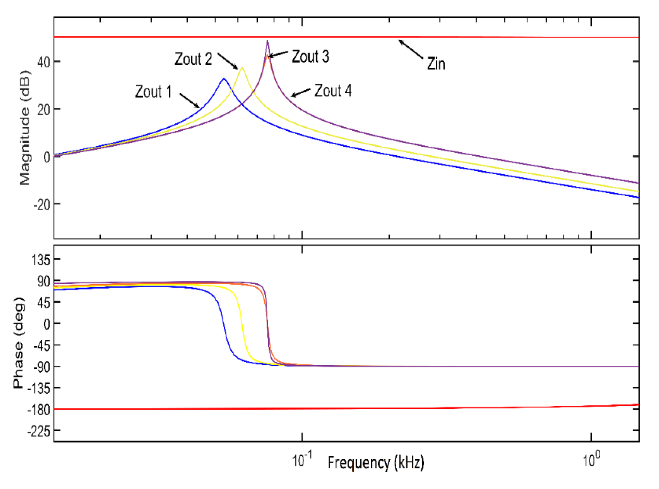
6.2. Discussion of the Stability Analysis

In this section, the results of the frequency-domain analysis are presented. Firstly, the small-signal system stability is evaluated considering the output impedances, which is the most unfavorable scenario for stability purposes. After that, another case study is carried out considering the grid as an ideal voltage source, and as a consequence, the DAB input voltage at DAB is considered stable. Therefore, according to these two assumptions, the first considers the line and DC coupling impedances (i.e., RDC, LDC, RAC and LAC). On the contrary, the second assumes an ideal DC source voltage where these impedances are neglected.
The stability can be demonstrated by overlapping Zin and the four Zout impedances in the same bode plot. In Figure 12, it is seen that the input impedance of the DAB is above all these output impedances, and the phase margin is below 90 degrees. The values of these four impedances are summarized in Table 4. The larger the resistor and capacitor, the higher are the gain margin and the more stable is the system.
To verify the previous explanation, the Nyquist diagram is displayed in Figure 13, where it can be seen that the four scenarios meet the stability criterion. As expected from the results in Figure 12, the most stable scenario occurs with Zout1, which is the closest to the origin in Figure 13. On the contrary, the less stable case occurs when Zout4 is considered.
It is worth mentioning that the parameters in both the inner and outer loops are those obtained with the GA (i.e., Kp1 = 33.55, Ki1 = 0.673, λ1 = 0.217; Kp2= 4.89; Ki2 = 18.24, λ2 = 0.32).
Once the stability of the DAB with the three-phase rectifier and the main grid has been performed, the rest of this section aims to show the performance of the parameters obtained with the three algorithms. To that purpose, as stated earlier, the main grid is now considered an ideal source and therefore, Vin can be regarded as stable. The Nyquist diagram of the closed-loop is illustrated in Figure 14, whereas the bode plot is shown in Figure 15. From Figure 14, it can be seen that all controllers will provide a stable response. Nevertheless, the relatively most stable results are expected when the controllers are tuned with the GA. On the contrary, the parameters obtained with the PSO algorithm may result in a relatively least robust response. The bode diagram depicted in Figure 15 is in accordance with the previous assertion. Lastly, the bode diagram of the open-loop transfer functions according to the current and voltage controllers are displayed in Figure 16 and Figure 17, respectively.

7. Simulation Results

7.1. Simulation Parameters

Specifications and simulation parameters of the investigated system have been summarized in Appendix A in Table A1. One set of FO-PI controllers parameters obtained from each evolutionary search algorithms is summarized in Table 5. The simulation study is carried out based on these values. The overall DC microgrid system has been implemented in the PSIM software package, where the load models are displayed in Figure 18.

7.2. Loading Conditions and Testing Scenarios

The time-domain simulations carried out with the detailed microgrid model implemented in PSIM can be divided into two major case studies. The first one tests the system’s response for a step-change in the voltage reference considering a resistive load. On the other hand, the second case study analyzes a sudden load change. Within the second case study, three types of voltage-dependent load models have been considered (i.e., constant impedance, constant power, and two types of single-phase inverters feeding R and RL loads) as illustrated in Figure 18. The modelled single-phase inverters have been designed to work in two modes. The first inverter operates in square wave mode, whereas the second is a bipolar SPWM.
The responses obtained for each set of parameters obtained according to the three evolutionary algorithms are discussed and analyzed in Section 7.3, Section 7.4 and Section 7.5, for several load models. The optimization data is analyzed in Section 7.6, whilst a quantitative analysis of the DC microgrid performance is summarized in Table 6.

7.3. System Response Considering a Resistive Load

Initially, the microgrid is loaded with a constant resistive load of 20 Ω. The voltage reference is set to 100 V, and at t = 0.1 s, the reference is changed to 200 V. The response of the DC bus voltage and the corresponding DC bus current are illustrated in Figure 19a, Figure 20a and Figure 21a according to the FO-controllers tuned by PSO, SA and GA, respectively. Based on the obtained results, the FO-PI controllers tuned by the evolutionary search algorithm result in a satisfactory transient response of the microgrid DC bus voltage.
Secondly, the microgrid is subjected to a sudden load change, where the load resistance is increased from 20 Ω to 10 Ω. Meanwhile, the DC bus voltage reference is kept fixed to 200 V. The load disturbance occurs at t = 0.15 s as shown in Figure 19b, Figure 20b and Figure 21b for PSO, SA and GA, respectively.
The voltages displayed in these figures indicate that the FO-PI controllers tuned by GA and SA algorithms provide a smoother response than those obtained by the PSO algorithm. The percentage of steady-state errors during the microgrid load change are 0.7%, 0.9%, and 1.26% with FO-controllers tuned by GA, SA, and PSO algorithms, respectively.
In addition, the voltage response obtained for the three algorithms is depicted in Figure 22, where the three evolutionary search algorithms result in a similar transient response. Moreover, the peak overshoot is less than 3% for the three algorithms. Therefore, this event cannot yet be used as a determining factor to select the best tuning strategy.
As shown in the comparison displayed in Figure 23, the controllers tuned by GA and SA cause a voltage dip of 3.75 V and 4.5 V, respectively. Meanwhile, the PSO leads to a larger voltage dip, 7.5 V. Consequently, it has been demonstrated that the relatively best dynamic response is achieved with the parameters tuned by the GA in terms of voltage stability and steady-state error. In contrast, the worst response is obtained with the parameters tuned by the PSO.

7.4. System Response Considering a Constant Power Load

In this operating scenario, the DC microgrid is loaded with a constant power load with an initial power of 1 kW. At t = 0.3 s, the load power is abruptly changed to 2 kW. The corresponding system responses (i.e., the DC voltage and current) are plotted in Figure 24 for the FO-controllers tuned by PSO, SA, and GA algorithms, respectively.
The obtained results prove that the FO controllers provide a robust response in terms of voltage stability when a constant power load increase is considered. If the FO-PI controllers tuned by PSO are analyzed, the obtained voltage drop is 1.5 V, representing a 0.75% deviation. Meanwhile, the voltage dips are 1.3 V and 0.3 V for the SA and GA, respectively. As can be observed, the FO-PI controllers tuned by the GA provide the relatively best response in terms of voltage regulation.

7.5. Response with Single-Phase Inverters

The investigated microgrid system has been tested considering AC loads feed by single-phase inverters. In practice, these inverters can be used in many applications (e.g., including pumping systems, ventilators and air conditioning systems). In this study, two operating scenarios have been presented. In the first scenario, the inverter operates in square-wave mode, producing a fixed output voltage waveform. In the second operating scenario, the inverter is working in a bipolar-SPWM mode, where the output voltage of the inverter can be controlled by adjusting the amplitude modulation index.

7.5.1. Square-Wave Single-Phase Inverter

In this subsection, the response of the DC bus voltage is illustrated with the three sets of FO-PI controller parameters. Initially, the inverter is loaded with a resistance of 60 Ω, which at = 0.25 s it is reduced to 20 Ω. The inverter operating frequency is 60 Hz (i.e., the fundamental frequency).
The response of the microgrid has been illustrated in Figure 25, Figure 26 and Figure 27 with the controllers’ parameters tuned by PSO, SA and GA, respectively. The voltage drop during the sudden load variation proved to be 198.4 V if the controller parameters tuned by the PSO are considered, which is a deviation of 0.8% with respect to the rated DC voltage.
In Figure 25a, the inverter output current is plotted, while the resultant bus voltage is plotted in Figure 25b. The inverter output voltage is also displayed in Figure 25c.
If the SA algorithm tune the FO-PI controllers, the voltage drop caused by the load change is 198.9 V, that is, a 0.55% decrease. Figure 26a,b show the inverter current and the DC bus voltage, respectively. Moreover, the inverter voltage is illustrated in Figure 26c.
If the obtained FO-PI controller parameters obtained by the GA are considered, the bus voltage decreased to 199.7 V during the sudden load variation, representing a voltage drop of 0.15% with respect to the rated value. The inverter output current is presented in Figure 27a. On the other hand, the resultant bus voltage is plotted in Figure 27b, and the inverter output voltage is displayed in Figure 27c.
According to the obtained results, the FO-controller parameters tuned by the GA algorithm exhibit the minimum voltage drop during the load resistance change if the single-phase inverter operates in square-wave mode. In contrast, the relatively worst result has been achieved with PSO algorithm.

7.5.2. SPWM Single-Phase Inverter

The response of the DC bus voltage is illustrated in this section for the three sets of FO-PI controller parameters considering an SPWM single-phase inverter. Initially, the inverter is loaded with an RL load whose resistive and inductive values are 60 Ω and 2 mH, respectively. Afterwards, at t = 0.25 s, the resistive term is reduced to 20 Ω. The inverter operating frequency is 60 Hz, the switching frequency is 15 kHz and the amplitude modulation index 0.6.
The response of the microgrid has been illustrated in Figure 28, Figure 29 and Figure 30 with controllers’ parameters tuned by PSO, SA and GA, respectively.
During the transient caused by the sudden load connection, a negligible overvoltage has been identified with the parameters tuned by the PSO algorithm (200.3 V). Whereas, during the same event, the minimum recorded voltage value proved to be 198.6 V. The maximum peak-to-peak voltage ripple is 1.7 V, representing a 0.85% drop with respect to the rated voltage. In Figure 28a, the inverter output current is plotted, while the resultant Bus voltage is plotted in Figure 28b. In addition, the corresponding spectral decomposition of the DC bus voltage is plotted in Figure 28c. According to the obtained results of the spectral decomposition, the ripple of the DC bus voltage has a low-order harmonic content with negligible magnitudes.
When the parameters tuned by the SA are considered, a negligible overvoltage has been measured during the transient caused by the load connection, see Figure 28a. Whereas, during the same event, the minimum voltage value proved to be 199.2 V. The maximum peak-to-peak voltage ripple is 1.5 V, representing a 0.75% drop with respect to the rated voltage. Figure 29a shows that the inverter output current is plotted, while the resultant DC bus voltage is plotted in Figure 29b.
In addition, the corresponding spectral decomposition of the DC bus voltage is plotted in Figure 29c. According to the obtained results of this decomposition, it is seen that the ripple of the DC bus voltage has a low-order harmonic content with negligible magnitudes. In particular, a second-order harmonic content with a magnitude of 0.109 V is observed.
When the tuned parameters are obtained with the GA algorithm, the maximum over-voltage observed during the transient caused by the sudden load connection is 203 V (see Figure 30a). On the contrary, during the same event, the minimum voltage value proved to be 198.1 V. The maximum peak-to-peak voltage ripple is 4.9 V, representing a 2.45% drop with respect to the rated voltage.
In Figure 30a, the inverter output current is plotted, while the resultant Bus voltage is plotted in Figure 30b. In addition, the corresponding spectral decomposition of the dc bus voltage is plotted in Figure 30c.
It has been observed that if an SPWM inverter is selected to fed AC loads through the DC link, the worst achieved results in terms of peak-to-peak voltage ripple are those tuned by the GA algorithm, see the plots in Figure 30.
Considering the above, the proportional gain of the voltage controller is relatively large (i.e., Kp1 33.55) compared with the corresponding values achieved by the two other algorithms (i.e., Kp1 with PSO is 9.4 and Kp1 with SA is 16.3).
Accordingly, this gain is intentionally reduced to 30 and the response has been investigated again. The archived results of the DC bus voltage, current and, the corresponding spectral decomposition are plotted again in Figure 31a,b respectively.
Considering this change in the value of Kp1, the maximum detected bus voltage is 201.7 V, while the minimum detected value is 198.4 V. Thus, the peak-to-peak voltage ripple became 3.3 V instead of 4.9 V.
According to resultant spectral decomposition, the DC bus voltage has a low order harmonic content. Thus, a slight second-order harmonic component with 0.077 V magnitude is observed.

7.6. Results of the Optimization Process

The principal comparison items in this section are the following; the convergence time of each algorithm and the steady-state value of the objective function. The evolution of fitness function has also been considered as a critical factor for comparison purposes. Accordingly, the results of the convergence are provided in Figure 32, where it is seen that all algorithms converge to the same minimum final value. However, the GA algorithm converges to the final solution after 10 iterations, the PSO algorithm after 18 iterations, while the SA algorithm’s convergence is achieved in 40 iterations. The time of convergence for each algorithm is summarized in Table 6. Although the GA algorithm converges to the optimal solution with fewer iterations than the other considered algorithms, the overall convergence time is the largest when compared with the PSO and SA.
Crucially, it has been found that SA is the fastest algorithm; meanwhile, GA is the one the takes more time for each iteration. The elapsed time for each iteration in the GA algorithm is between 10 s and 12 s, between 4 s and 6 s for the PSO and between 0.5 s and 1 s for the SA.

7.7. Impact of Parameters Uncertainty on the DC Bus Voltage

The impact of parameters variation on the DC bus voltage has been studied and summarized in this subsection. Besides load variation, four uncertain parameters have been considered in this article (leakage inductance Lk, inductor equivalent series resistance Rk, DAB input capacitance C1, and DAB output capacitance C2). The impact of parameters variation is studied considering a single-phase inverter operating in square-wave mode with an AC load.
The inductance (Lk) is subjected to ± 30% variation from the nominal value (170 μH). The resultant voltage dips under the extreme values have been listed in Table 7. The results indicate that the Lk uncertainty has a negligible effect on the DC bus voltage.
Secondly, as shown in Table 8, two additional ESR (Rk) values have been considered (i.e., 0.05 Ω and 1 Ω). The resultant voltage drops with these different ESR values are summarized in Table 8. The results indicate that the Rk has a negligible effect on the DC bus voltage.
Thirdly, the DAB capacitances (C1) and (C2) have been subjected to a ±25% variation with respect to their rated value, that is, 400 μF. The resultant voltage drops for these case studies are provided in Table 9 and Table 10. The results indicate that both C1 and C2 have no noticeable effect on the DC bus voltage. The results summarized in Table 6, Table 7, Table 8, Table 9 and Table 10 indicate that the microgrid load is the most dominant uncertain parameter; meanwhile, as mentioned above, the other passive parameters of the DAB have negligible impact on the DC bus voltage of the microgrid.

8. Comparison with Other Existing Techniques

This article has analyzed three evolutionary algorithms to tune the FO-PI controllers of a DAB for voltage stability purposes in a DC microgrid. The following comparison highlights the contribution of our assessment:
  • In the available literature, several recent articles have used evolutionary algorithms to obtain optimal parameters in many applications, see [42,43,44,45,46,47,48]. However, any of them has been used to tune FO-PI controllers for voltage stability purposes in DC microgrids. Moreover, most of them have only used one algorithm. On the contrary, in the present paper, a comparison between three different algorithms is provided.
  • Although the recently published articles towards voltage stability in DC microgrids have considered innovative approaches to address several drawbacks, they have assumed the controller parameters a fixed value without considering the optimal tuning process. For instance, see [24,25,26,27,28,29].
Lastly, it is worth mentioning that the proposed assessment has provided a robust response for voltage stability through optimal FO-PI controller parameters, enhancing the current status within this field.

9. Conclusions

In this paper, three evolutionary optimization algorithms have been used to tune the FO-PI controllers implemented in a DAB-based DC microgrid. The aim is to find the optimal parameters for these controllers in terms of voltage stability.
Firstly, the DAB small-signal model has been used for the offline optimization process. Once the three sets of optimal parameters are obtained, a frequency-domain analysis model has been developed to predict the voltage stability of the DC microgrid using the passivity-based criterion.
It has been observed that the microgrid controllers with the obtained three sets of parameters for each algorithm meet the Nyquist criterion, and therefore, stable responses are expected. However, as seen in Section 6, the most stable scenario occurs with the parameters tuned with the GA and the less stable with the PSO algorithm.
To verify such analysis, the detailed model of the DC microgrid has been implemented in PSIM software, where the time-domain simulations are performed. These simulations have been carried out considering several test cases, including changes in the voltage reference and sudden load changes. Hence, as shown in Figure 23 of Section 7, the best dynamic response is achieved by the GA, whereas the least one occurs with the PSO. Thereby, the dependability of the stability analysis provided in Section 7 has been demonstrated. Moreover, it has also been found that the GA provides the lowest voltage ripple during the tested events.
In terms of computation, the GA algorithm is the one that takes more time for each iteration to converge, but the final overall time convergence is roughly 1.5 min, which is between SA and PSO.
By observing the features comparison contained in Table 6, it can be concluded that the GA is the algorithm that offers the best performance for voltage stability as well as an acceptable computation time.
Finally, the influence of the passive parameters of the DAB has also been analyzed. The results summarized in Table 6, Table 7, Table 8, Table 9 and Table 10 indicate that elements such as the DAB leakage inductor or DC link capacitances have no noticeable impact on the DC bus voltage. Therefore, it has been demonstrated that both the microgrid load model and its composition are the dominant parameters in the voltage stability assessment.

Author Contributions

Conceptualization, M.A.; methodology, M.A. and A.S.-F.; software, M.A.; formal analysis, M.A.; investigation, M.A. and A.S.-F.; stability assessment, A.S.-F.; writing—original draft preparation, M.A.; writing and editing, M.A. and A.S.-F.; revision on first draft M.A. and S.A; final revisions M.A.; A.S.-F. All authors have read and agreed to the published version of the manuscript.

Funding

This research did not receive any external funding.

Conflicts of Interest

The authors declare no conflict of interest.

Abbreviations

CPLConstant power load
DABDual Active Bridge
DCDirect Current
ESREquivalent series resistance of inductor Lk
FOFractional Order
GAGenetic Algorithm
HFLHigh Frequency Link
PSOParticle Swarm Optimization
SASimulated Annealing
SPSMSingle Phase Shift Modulation
PFPower Factor
PIDProportional Integral Derivative Controller
PIProportional Integral Controller
PVPhotovoltaic
VSIVoltage Source Inverter
1-ϕSingle Phase
TPSTriple Phase Shift

Nomenclatures

LkLeakage inductance of inductor
RkESR of inductor Lk
KpProportional gain of conventional PID controller
KiIntegral gain of conventional PID controller
KdDifferentiator gain of conventional PID controller
e (t) Error signal between reference and actual signals
u(t) Output of PID controller
Kp1Gain of proportional term of FO-voltage controller
Ki1Gain of integral term of FO-voltage controller
λ1Order of integral term of FO-voltage controller
Kp2Gain of proportional term of FO-current controller
Ki2Gain of integral term of FO-current controller
λ2Order of integral term of FO-current controller
ϕPhase shift
dPhase shift ratio
PoAverage output power of DAB converter
fsInverter switching frequency
G p i d Transfer function of conventional PID controller
G f o c Transfer function of fractional order controller
TTemperature parameter of SA algorithm
VDC DC bus voltage
vpPrimary voltage of HF transformer
vSSecondary voltage of HF transformer
nTurns ratio of HF Transformer
JObjective function of evolutionary algorithm
JPSOObjective function of PSO algorithm
JSAObjective function of SA algorithm
JGAObjective function of GA algorithm
wInertia weight of PSO algorithm
α , β random numbers
kIteration number k of the PSO algorithm
iParticle number i of the PSO algorithm
GGlobal best position found by all particles
LLocal (Particle) best position
LSInductance of the AC link inductor
RSEquivalent resistance of the AC link inductor
v i k Velocity of the particle i at iteration k
n,cNeighborhood and current solutions in SA

Appendix A

Table A1. Specifications and simulation parameters of the investigated system.
ParameterValue
PC capability
ProcessorIntel core i3 CPU 1.7 GHz
Ram8 GB
Simulation PlatformMatlab R2014a
PSIM® Professional version 9.0.3
AC Grid3-Phase AC Grid
Grid line voltage380 V/50 HZ
DC impedanceRDC = 0.35 Ω and LDC = 6 mH
DAB Inductor
Leakage inductor (Lk)170 μH
ESR of Lk (Rk)0.2 Ω
HFL Transformer
Turns ratio2:1 (step down)
DC Bus
Rated Voltage200 V
Inverter Power Device
TypeIGBT Branch Module
Rating1200 V/75 A
Filter Capacitors
Input Capacitor C1400 μF
Output Capacitor C2400 μF
Simulation sampling time10 μs
DAB switching frequency25 kHz

References

  1. Hou, N.; Li, Y.W. Overview and Comparison of Modulation and Control Strategies for a Nonresonant Single-Phase Dual-Active-Bridge DC–DC Converter. IEEE Trans. Power Electron. 2020, 35, 3148–3172. [Google Scholar] [CrossRef]
  2. Sun, X.; Wang, H.; Qi, L.; Liu, F. Research on Single-Stage High-Frequency-Link SST Topology and Its Optimization Control. IEEE Trans. Power Electron. 2020, 35, 8701–8711. [Google Scholar] [CrossRef]
  3. Xia, P.; Shi, H.; Wen, H.; Bu, Q.; Hu, Y.; Yang, Y. Robust LMI-LQR Control for Dual-Active-Bridge DC–DC Converters with High Parameter Uncertainties. IEEE Trans. Transp. Electrif. 2020, 6, 131–145. [Google Scholar] [CrossRef]
  4. Liu, P.; Duan, S. A Hybrid Modulation Strategy Providing Lower Inductor Current for the DAB Converter with the Aid of DC Blocking Capacitors. IEEE Trans. Power Electron. 2019, 35, 4309–4320. [Google Scholar] [CrossRef]
  5. Hou, N.; Song, W.; Li, Y.W.; Zhu, Y.; Zhu, Y. A Comprehensive Optimization Control of Dual-Active-Bridge DC–DC Converters Based on Unified-Phase-Shift and Power-Balancing Scheme. IEEE Trans. Power Electron. 2018, 34, 826–839. [Google Scholar] [CrossRef]
  6. Hebala, O.M.; Aboushady, A.A.; Ahmed, K.H.; Abdelsalam, I.A. Generic Closed-Loop Controller for Power Regulation in Dual Active Bridge DC–DC Converter with Current Stress Minimization. IEEE Trans. Ind. Electron. 2019, 66, 4468–4478. [Google Scholar] [CrossRef]
  7. Liu, Y.; Wang, X.; Qian, W.; Janabi, A.; Wang, B.; Lu, X.; Zou, K.; Chen, C.; Peng, F.Z. A Simple Phase-Shift Modulation Using Parabolic Carrier for Dual Active Bridge DC–DC Converter. IEEE Trans. Power Electron. 2020, 35, 7729–7734. [Google Scholar] [CrossRef]
  8. Voss, J.; Engel, S.P.; De Doncker, R.W. Control Method for Avoiding Transformer Saturation in High-Power Three-Phase Dual-Active Bridge DC–DC Converters. IEEE Trans. Power Electron. 2020, 35, 4332–4341. [Google Scholar] [CrossRef]
  9. Kwak, B.; Kim, M.; Kim, J. Inrush current reduction technology of DAB converter for low-voltage battery systems and DC bus connections in DC microgrids. IET Power Electron. 2020, 13, 1528–1536. [Google Scholar] [CrossRef]
  10. Chen, L.; Shao, S.; Xiao, Q.; Tarisciotti, L.; Wheeler, P.W.; Dragicevic, T. Model Predictive Control for Dual-Active-Bridge Converters Supplying Pulsed Power Loads in Naval DC Micro-Grids. IEEE Trans. Power Electron. 2020, 35, 1957–1966. [Google Scholar] [CrossRef]
  11. An, F.; Song, W.; Yu, B.; Yang, K. Model Predictive Control with Power Self-Balancing of the Output Parallel DAB DC–DC Converters in Power Electronic Traction Transformer. IEEE J. Emerg. Sel. Top. Power Electron. 2018, 6, 1806–1818. [Google Scholar] [CrossRef]
  12. An, F.; Song, W.; Yang, K. Direct power control of dual-active-bridge dc–dc converters based on unified phase shift control. J. Eng. 2019, 2019, 2180–2184. [Google Scholar] [CrossRef]
  13. Song, W.; Hou, N.; Wu, M. Virtual Direct Power Control Scheme of Dual Active Bridge DC–DC Converters for Fast Dynamic Response. IEEE Trans. Power Electron. 2018, 33, 1750–1759. [Google Scholar] [CrossRef]
  14. Shan, Z.; Jatskevich, J.; Iu, H.H.-C.; Fernando, T. Simplified Load-Feedforward Control Design for Dual-Active-Bridge Converters with Current-Mode Modulation. IEEE J. Emerg. Sel. Top. Power Electron. 2018, 6, 2073–2085. [Google Scholar] [CrossRef]
  15. Wang, D.; Nahid-Mobarakeh, B.; Emadi, A. Second Harmonic Current Reduction for a Battery-Driven Grid Interface with Three-Phase Dual Active Bridge DC–DC Converter. IEEE Trans. Ind. Electron. 2019, 66, 9056–9064. [Google Scholar] [CrossRef]
  16. Zengin, S.; Boztepe, M. A Novel Current Modulation Method to Eliminate Low-Frequency Harmonics in Single-Stage Dual Active Bridge AC–DC Converter. IEEE Trans. Ind. Electron. 2020, 67, 1048–1058. [Google Scholar] [CrossRef]
  17. Datta, A.J.; Ghosh, A.; Zare, F.; Rajakaruna, S. Bidirectional power sharing in an ac/dc system with a dual active bridge converter. IET Gener. Transm. Distrib. 2019, 13, 495–501. [Google Scholar] [CrossRef]
  18. Shao, S.; Jiang, M.; Ye, W.; Li, Y.; Zhang, J.; Sheng, K. Optimal Phase-Shift Control to Minimize Reactive Power for a Dual Active Bridge DC–DC Converter. IEEE Trans. Power Electron. 2019, 34, 10193–10205. [Google Scholar] [CrossRef]
  19. Wu, J.; Wen, P.; Sun, X.; Yan, X. Reactive Power Optimization Control for Bidirectional Dual-Tank Resonant DC–DC Converters for Fuel Cells Systems. IEEE Trans. Power Electron. 2020, 35, 9202–9214. [Google Scholar] [CrossRef]
  20. Gu, Q.; Yuan, L.; Nie, J.; Sun, J.; Zhao, Z. Current Stress Minimization of Dual-Active-Bridge DC–DC Converter Within the Whole Operating Range. IEEE J. Emerg. Sel. Top. Power Electron. 2019, 7, 129–142. [Google Scholar] [CrossRef]
  21. Vuyyuru, U.; Maiti, S.; Chakraborty, C. Active Power Flow Control between DC Microgrids. IEEE Trans. Smart Grid 2019, 10, 5712–5723. [Google Scholar] [CrossRef]
  22. Jeung, Y.C.; Lee, D.C. Voltage and Current Regulations of Bidirectional Isolated Dual-Active-Bridge DC–DC Converters Based on a Double-Integral Sliding Mode Control. IEEE Trans. Power Electron. 2019, 34, 6937–6946. [Google Scholar] [CrossRef]
  23. You, J.; Vilathgamuwa, M.; Ghasemi, N. DC bus voltage stability improvement using disturbance observer feedforward control. Control. Eng. Pr. 2018, 75, 118–125. [Google Scholar] [CrossRef]
  24. Jeung, Y.C.; Lee, D.C.; Dragicevic, T.; Blaabjerg, F. Design of Passivity-Based Damping Controller for Suppressing Power Oscillations in DC Microgrids. IEEE Trans. Power Electron. 2021, 36, 4016–4028. [Google Scholar] [CrossRef]
  25. Li, X.; Guo, L.; Zhang, S.; Wang, C.; Li, Y.W.; Chen, A.; Feng, Y. Observer-Based DC Voltage Droop and Current Feed-Forward Control of a DC Microgrid. IEEE Trans. Smart Grid 2018, 9, 5207–5216. [Google Scholar] [CrossRef]
  26. Chen, L.; Gao, F.; Shen, K.; Wang, Z.; Tarisciotti, L.; Wheeler, P.; Dragicevic, T. Predictive Control Based DC Microgrid Stabilization with the Dual Active Bridge Converter. IEEE Trans. Ind. Electron. 2020, 67, 8944–8956. [Google Scholar] [CrossRef]
  27. Ye, Q.; Mo, R.; Li, H. Impedance Modeling and DC Bus Voltage Stability Assessment of a Solid-State-Transformer-Enabled Hybrid AC–DC Grid Considering Bidirectional Power Flow. IEEE Trans. Ind. Electron. 2019, 67, 6531–6540. [Google Scholar] [CrossRef]
  28. Bosich, D.; Vicenzutti, A.; Grillo, S.; Sulligoi, G. A Stability Preserving Criterion for the Management of DC Microgrids Supplied by a Floating Bus. Appl. Sci. 2018, 8, 2102. [Google Scholar] [CrossRef] [Green Version]
  29. Feng, F.; Zhang, X.; Zhang, J.; Gooi, H.B. Stability Enhancement via Controller Optimization and Impedance Shaping for Dual Active Bridge-Based Energy Storage Systems. IEEE Trans. Ind. Electron. 2020, 68, 5863–5874. [Google Scholar] [CrossRef]
  30. Dragicevic, T.; Lu, X.; Vasquez, J.C.; Guerrero, J.M. DC Microgrids–Part I: A Review of Control Strategies and Stabilization Techniques. IEEE Trans. Power Electron. 2015, 31, 4876–4891. [Google Scholar] [CrossRef] [Green Version]
  31. Rodriguez, A.; Vazquez, A.; Lamar, D.G.; Hernando, M.M.; Sebastian, J. Different Purpose Design Strategies and Techniques to Improve the Performance of a Dual Active Bridge with Phase-Shift Control. IEEE Trans. Power Electron. 2015, 30, 790–804. [Google Scholar] [CrossRef]
  32. Liu, L.; Shan, L.; Dai, Y.; Liu, C.; Qi, Z. Improved quantum bacterial foraging algorithm for tuning parameters of fractional-order PID controller. J. Syst. Eng. Electron. 2018, 29, 166–175. [Google Scholar] [CrossRef]
  33. Meng, F.; Liu, S.; Liu, K. Design of an Optimal Fractional Order PID for Constant Tension Control System. IEEE Access 2020, 8, 58933–58939. [Google Scholar] [CrossRef]
  34. Yaghi, M.A.; Efe, M.O. H2/H∞H2/H∞-Neural-Based FOPID Controller Applied for Radar-Guided Missile. IEEE Trans. Ind. Electron. 2019, 67, 4806–4814. [Google Scholar] [CrossRef]
  35. Chen, C.L. Simulated annealing-based optimal wind-thermal coordination scheduling. IET Gener. Transm. Distrib. 2007, 1, 447. [Google Scholar] [CrossRef]
  36. Ricobbono, A.; Santi, E. Positive feedforward control of three-phase voltage source inverter for DC input bus stabilization with experimental validation. IEEE Trans. Ind. Appl. 2013, 49, 168–177. [Google Scholar] [CrossRef]
  37. Shi, H.; Sun, K.; Wu, H.; Li, Y. A Unified State-Space Modeling Method for a Phase-Shift Controlled Bidirectional Dual-Active Half-Bridge Converter. IEEE Trans. Power Electron. 2019, 35, 3254–3265. [Google Scholar] [CrossRef]
  38. Berger, M.; Kocar, I.; Fortin-Blanchette, H.; Lavertu, C. Large-signal modeling of three-phase dual active bridge converters for electromagnetic transient analysis in DC grids. J. Mod. Power Syst. Clean Energy 2019, 7, 1684–1696. [Google Scholar] [CrossRef] [Green Version]
  39. Shah, S.S.; Bhattacharya, S. A Simple Unified Model for Generic Operation of Dual Active Bridge Converter. IEEE Trans. Ind. Electron. 2019, 66, 3486–3495. [Google Scholar] [CrossRef]
  40. Cupelli, M.; Gurumurthy, S.K.; Bhanderi, S.K.; Yang, Z.; Joebges, P.; Monti, A.; De Doncker, R.W. Port Controlled Hamiltonian Modeling and IDA-PBC Control of Dual Active Bridge Converters for DC Microgrids. IEEE Trans. Ind. Electron. 2019, 66, 9065–9075. [Google Scholar] [CrossRef]
  41. Birs, I.; Muresan, C.; Nascu, I.; Ionescu, C. A Survey of Recent Advances in Fractional Order Control for Time Delay Systems. IEEE Access 2019, 7, 30951–30965. [Google Scholar] [CrossRef]
  42. Pullaguram, D.; Mishra, S.; Senroy, N.; Mukherjee, M. Design and Tuning of Robust Fractional Order Controller for Autonomous Microgrid VSC System. IEEE Trans. Ind. Appl. 2017, 54, 91–101. [Google Scholar] [CrossRef]
  43. Tolba, M.F.; Said, L.A.; Madian, A.H.; Radwan, A.G. FPGA Implementation of the Fractional Order Integrator/Differentiator: Two Approaches and Applications. IEEE Trans. Circuits Syst. I Regul. Pap. 2018, 66, 1484–1495. [Google Scholar] [CrossRef]
  44. Seo, S.-W.; Choi, H.H. Digital Implementation of Fractional Order PID-Type Controller for Boost DC–DC Converter. IEEE Access 2019, 7, 142652–142662. [Google Scholar] [CrossRef]
  45. Liu, L.; Zhang, S.; Xue, D.; Chen, Y.Q. General robustness analysis and robust fractional-order PD controller design for fractional-order plants. IET Control. Theory Appl. 2018, 12, 1730–1736. [Google Scholar] [CrossRef] [Green Version]
  46. Ren, H.P.; Fan, J.T.; Kaynak, O. Optimal Design of a Fractional-Order Proportional-Integer-Differential Controller for a Pneumatic Position Servo System. IEEE Trans. Ind. Electron. 2018, 66, 6220–6229. [Google Scholar] [CrossRef]
  47. Lino, P.; Maione, G.; Stasi, S.; Padula, F.; Visioli, A. Synthesis of fractional-order PI controllers and fractional-order filters for industrial electrical drives. IEEE/CAA J. Autom. Sin. 2017, 4, 58–69. [Google Scholar] [CrossRef] [Green Version]
  48. Zaihidee, F.M.; Mekhilef, S.; Mubin, M. Application of Fractional Order Sliding Mode Control for Speed Control of Permanent Magnet Synchronous Motor. IEEE Access 2019, 7, 101765–101774. [Google Scholar] [CrossRef]
  49. Maddahi, A.; Sepehri, N.; Kinsner, W. Fractional-Order Control of Hydraulically Powered Actuators: Controller Design and Experimental Validation. IEEE/ASME Trans. Mechatron. 2019, 24, 796–807. [Google Scholar] [CrossRef]
  50. Crespo, T.; Duarte, M.A.; Ceballos, G.; Lefranc, G. Fractional Order Controllers for Back-to-Back Converters. IEEE Lat. Am. Trans. 2018, 16, 2427–2434. [Google Scholar] [CrossRef]
  51. Wan, J.; He, B.; Wang, D.; Yan, T.; Shen, Y. Fractional-Order PID Motion Control for AUV Using Cloud-Model-Based Quantum Genetic Algorithm. IEEE Access 2019, 7, 124828–124843. [Google Scholar] [CrossRef]
  52. Sathishkumar, P.; Selvaganesan, N. Fractional Controller Tuning Expressions for a Universal Plant Structure. IEEE Control. Syst. Lett. 2018, 2, 345–350. [Google Scholar] [CrossRef]
  53. Hekimoglu, B. Optimal Tuning of Fractional Order PID Controller for DC Motor Speed Control via Chaotic Atom Search Optimization Algorithm. IEEE Access 2019, 7, 38100–38114. [Google Scholar] [CrossRef]
  54. Mishra, A.K.; Das, S.R.; Ray, P.K.; Mallick, R.K.; Mohanty, A.; Mishra, D.K. PSO-GWO Optimized Fractional Order PID Based Hybrid Shunt Active Power Filter for Power Quality Improvements. IEEE Access 2020, 8, 74497–74512. [Google Scholar] [CrossRef]
  55. Lyden, S.; Haque, E. A Simulated Annealing Global Maximum Power Point Tracking Approach for PV Modules Under Partial Shading Conditions. IEEE Trans. Power Electron. 2016, 31, 4171–4181. [Google Scholar] [CrossRef]
  56. Delahaye, D.; Chaimatanan, S.; Mongeau, M. Simulated Annealing: From Basics to Applications. In Handbook of Metaheuristics; Gendreau, M., Potvin, J.Y., Eds.; Springer: Berlin/Heidelberg, Germany, 2019. [Google Scholar]
  57. Corus, D.; Oliveto, P.S. Standard Steady State Genetic Algorithms Can Hillclimb Faster Than Mutation-Only Evolutionary Algorithms. IEEE Trans. Evol. Comput. 2017, 22, 720–732. [Google Scholar] [CrossRef] [Green Version]
  58. Wang, Z.; Li, J.; Fan, K.; Ma, W.; Lei, H. Prediction Method for Low Speed Characteristics of Compressor Based on Modified Similarity Theory with Genetic Algorithm. IEEE Access 2018, 6, 36834–36839. [Google Scholar] [CrossRef]
  59. Mohammadi, A.; Asadi, H.; Mohamed, S.; Nelson, K.; Nahavandi, S. Multiobjective and Interactive Genetic Algorithms for Weight Tuning of a Model Predictive Control-Based Motion Cueing Algorithm. IEEE Trans. Cybern. 2019, 49, 3471–3481. [Google Scholar] [CrossRef] [PubMed]
  60. Han, C.; Wang, L.; Zhang, Z.; Xie, J.; Xing, Z. A Multi-Objective Genetic Algorithm Based on Fitting and Interpolation. IEEE Access 2018, 6, 22920–22929. [Google Scholar] [CrossRef]
  61. Yang, H.; Qi, J.; Miao, Y.; Sun, H.; Li, J. A New Robot Navigation Algorithm Based on a Double-Layer Ant Algorithm and Trajectory Optimization. IEEE Trans. Ind. Electron. 2018, 66, 8557–8566. [Google Scholar] [CrossRef] [Green Version]
  62. Ma, Y.N.; Gong, Y.J.; Xiao, C.F.; Gao, Y.; Zhang, J. Path Planning for Autonomous Underwater Vehicles: An Ant Colony Algorithm Incorporating Alarm Pheromone. IEEE Trans. Veh. Technol. 2019, 68, 141–154. [Google Scholar] [CrossRef]
  63. Zhang, Y.H.; Gong, Y.; Chen, W.N.; Gu, T.L.; Yuan, H.Q.; Zhang, J. A Dual-Colony Ant Algorithm for the Receiving and Shipping Door Assignments in Cross-Docks. IEEE Trans. Intell. Transp. Syst. 2018, 20, 2523–2539. [Google Scholar] [CrossRef]
  64. Lee, J.H.; Song, J.Y.; Kim, D.W.; Kim, J.W.; Kim, Y.J.; Jung, S.Y. Particle Swarm Optimization Algorithm with Intelligent Particle Number Control for Optimal Design of Electric Machines. IEEE Trans. Ind. Electron. 2018, 65, 1791–1798. [Google Scholar] [CrossRef]
  65. Azab, M. Multi-objective design approach of passive filters for single-phase distributed energy grid integration systems using particle swarm optimization. Energy Rep. 2020, 6, 157–172. [Google Scholar] [CrossRef]
  66. Liu, Z.H.; Wei, H.L.; Zhong, Q.C.; Liu, K.; Xiao, X.S.; Wu, L.H. Parameter Estimation for VSI-Fed PMSM Based on a Dynamic PSO With Learning Strategies. IEEE Trans. Power Electron. 2016, 32, 3154–3165. [Google Scholar] [CrossRef] [Green Version]
  67. Azab, M. Design approach and performance analysis of trap filter for three-phase PV grid integration systems using evolutionary search algorithms. J. King Saud Univ. Eng. Sci. 2020. [Google Scholar] [CrossRef]
  68. Sebtahmadi, S.S.; Azad, H.B.; Kaboli, S.H.A.; Islam, D.; Mekhilef, S. A PSO-DQ Current Control Scheme for Performance Enhancement of Z-Source Matrix Converter to Drive IM Fed by Abnormal Voltage. IEEE Trans. Power Electron. 2017, 33, 1666–1681. [Google Scholar] [CrossRef]
  69. Sarker, K.; Chatterjee, D.; Goswami, S.K. Modified harmonic minimisation technique for doubly fed induction generators with solar-wind hybrid system using biogeography-based optimisation. IET Power Electron. 2018, 11, 1640–1651. [Google Scholar] [CrossRef]
  70. Pietilainen, K.; Harnefors, L.; Petersson, A.; Nee, H.P. DC-Link Stabilization and Voltage Sag Ride-Through of Inverter Drives. IEEE Trans. Ind. Electron. 2006, 53, 1261–1268. [Google Scholar] [CrossRef]
  71. Mueller, J.A.; Kimball, J.W. Modeling Dual Active Bridge Converters in DC Distribution Systems. IEEE Trans. Power Elec tron. 2018, 34, 5867–5879. [Google Scholar] [CrossRef]
  72. Tian, Y.; Peng, F.; Wang, Y.; Chen, Z. Coordinative impedance damping control for back-to-back converter in solar power integration system. IET Renew. Power Gener. 2019, 13, 1484–1492. [Google Scholar] [CrossRef]
  73. Zhao, N.; Liu, J.; Ai, Y.; Yang, J.; Zhang, J.; You, X. Power-Linked Predictive Control Strategy for Power Electronic Traction Transformer. IEEE Trans. Power Electron. 2020, 35, 6559–6571. [Google Scholar] [CrossRef]
  74. Chen, L.; Lin, L.; Shao, S.; Gao, F.; Wang, Z.; Wheeler, P.W.; Dragicevic, T. Moving Discretized Control Set Model-Predictive Control for Dual-Active Bridge with the Triple-Phase Shift. IEEE Trans. Power Electron. 2020, 35, 8624–8637. [Google Scholar] [CrossRef]
Figure 1. Block diagram of a closed loop control system with PID controller.
Electronics 10 01109 g001
Figure 2. (λ-μ) plane of fractional order PID controller.
Electronics 10 01109 g002
Figure 3. Block diagram of the test system.
Electronics 10 01109 g003
Figure 4. Circuit diagram of the investigated system.
Electronics 10 01109 g004
Figure 5. Averaged-model of the DAB converter.
Electronics 10 01109 g005
Figure 6. The small-signal model of the DAB converter.
Electronics 10 01109 g006
Figure 7. Dual loop control of microgrid DC bus voltage.
Electronics 10 01109 g007
Figure 8. Flowchart implemented for the PSO algorithm.
Electronics 10 01109 g008
Figure 9. Flowchart implemented for the SA algorithm.
Electronics 10 01109 g009
Figure 10. Flowchart implemented for the GA algorithm.
Electronics 10 01109 g010
Figure 11. Impedance model.
Electronics 10 01109 g011
Figure 12. Bode diagram of the input and output impedances.
Electronics 10 01109 g012
Figure 13. Nyquist diagram of the resulting Zout//Zin impedances.
Electronics 10 01109 g013
Figure 14. Nyquist diagram of the closed loop transfer function for the three evolutionary algorithms.
Electronics 10 01109 g014
Figure 15. Bode diagram of the closed-loop transfer function for the three evolutionary algorithms.
Electronics 10 01109 g015
Figure 16. Bode diagram of current FO-PI controller for the three evolutionary algorithms.
Electronics 10 01109 g016
Figure 17. Bode diagram of voltage FO-PI controller for the three evolutionary algorithms.
Electronics 10 01109 g017
Figure 18. Different load models investigated in the DC microgrid.
Electronics 10 01109 g018
Figure 19. Simulation results with the PSO. (a) Change in voltage reference, (b) sudden load change.
Electronics 10 01109 g019
Figure 20. Simulation results with the SA. (a) Change in voltage reference, (b) sudden load change.
Electronics 10 01109 g020
Figure 21. Simulation results with the GA. (a) Change in voltage reference, (b) sudden load change.
Electronics 10 01109 g021
Figure 22. Comparison between the three algorithms given a step-change in voltage reference.
Electronics 10 01109 g022
Figure 23. Voltage transient response obtained during a step-change in the load resistance.
Electronics 10 01109 g023
Figure 24. Simulation results for a CPL model for the three algorithms (a) PSO, (b) SA and (c) GA.
Electronics 10 01109 g024aElectronics 10 01109 g024b
Figure 25. Microgrid response under non-linear load (square-wave inverter), (a) Inverter output current, (b) DC bus voltage, (c) Inverter output voltage in case of PSO-based tuned parameters.
Electronics 10 01109 g025
Figure 26. Microgrid response under non-linear load (square-wave inverter), (a) Inverter output current, (b) DC bus voltage, (c) Inverter output voltage in case of SA-based tuned parameters.
Electronics 10 01109 g026
Figure 27. Microgrid response under non-linear load (square-wave inverter), (a) Inverter output current, (b) DC bus voltage, (c) Inverter output voltage in case of GA-based tuned parameters.
Electronics 10 01109 g027
Figure 28. Microgrid response under non-linear load (SPWM inverter), (a) Inverter output current, (b) DC bus voltage, (c) Bus voltage spectral decomposition in case of PSO-based tuned parameters.
Electronics 10 01109 g028
Figure 29. Microgrid response under non-linear load (SPWM inverter), (a) Inverter output current, (b) DC bus voltage, (c) Bus voltage spectral decomposition in case of SA-based tuned parameters.
Electronics 10 01109 g029
Figure 30. Microgrid response under non-linear load (SPWM inverter), (a) Inverter output current, (b) DC bus voltage, (c) Bus voltage spectral decomposition in case of GA-based tuned parameters.
Electronics 10 01109 g030
Figure 31. Microgrid response under non-linear load (SPWM inverter), in case of GA-based tuned parameters (Kp1 is 30), (a) DC bus voltage, (b) Bus voltage spectral decomposition.
Electronics 10 01109 g031
Figure 32. Evolution of the fitness function for the three algorithms.
Electronics 10 01109 g032
Table 1. Parameters of the PSO algorithm.
Particles
(Birds)
Max.
Iterations
Inertia Weighting
Factor w
α,β
1001000.05Random number [0,1]
Table 2. Parameters of the SA algorithm.
Max.
Iter.
Max. Function
Evaluations
Initial Temp.Annealing Parameters
FunctionIntervalDecay
Temperature
10003000 × n100Boltzmann100Exponential
Table 3. Parameters of the GA algorithm.
PS 1Creation FunctionFitness ScalingSelectionReproductionMutationCrossover Function
Elite
Count
Crossover FractionFunctionRate
100UniformRankStochastic uniform0.05 PS0.8Uniform0.01Scattered
1 PS = Population size.
Table 4. Parameters of Zout.
-R (Ω)L (H)C (μF)
Zout10.320.011800
Zout20.250.011600
Zout30.20.011400
Zout40.10.011400
Table 5. Parameters of the FO-PI controller for each evolutionary algorithm.
AlgorithmController
Voltage ControllerCurrent Controller
ParametersParameters
Kp1Ki1λ1Kp2Ki2λ2
PSO9.40.1631.748.420.561.44
SA16.310.1554.216.850.105
GA33.550.6730.2174.8918.240.32
Table 6. Summary of the convergence and performance results for the three algorithms.
ITEMPSOSAGA
Algorithm convergenceNumber of iterations to converge184010
Iteration run time (s)4–60.5–110–12
Algorithm convergence time (min)1.2–1.80.33–0.661.66–2
Performance under linear load (Resistive)Settling time (s)0.0020.0020.002
Peak overshoot (% of reference voltage)333
Voltage ripple during load variation (%)1.260.900.70
Transient peak voltage dip (V)7.54.53.75
Performance under (CPL)Voltage dip due to sudden load change (V)1.51.30.30
Voltage dip due to sudden load change (%)0.750.650.15
Performance with a single-phase inverterVoltage dip due to sudden load change
with square-wave inverter (%)
0.80.550.15
Voltage dip due to sudden load change
with SPWM inverter (%)
0.850.752.45
1.65 *
Low-order harmonic magnitude
voltage (%)
0.0760.0540.042
0.038 *
* Kp1 is reduced from 33.55 to 30.
Table 7. Effect of Inductor Lk on the bus voltage.
AlgorithmVoltage Dip Due to Inductor Lk Uncertainty
(Lk Nominal = 170 μH)
Lk min = 120 μHLk = 170 μHLk max = 220 μH
PSO1.60 V1.63 V1.70 V
SA0.99 V1.02 V0.93
GA0.50 V0.52 V0.51
Table 8. Effect of Inductor Rk on the bus voltage.
AlgorithmVoltage Dip Due to Inductor ESR Uncertainty
(Rk Nominal = 0.2 Ω)
Rk min = 0.05 ΩRk = 0.2 ΩRk max = 1 Ω
PSO1.80 V1.63 V1.60 V
SA1.05 V1.02 V1.02 V
GA0.60 V0.52 V0.50 V
Table 9. Effect of DAB input capacitor C1 on the bus voltage.
AlgorithmVoltage Dip Due to Inductor Lk Uncertainty
(C1 Nominal = 400 μF)
C1 min = 480 μFC1 = 400 μFC1 max = 320 μF
PSO1.59 V1.63 V1.60 V
SA1.01 V1.02 V1.06 V
GA0.51 V0.518 V0.519 V
Table 10. Effect of DAB output capacitor C2 on the bus voltage.
AlgorithmVoltage Dip due to Inductor Lk Uncertainty
(C2 Nominal = 400 μF)
C2 min = 480 μFC2 = 400 μFC2 max = 320 μF
PSO1.58 V1.63 V1.68 V
SA1.00 V1.02 V1.05 V
GA0.498 V0.52 V0.541 V
Publisher’s Note: MDPI stays neutral with regard to jurisdictional claims in published maps and institutional affiliations.

