Article

Reconfigurable Distributed Power Electronics Technique for Solar PV Systems

1
Department of Energy Technology, Aalborg University, 9220 Aalborg, Denmark
2
School of Electrical Engineering & Robotics, Queensland University of Technology, Brisbane, QLD 4000, Australia
*
Author to whom correspondence should be addressed.
Electronics 2021, 10(9), 1121; https://doi.org/10.3390/electronics10091121
Submission received: 28 March 2021 / Revised: 27 April 2021 / Accepted: 7 May 2021 / Published: 10 May 2021
(This article belongs to the Special Issue Photovoltaic Energy Systems and Storage)

Abstract

:
A reconfiguration technique using a switched-capacitor (SC)-based voltage equalizer differential power processing (DPP) concept is proposed in this paper for photovoltaic (PV) systems at a cell/subpanel/panel-level. The proposed active diffusion charge redistribution (ADCR) architecture increases the energy yield during mismatch and adds a voltage boosting capability to the PV system under no mismatch by connected the available PV cells/panels in series. The technique performs a reconfiguration by measuring the PV cell/panel voltages and their irradiances. The power balancing is achieved by charge redistribution through SC under mismatch conditions, e.g., partial shading. Moreover, PV cells/panels remain in series under no mismatch. Overall, this paper analyzes, simulates, and evaluates the effectiveness of the proposed DPP architecture through a simulation-based model prepared in PSIM. Additionally, the effectiveness is also demonstrated by comparing it with existing conventional DPP and traditional bypass diode architecture.

1. Introduction

Renewable energy sources are environmentally friendly sources of clean and green energy. Renewable energy sources, hydro, solar, tidal, and wind power are continuously increasing their share in electricity production. The global estimated energy share of various renewable sources is given in Figure 1 [1]. Among these energy sources, photovoltaic (PV) technology is increasing at a much faster rate than other existing renewable sources. The continuous decline in the manufacturing cost of PV panels and the increase in solar cell efficiency is the main reason for PV technology success. For example, a steep rise in the electricity generated in Germany by PV systems has already reached around 50 GWp. Moreover, PV generation even covers the energy requirement up to 50% in Germany on some days [2].
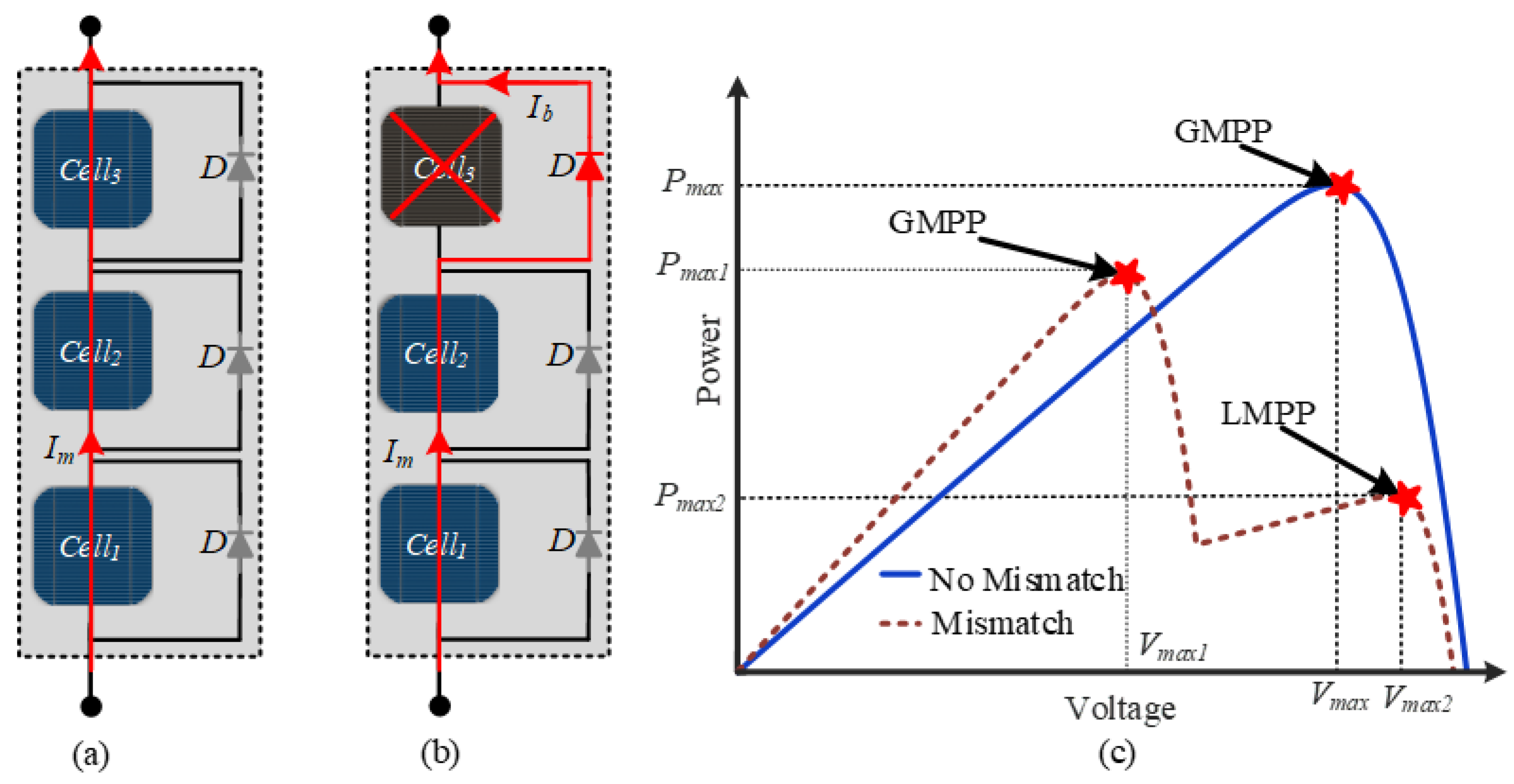
In small PV applications, several PV cells are employed in series to achieve the desire voltage level, where the current in series always remains the same. The current generation in the PV cell depends on the irradiance level. Hence, under the same irradiance level, the PV string that consists of series-connected PV cells has only a single maximum power point (MPP). Hence, the cells in the string are contributing equally to the overall string power (see Figure 2a). However, if the PV cells are subjected to a different level of irradiance within the same string, the output currents from the PV cells become unequal. The unequal currents cause a mismatch in a PV string. This mismatch phenomenon of unequal current can be caused by several factors, e.g., partial shading caused by clouds, PV cell orientations, soiling, equal or unequal aging, dirt, manufacturing differences, etc. [3].
During mismatch, the affected (shaded) PV cells generate less current than the string current. Therefore, the bypass diodes are used in parallel to PV cells or a group of series-connected cells. These bypass diodes bypass the low-power-producing cell or subpanel [4,5]. Hence, the string current starts to flow through these conducted diodes, as depicted in Figure 2b. The bypassed PV cells are shorted out. Therefore, there is no contribution from these PV cells towards the string’s output. Additionally, these bypass diodes cause multiple MPPs under mismatch due to the bypassing of low power-producing PV cells, as visualized in Figure 2c. These nonconvex output power characteristics lead to further complications for the maximum power point tracking (MPPT) algorithms in tracking the global power peak [6,7]. During mismatch, bypassed cells may become reverse-biased and start to dissipate power instead of producing power. Power dissipation increases the solar cell temperature, also known as hot-spots [8], as shown in Figure 3. These hot-spots in PV cells cause an early degradation and decrease the reliability of the overall PV system [9]. Moreover, the overall power extraction from a PV string is severely limited by mismatches, which adversely influences the long-term project economics [10].
To limit the mismatch effect in the PV system, there are static and dynamic configuration techniques. In static configurations, the position of PV cells remains the same [11]. However, they can be connected in various configurations, e.g., Series, Series-Parallel (SP) [12], Total-Cross-Tie (TCT) [13], Bridge-Linked (BL) [14] connections, etc. In dynamic configurations, the PV cells are physically rearranged in various defined orders in order to reduce the power mismatch [13]. The PV cells are arranged in such a way that the effect of shading disperses over the entire array, which improves the overall performance by yielding extra power. However, finding the best possible arrangement increases the complexity of the dynamic reconfiguration techniques due to the unnecessary global maximum power peak (GMPP) search, which also causes an efficiency reduction. Furthermore, the occurrence of partial shading in dynamic reconfiguration is usually detected using a short circuit current (Isc), which requires the load to be removed during the detection of the mismatch. Hence, this greatly affects the connected loads. In all, static, as well as dynamic, configurations are used to minimize partial shading losses.
Furthermore, there are also power electronic (PE)-based architectures to mitigate the effects of mismatches, which are presented in the literature at the PV string-, panel-, subpanel-, and cell-level, as shown in Figure 4. These PE architectures typically include microinverters, DC optimizers, and partial or differential power processing (DPP) converters. The PE converters are also known as distributed maximum power point tracking (DMPPT) converters as they track the MPP of each panel individually [15,16,17]. The main advantage of distributed power electronics (DPE) is the mitigation of mismatch effects in a PV system. Moreover, the DMPPT increases the energy yield of the overall system [18,19,20,21,22,23,24,25,26,27,28,29,30]. Additionally, DPE converters can also help in the improvement of the system reliability by reducing the hot-spots shown in Figure 3. However, the major and essential drawback of DC optimizer and microinverter architectures is the full power processing (FPP) by each PE converter. Hence, converters with full power ratings are necessary, which not only increases the losses but also the size of the PE converter.
Furthermore, DPE-based DPP architectures are an emerging mismatch mitigation technique for addressing mismatch issues by only processing the mismatched power [29,31,32]. Several DPP converters are presented in the literature, and they are also known as voltage equalizers. The partial power processing (PPP) voltage equalizers are DC-DC PE converters, which make it possible to process a small portion of the extra power stored by the energy storage element that is produced by the unshaded PV panels. The voltage equalizers or DPP converters include, buck-boost [33,34], switched-capacitor (SC) [20,35,36], isolated and non-isolated bus [37,38] DPP PE converters. However, these DPP converters require external energy storage components, e.g., inductors and capacitors. These external components make the topology size greater and the topology itself expensive. Therefore, voltage equalizer applications are very limited, and it is difficult to apply them on small PV applications at the cell level to mitigate the mismatch issues, e.g., electric cars, wearable bags, moon hovers, drones, etc.
Among these, SC-based DPP topologies have the advantage of a reduced circuit size, because the power densities of inductive elements are 100–1000 times less than those of capacitive elements [39,40]. Moreover, another capacitorless SC-based voltage equalizer DPP topology is proposed in [18]. This capacitorless DPP topology uses the internal diffusion capacitance Cd of solar cells, as shown in Figure 5a. This diffusion capacitance is a parasitic element that originates from the P-N junction of PV cells. This ladder-based capacitorless SC-based DPP topology is known as a diffusion charge redistribution (DCR) architecture, which uses the diffusion capacitance Cd of a solar cell for mismatch charge distribution. The mismatch charges are distributed by storing them in one cycle and releasing them in the next cycle. The purpose of storing the mismatch charges is to maintain the series current at a level equal to that of the current generated by a low-irradiance solar cell. Moreover, the converter works at a high switching frequency, which helps in the equalization of voltages by using diffusion capacitance Cd to extract maximum available power from each solar cell. Additionally, the DCR topology reduces the size and cost of the DPP topology. However, regardless of whether there is a mismatch or not, the DCR topology has to operate continuously at a high switching frequency, which generates unnecessary switching loss.
To add more features to the DCR voltage equalizer, a reconfigurable active diffusion charge redistribution (ADCR) technique is presented in this paper, typically for small-scale PV applications with limited size. The introduced methodology uses DCR topology by adding a reconfiguration feature. The reconfiguration feature can help the system to operate the PV cells in series under no mismatch, which also adds a boosting voltage capability to the PV system. However, under mismatch, the introduced ADCR technique uses a reconfiguration feature without isolating the load to mitigate the effect of mismatch by configuring itself to the DCR DPP converter. Therefore, in comparison to existing work [17], our contribution applies a reconfiguration using the differential power processing (DPP) converter for the first time in the literature (to the best of our knowledge). The existing DPP converter-based voltage balancing technique presented in [17] incurs excessive switching losses under no mismatch conditions due to the unnecessary switching of MOSFETS in the DPP converter. This is one of the serious drawbacks of using the conventional DCR approach, and this drawback can be mitigated by using the reconfiguration scheme proposed in this work.
The paper is organized as follows. The theoretical background of the solar cell diffusion capacitance is presented in Section 2. Section 3 presents the introduced ADCR DPP technique along with the proposed reconfiguration algorithm, and the simulated results are presented in Section 4. Finally, the conclusion is drawn in Section 5.

2. PV Cell Diffusion Capacitance

Generally, a single-diode model is used to represent PV cells, as depicted in Figure 6a. The current-voltage (I-V) characteristics of the solar cell according to this commonly used single-diode model can be expressed as [18]:
I s = I s c I d V d R s h
where Is is the solar cell current, Id is the diode current, Isc is the short circuit current, Vd is the diode voltage, and Rsh is the shunt resistance.
However, the dynamics of the solar PV cells are not complete in the model presented in Figure 6a. The solar cell model is completed by adding the parallel-connected diode capacitance, and the modified model is shown in Figure 6b. In this model, the diode capacitance is the combination of diffusion as well as the depletion layer capacitance. Importantly, when the PV cell is operating near to maximum power voltage (Vmp), the diffusion capacitance becomes dominant and the capacitance of the depletion region becomes very small and can be ignored [41]. The diffusion capacitance depends exponentially on the solar cell voltage and linearly on the solar cell diode current [41,42,43]. Additionally, the influence of diffusion capacitance is essential because it relied on voltage and diode current. To express the diffusion capacitance Cd of a solar PV cell, it is given as [18]
C d = τ F V T I 0 exp ( V d η V T ) I d V d R s h = τ F V T ( I 0 + I d ) = C 0 + τ F V T I d
where η is the ideality factor for the diode, VT corresponds to the thermal voltage, C0 is the dark diffusion capacitance, and I0 is the dark saturation current of the solar PV cell in the dark. Additionally, the dark saturation current Io can be expressed as [44]:
I o = A × n p o × q × D n L n + A × p n o × q × D p L p
where A is the area of PV cell, η is the diode factor, q is the charge of the electron, Dn is the diffusion coefficient for electrons, Dp is the excess diffusion coefficient for holes, Ln is the diffusion length of electrons, Lp is the diffusion length of holes, nno is the concentration of the thermally generated holes at temperature T and npo is the concentration of the thermally generated electrons at temperature T. Moreover, τF is the carrier lifetime for the minority charges, which is dependent on the material properties. Generally, solar cells manufactured from materials having a greater lifetime for the minority carrier show better efficiency. Charge carriers with a longer life can stay for a longer period before recombining [45]. The npo and τF can be expressed as [44]:
n p o = I o × L n A × q × D n
τ F = L n 2 D n
Furthermore, the intrinsic diffusion capacitance of solar cells is of the order of hundreds of microfarads (µF) when the cells are operated near the MPP voltage [46,47]. Hence, the intrinsic capacitance is sufficient for the voltage equalization in small-level PV applications. Additionally, it is an effective way to reduce the size of the converter for small-level PV applications by limiting the external passive capacitance elements. Moreover, architectures like resonant SC (RSC) converters were applied at the PV subpanel-level power balancing. Therefore, external capacitance elements were required to achieve the required voltage equalization because the effective capacitance of a subpanel string may not be sufficient, as it is an interconnection of a few series-connected diffusion capacitors.

3. Proposed Technique

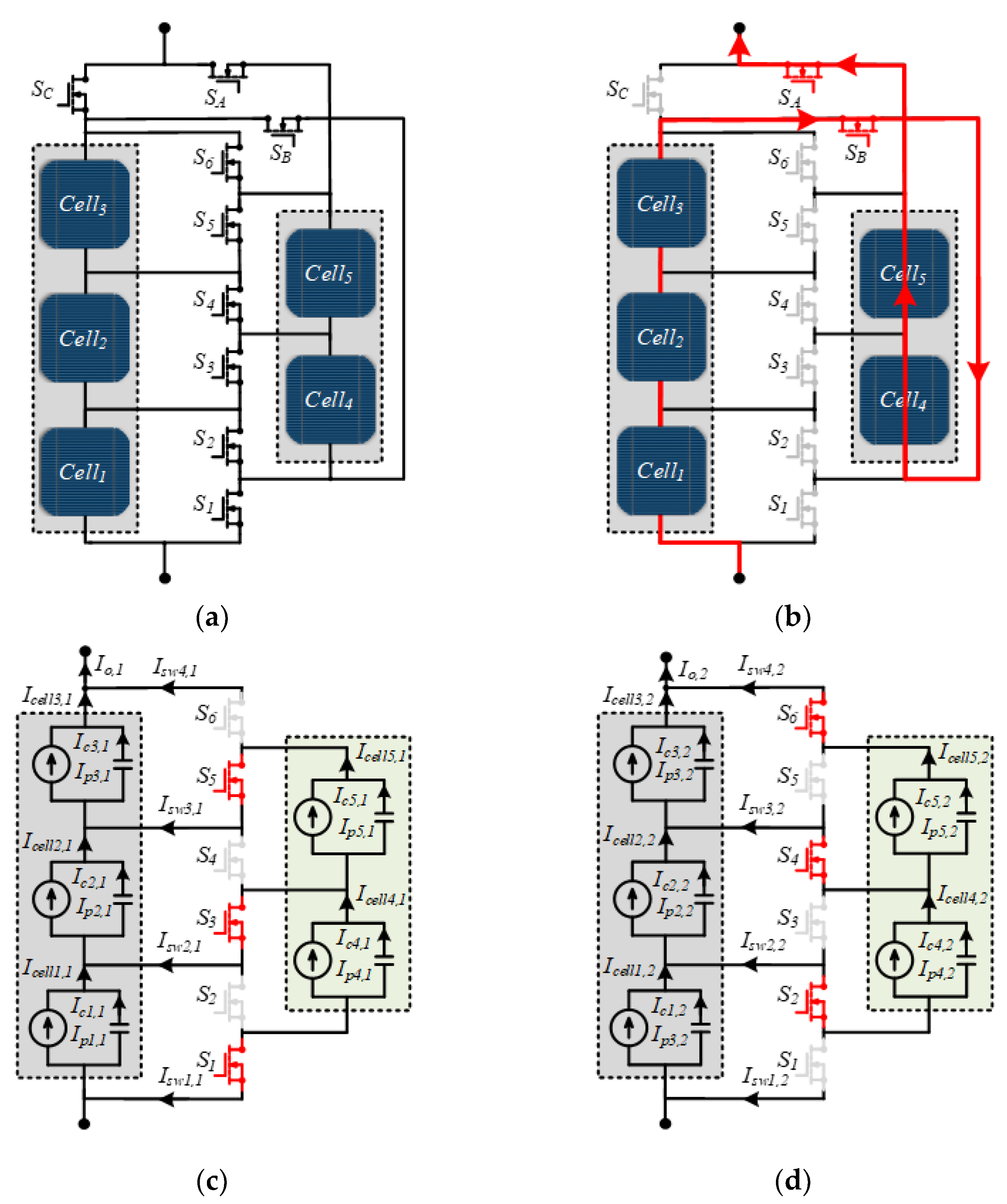
The introduced DPP-based architecture using diffusion capacitances of five PV cells is depicted in Figure 7. The ADCR DPP-based voltage equalizer is a combination of PV cells connected in series when there is no mismatch. However, the ADCR reconfigures itself to a capacitorless SC-based DPP voltage equalizer architecture under mismatch conditions [18]. For voltage equalization, diffusion capacitances of PV cells are used. Additionally, the introduced topology uses three extra switches to achieve reconfiguration in the DCR topology. Despite using three additional switches, the benefits of the introduced reconfiguration architecture are not impaired. Moreover, the traditional DCR topology is continuously switching at a high frequency even when there is no mismatch.
Furthermore, the high switching frequency operation of the proposed ADCR reconfiguration methodology under partial shading conditions is similar to the traditional DCR topology. However, the efficiency and performance of introduced architecture under normal conditions can dramatically improve in comparison to traditional DCR topology. Additionally, the introduced reconfigurable voltage equalizer also boosts the voltage by connected the available PV cells in series to achieve the desire application requirements. Furthermore, the introduced ADCR can be applied to the subpanel or panel level PV applications by using external capacitors. The extra passives and active components can easily be accommodated on the back of a PV panel junction box.

3.1. Mode of Operations

The introduced ADCR voltage equalizer has three modes of operation, which are shown in Figure 7. The introduced ADCR voltage equalizer operates in Mode 1 under no mismatch. During mismatch, the ADCR splits into two strings and starts to operate in Mode 2 and Mode 3. Hence, under mismatch, the string of N series-connected cells are connected parallel with a switched-ladder string of N-1 PV cells. This switched-ladder-based string is used for charge balancing during mismatch. The charge balancing is performed at a high switching frequency by switching repetition in Mode 2 and Mode 3 to acquire the desire PV cell voltage equalization.

3.1.1. Mode 1

Under no-mismatch conditions, the introduced ADCR voltage equalizer operates in Mode 1. The schematic of the ADCR voltage equalizer in Mode 1 is shown in Figure 7b. The equivalent circuit shows that all PV cells are in series, and the same current follows through all PV cells. In Mode 1, the switches SA and SB turned ON to bring the PV cells in series by keeping the switches S1, S2, S3, S4, S5, S6, and SC in OFF-state.

3.1.2. Mode 2

The equivalent circuit configuration for the introduced ADCR voltage equalizer in Mode 2 is presented in Figure 7c. In Mode 2, the switches S1, S3, S5, and SC are in ON-state by keeping all other switches S2, S4, S6, SA, and SB in OFF-state. In Figure 7c, each PV cell is equivalently illustrated as a combination of a light-generated current Ipi,1, and diffusion capacitance current Ici,1 (i = 1–5). In Mode 2, the diffusion capacitance gets charged to process the mismatched power and the current flows are depicted in Figure 7c. The current flow through the PV cells can be written as
I c e l l 3 , 2 = I c e l l 5 , 2 + I c e l l 2 , 2 = I c e l l 4 , 2 + I c e l l 1 , 2 = I o , 2
where Icell1,2, Icell2,2, Icell3,2, Icell4,2, and Icell5,2 are the cell1, cell2, cell3, cell4, and cell5 current during Mode 2, respectively. Similarly, Io,2 is the output currents during Mode 2.

3.1.3. Mode 3

In Mode 3, the switches S2, S4, S6, and SC are turned ON by turning all other switches S1, S3, S5, SA, and SB OFF. In this mode, the ADCR redistribute or discharges the mismatch charges stored during Mode 2. The equivalent circuit configuration is shown in Figure 7d, which is a combination of light generate current Ipi,3 and diffusion capacitance current Ici,3. Moreover, the current flow through the PV cells can be written as
I c e l l 3 , 3 + I c e l l 5 , 3 = I c e l l 2 , 3 + I c e l l 4 , 3 = I c e l l 1 , 3 = I o , 3
where Icell1,3, Icell2,3, Icell3,3, Icell4,3, and Icell5,3 are the cell1, cell2, cell3, cell4, and cell5 current during Mode 3, respectively. Similarly, Io,3 is the output current during Mode 3.

3.2. Power Loss Analysis

The major losses in the introduced reconfigurable ADCR architecture are due to MOSFET switches, which include switching and conduction losses. The ON-state power (Pon) and switching power losses (Pswloss) can be calculated by
P o n = I 2 R o n
P s w l o s s = 1 2 V D S [ i ( t s w _ o n ) × t o n + i ( t s w _ o f f ) × t o f f ] f s w
where Ron is the ON-state resistance of the MOSFETs and I is the current flowing through the switches while the switch is in ON-state. Similarly, VDS is the drain to source voltage of MOSFET, i(tsw_on) is the instantaneous MOSFET current during the turn-ON, i(tsw_off) is the current during the turn-OFF, ton and toff are the rise and fall time of the switch, which can be found from the datasheet.
The overall power losses for ADCR can be found from (8) and (9), which are given as
P t = { P o n ,   V d V t P o n + P s w l o s s ,   V d > V t
where Pt is the total power loss, Vd is the voltage difference between the maximum and minimum voltage of the PV cells, and Vt is the threshold voltage value.

3.3. Proposed Reconfiguration Method

The examination of the proposed work is performed by considering a system similar to a system shown in Figure 7. For the examination, five PV panels are considered, where each panel consists of twelve series-connected PV cells. The proposed reconfiguration algorithm is presented in Figure 8. In the proposed work, the voltage and irradiance across each PV panel are measured. Based on these measured values, the algorithm performed a reconfiguration. Firstly, the voltage differences are calculated. If the voltage differences exceed a certain defined threshold value, it indicates that there is a mismatch between the series-connected panels. Hence, the algorithm converts the series system into a DPP system. Afterward, the irradiances over the PV panels are measured to monitor the status of the system that the mismatch still exists or not. If the irradiance difference over the PV panels is less than a defined threshold, the algorithm brings the system back to a series-connected system. The algorithm is tested under various partial shadings cases in PSIM, as discussed in the following section.

4. Results and Discussion

To validate the significance of a proposed ADCR voltage equalizer, a simulation test was built in PSIM. The specifications of a PV panel consisting of twelve solar PV cells in series used for the validation are given in Table 1. The ADCR circuit used for the simulation test is depicted in Figure 7. For evaluation, several mismatch cases (i.e., Case 1, Case 2, Case 3, and Case 4) were developed by varying the irradiance (E) over the PV panels shown in Figure 7. The mismatch cases are given in Figure 9. The irradiances were varied from 1000 W/m2 to 250 W/m2. Hence, the output currents of the PV panels were distinct due to the different irradiances. These mismatch cases were developed by considering the applications, which are of variable shapes, e.g., solar cars, solar wearable bags, etc.
Moreover, the operating frequency (f) of the MOSFET switches during mismatch under Modes 2 and 3 is 100 kHz at a 50% duty cycle.
Furthermore, the inherent diffusion capacitance Cd of PV cells is 1 mF when considering the capacitor voltage ripples ∆Vd less than 5%. Therefore, a capacitance of 50 µF is considered by considering the capacitor voltage ripples ∆Vd for a PV panel in Table 1, which consists of twelve PV cells in series. Hence, the series connection of PV cells brings their capacitances in parallel. As mentioned above, the Cd depends on the biasing voltage, carrier lifetime, and cell area. In [48], the value of Cd at the MPP voltage (i.e., 0.574 V) is greater than 6.0 mF for a PV cell size of 125 mm × 125 mm. In other examples, the Cd is 100 μF at 0.43 V for a PV cell size 20 mm × 40 mm with a carrier lifetime of 4.12 × 10⁻⁵ s at 0.43 V [47] and around 20 µF for a PV cell size of 152 mm × 152 mm with a carrier lifetime of 6.5 × 10⁻⁷ s. Additionally, the Cd can also be calculated as [11]:
C d = 1 2 π f R s h
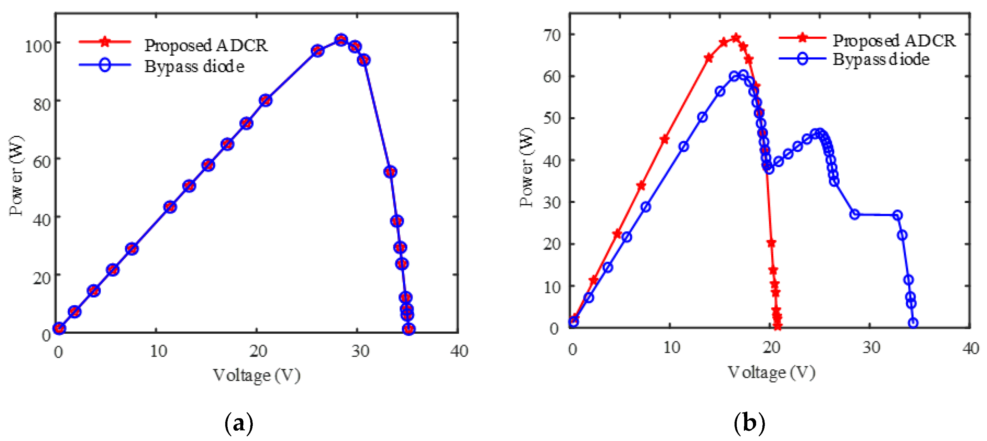
The output power–voltage (P-V) characteristic curves for the introduced ADCR voltage equalizer and traditional bypass diode architecture under various mismatch conditions are presented in Figure 10. For the bypass diode architecture, five PV panels are considered, which are connected in series and each panel has a parallel-connected bypass diode. The results in Figure 10 show that under mismatch conditions, the P-V characteristics remain convex with only one MPP for ADCR DPP topology.
However, there are several MPPs when using the bypass diode in Figure 10b–d for mismatch cases 2–4, respectively. Hence, the ADCR significantly minimizes the computational complexity of the MPPT scheme for MPP tracking.
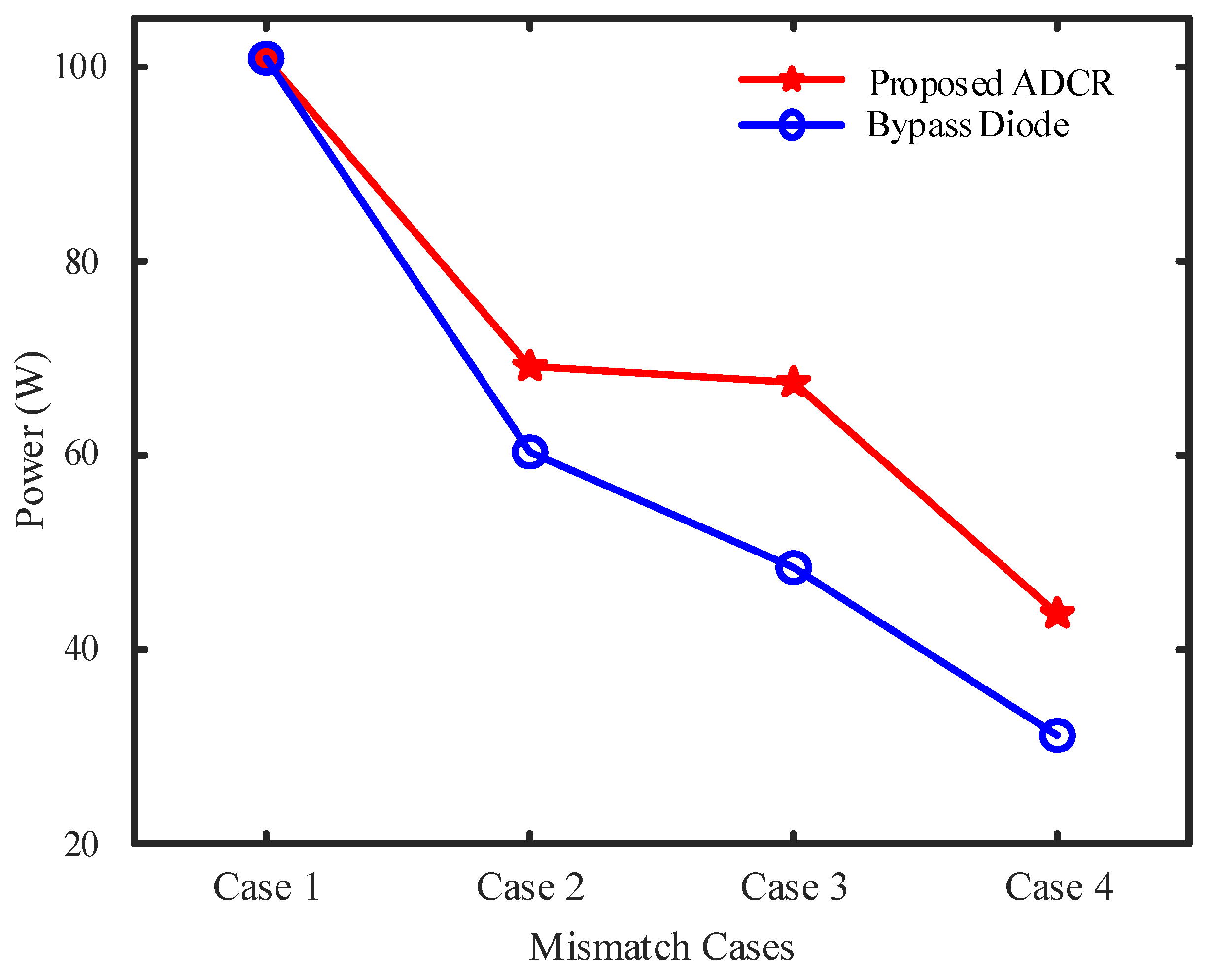
Furthermore, Figure 11 illustrates the maximum output power harvested by the introduced ADCR reconfigurable DPP and a conventional bypass diode topology under the mismatch cases shown in Figure 9. In Figure 11, the power harvested by the bypass diode architecture is 100.89 W, 60.34 W, 48.43 W, and 31.15 W for mismatch Case 1, Case 2, Case 3, and Case 4, respectively. However, it is 100.89 W, 69.15 W, 67.49 W, and 43.69 W for Case 1, Case 2, Case 3, and Case 4, respectively for the ADCR voltage equalizer. Hence, it shows that the bypass diode architecture loses a significant amount of power even under low mismatch scenarios. Moreover, the result in Figure 11 shows that the ADCR is 28% (Case 4) more efficient than traditional bypass diode architecture under severe mismatch conditions. Therefore, the introduced ADCR architecture causes a significant improvement in power extraction.
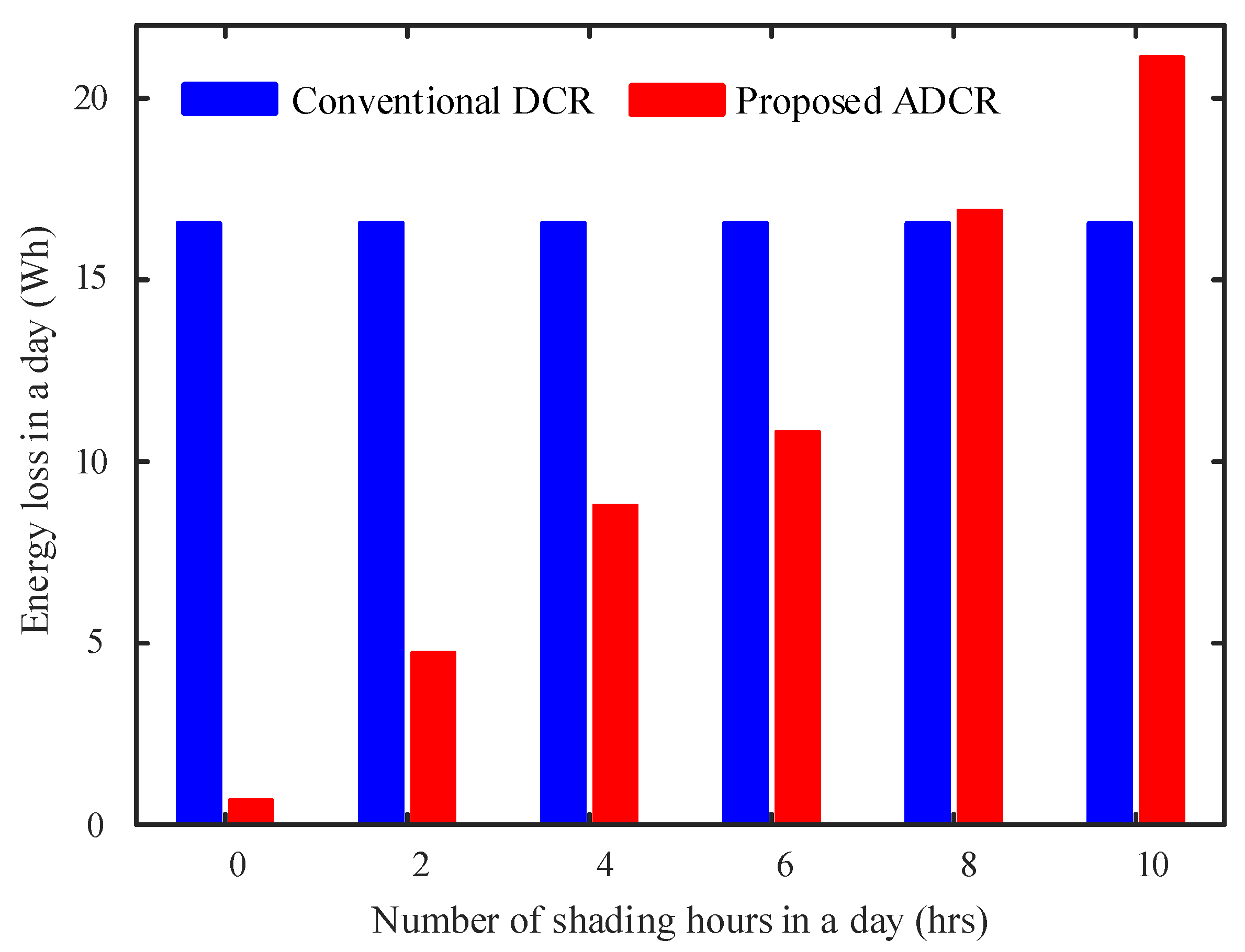
In Figure 12, the introduced reconfiguration architecture in Figure 9 is compared with the existing conventional DCR architecture in Figure 7a. The comparison is based on the energy loss in a day by considering the peak sun hours (PSH) to be equal to ten. For evaluation, a 1.180 kW system is considered consisting of 59 solar PV panels, where 30 series-connected panels are connected in parallel with a switched ladder-based string consisting of 29 series-connected PV panels, which are used for charge transfer. The rating of each solar PV panel is given in Table 1. The MOSFETs used for evaluation are IRF9910, which is switching at 100 kHz in DPP mode. Six different scenarios are considered, as shown in Figure 12, i.e., 0, 2, 4, 6, 8, and 10 h of shading in a day. The shading pattern is similar to mismatch Case 2 in Figure 9, where one panel from a string consisting of an N panel and the other from N-1 is shaded. It can be seen from Figure 12 when the shading is less than 8 hours in a day that the introduced ADCR lost less energy than the conventional DCR. However, if the system has a shading of 8 hours or more, the introduced ADCR lost more energy than the conventional approach. However, the introduced ADCR is more effective as compare to traditional DCR because the number of shading hours in a day is very less or even there is no shading throughout the day.
Additionally, the voltages across the PV panels using the introduced ADCR technique are given in Table 2 under the various mismatch cases shown in Figure 9. It can be seen from Table 2 that the PV panel voltages are identical even under conditions of severe mismatch. Hence, the voltage equalization helps in the disappearance of local MPPs, which not only improves the MPPT performance but also the reliability of the overall PV system.
The above discussion indicates the effect of mismatch in a string consisting of series-connected PV panels. It was observed that the mismatch in the PV string causes a substantial power reduction even when the PV panels encounter a small percentage of shading. Moreover, in a PV setup with an ADCR architecture, the energy yield under various mismatch conditions is at its maximum when compared to a PV array with bypass diodes and DCR DPP architecture. Additionally, the resulting P-V characteristics curve has only one power peak when ADCR is used. Hence, ADCR improves tracking efficiency by reducing the complexity of MPPT algorithms. In all, the PV panel array with ADCR strategy extracted noticeable higher energy under mismatch. Overall, the ADCR topology can be used for the PV cell, subpanel, and panel-level applications by carefully selecting the electrical components without affecting the performance and efficiency of the system.

5. Conclusions

This paper proposed a new cell/panel-level power electronics (PEs)-based active diffusion charge redistribution (ADCR) reconfigurable mismatch mitigation technique. The introduced technique detects the mismatch by measuring the PV cell/panel voltages and irradiance level across the solar PV cells/panels. The difference between the cell/panel voltages greater than the threshold voltage confirms the occurrence of mismatch. The proposed architecture increases the energy yield and improves the overall efficiency under the shade and no shade scenarios. This reconfiguration architecture brings the solar cells/panels under no mismatch in series and reconfigures itself into a voltage equalizer differential power processing (DPP) architecture during mismatch. Moreover, ADCR only processes partial power in order to minimize the number of external energy storage components. For this purpose, parallel-connected capacitances of PV cells/panels are used for power balancing at a cell/panel level. The results show that the ADCR string yields more energy under normal and various mismatched conditions compared to the traditional PV cells/panels connected in series with bypass diodes. The ADCR is also compared with conventional diffusion charge redistribution (DCR) architecture under different shading hours in a day. The ADCR lost less energy when compared with DCR. Furthermore, the ADCR boosts the voltage under no shade conditions. Additionally, the introduced ADCR is flexible, as it can be applied to cell/subpanel/panel-level PV applications by carefully considering the parallel-connected capacitors. The extra passive and active components can be placed on the rear side of a PV panel junction box.

Author Contributions

Conceptualization, K.A.K.N. and Y.Y.; methodology, K.A.K.N. and Y.Y.; software, K.A.K.N.; validation, K.A.K.N., Y.Y. and T.K. and D.S.; writing—original draft preparation, K.A.K.N.; writing—review and editing, K.A.K.N., Y.Y. and T.K. and D.S.; visualization, K.A.K.N., Y.Y., T.K. and D.S.; supervision, Y.Y., T.K. and D.S. All authors have read and agreed to the published version of the manuscript.

Funding

This research received no external funding.

Conflicts of Interest

The authors declare no conflict of interest.

References

  1. REN21. Renewable Energy Policy Network for the 21st Century Renewables 2017; Global Status Report—REN21; REN21: Paris, France, 2017; pp. 1–302. [Google Scholar]
  2. Fraunhofer ISE-Institut fur Solare Energiesysteme, 2021. In Recent Facts about Photovoltaics in Germany; Available online: https://www.ise.fraunhofer.de/ (accessed on 9 May 2021).
  3. Olalla, C.; Hasan, M.N.; Martínez-Salamero, L. Recoverable Energy in Photovoltaic Systems with Submodule Level Dispersion Losses. Sol. Energy 2020, 198, 376–384. [Google Scholar] [CrossRef]
  4. Silvestre, S.; Boronat, A.; Chouder, A. Study of Bypass Diodes Configuration on PV Modules. Appl. Energy 2009, 86, 1632–1640. [Google Scholar] [CrossRef]
  5. Niazi, K.A.K.; Yang, Y.; Khan, H.A.; Sera, D. Performance Benchmark of Bypassing Techniques for Photovoltaic Modules. In Proceedings of the 2019 IEEE Applied Power Electronics Conference and Exposition (APEC), Anaheim, CA, USA, 17–21 March 2019; pp. 3164–3168. [Google Scholar]
  6. Belhachat, F.; Larbes, C. A Review of Global Maximum Power Point Tracking Techniques of Photovoltaic System under Partial Shading Conditions. Renew. Sustain. Energy Rev. 2018, 92, 513–553. [Google Scholar] [CrossRef]
  7. Alonso-García, M.C.; Ruiz, J.M.; Chenlo, F. Experimental Study of Mismatch and Shading Effects in the I–V Characteristic of a Photovoltaic Module. Sol. Energy Mater. Sol. Cells 2005, 90, 329–340. [Google Scholar] [CrossRef]
  8. Kim, K.A.; Krein, P.T. Reexamination of Photovoltaic Hot Spotting to Show Inadequacy of the Bypass Diode. IEEE J. Photovolt. 2015, 5, 1435–1441. [Google Scholar] [CrossRef]
  9. Ahsan, S.; Niazi, K.A.K.; Khan, H.A.; Yang, Y. Hotspots and Performance Evaluation of Crystalline-Silicon and Thin-Film Photovoltaic Modules. Microelectron. Reliab. 2018, 88, 1014–1018. [Google Scholar] [CrossRef]
  10. Olalla, C.; Maksimovic, D.; Deline, C.; Martinez-Salamero, L. Impact of Distributed Power Electronics on the Lifetime and Reliability of PV Systems. Prog. Photovolt. Res. Appl. 2017, 25, 821–835. [Google Scholar] [CrossRef]
  11. Niazi, K.A.K.; Yang, Y.; Nasir, M.; Sera, D. Evaluation of Interconnection Configuration Schemes for PV Modules with Switched-Inductor Converters under Partial Shading Conditions. Energies 2019, 12, 2802. [Google Scholar] [CrossRef] [Green Version]
  12. Velasco-Quesada, G.; Guinjoan-Gispert, F.; Pique-Lopez, R.; Roman-Lumbreras, M.; Conesa-Roca, A. Electrical PV Array Reconfiguration Strategy for Energy Extraction Improvement in Grid-Connected PV Systems. IEEE Trans. Ind. Electron. 2009, 56, 4319–4331. [Google Scholar] [CrossRef] [Green Version]
  13. Sai Krishna, G.; Moger, T. Reconfiguration Strategies for Reducing Partial Shading Effects in Photovoltaic Arrays: State of the Art. Sol. Energy 2019, 182, 429–452. [Google Scholar] [CrossRef]
  14. Kaushika, N.D.; Gautam, N.K. Energy Yield Simulations of Interconnected Solar PV Arrays. IEEE Trans. Energy Convers. 2003, 18, 127–134. [Google Scholar] [CrossRef]
  15. Olalla, C.; Hasan, M.N.; Deline, C.; Maksimović, D. Mitigation of Hot-Spots in Photovoltaic Systems Using Distributed Power Electronics. Energies 2018, 11, 726. [Google Scholar] [CrossRef] [Green Version]
  16. Chu, G.; Wen, H.; Hu, Y.; Jiang, L.; Yang, Y.; Wang, Y. Low-Complexity Power-Balancing-Point Based Optimization for Photovoltaic Differential Power Processing. IEEE Trans. Power Electron. 2020, 10306–10322. [Google Scholar] [CrossRef]
  17. Kasper, M.; Bortis, D.; Kolar, J.W. Classification and Comparative Evaluation of PV Panel-Integrated DC–DC Converter Concepts. IEEE Trans. Power Electron. 2013, 29, 2511–2526. [Google Scholar] [CrossRef]
  18. Chang, A.H.; Avestruz, A.; Leeb, S.B. Capacitor-Less Photovoltaic Cell-Level Power Balancing Using Diffusion Charge Redistribution. IEEE Trans. Power Electron. 2014, 30, 537–546. [Google Scholar] [CrossRef]
  19. Jeon, Y.; Lee, H.; Kim, K.A.; Park, J. Least Power Point Tracking Method for Photovoltaic Differential Power Processing Systems. IEEE Trans. Power Electron. 2016, 32, 1941–1951. [Google Scholar] [CrossRef]
  20. Stauth, J.T.; Seeman, M.D.; Kesarwani, K. Resonant Switched-Capacitor Converters for Sub-Module Distributed Photovoltaic Power Management. IEEE Trans. Power Electron. 2012, 28, 1189–1198. [Google Scholar] [CrossRef]
  21. Kesarwani, K.; Stauth, J.T. A Comparative Theoretical Analysis of Distributed Ladder Converters for Sub-Module PV Energy Optimization. In Proceedings of the 2012 IEEE 13th Workshop on Control and Modeling for Power Electronics (COMPEL), Kyoto, Japan, 10–13 June 2012; pp. 1–6. [Google Scholar]
  22. Uno, M.; Kukita, A. PWM Switched Capacitor Converter with Switched-Capacitor-Inductor Cell for Adjustable High Step-Down Voltage Conversion. IEEE Trans. Power Electron. 2018, 34, 425–437. [Google Scholar] [CrossRef]
  23. Gokdag, M.; Akbaba, M.; Gulbudak, O. Switched-Capacitor Converter for PV Modules under Partial Shading and Mismatch Conditions. Sol. Energy 2018, 170, 723–731. [Google Scholar] [CrossRef]
  24. Bergveld, H.J.; Büthker, D.; Castello, C.; Doorn, T.; de Jong, A.; van Otten, R.; de Waal, K. Module-Level DC/DC Conversion for Photovoltaic Systems: The Delta-Conversion Concept. IEEE Trans. Power Electron. 2012, 28, 2005–2013. [Google Scholar] [CrossRef]
  25. Lavado Villa, L.F.; Ho, T.-P.; Crebier, J.-C.; Raison, B. A Power Electronics Equalizer Application for Partially Shaded Photovoltaic Modules. IEEE Trans. Ind. Electron. 2012, 60, 1179–1190. [Google Scholar] [CrossRef]
  26. Khan, O.; Xiao, W. Review and Qualitative Analysis of Submodule-Level Distributed Power Electronic Solutions in PV Power Systems. Renew. Sustain. Energy Rev. 2017, 76, 516–528. [Google Scholar] [CrossRef]
  27. Niazi, K.A.K.; Yang, Y.; Sera, D. Review of Mismatch Mitigation Techniques for PV Modules. IET Renew. Power Gener. 2019, 13, 2035–2050. [Google Scholar] [CrossRef]
  28. Ramli, M.Z.; Salam, Z. A Simple Energy Recovery Scheme to Harvest the Energy from Shaded Photovoltaic Modules during Partial Shading. IEEE Trans. Power Electron. 2014, 29, 6458–6471. [Google Scholar] [CrossRef]
  29. Shenoy, P.S.; Krein, P.T. Differential Power Processing for DC Systems. IEEE Trans. Power Electron. 2012, 28, 1795–1806. [Google Scholar] [CrossRef]
  30. Shimizu, T.; Hirakata, M.; Kamezawa, T.; Watanabe, H. Generation Control Circuit for Photovoltaic Modules. IEEE Trans. Power Electron. 2001, 16, 293–300. [Google Scholar] [CrossRef] [Green Version]
  31. Niazi, K.A.K.; Yang, Y.; Liu, W.; Sera, D. Sub-Module Level Differential Power Processing for Parallel-Connected Architecture in Photovoltaic Systems. In Proceedings of the 2019 21st European Conference on Power Electronics and Applications (EPE ’19 ECCE Europe), Marseille, France, 9 September–13 October 2019; pp. 1–9. [Google Scholar]
  32. Khan Niazi, K.A.; Yang, Y.; He, J.; Khan, A.Z.; Sera, D. Switched-Capacitor-Inductor-Based Differential Power Converter for Solar PV Modules. In Proceedings of the 2019 IEEE Energy Conversion Congress and Exposition (ECCE), Baltimore, MD, USA, 29 September–3 October 2019; pp. 4613–4618. [Google Scholar]
  33. Uno, M.; Kukita, A. Single-Switch Voltage Equalizer Using Multistacked Buck–Boost Converters for Partially Shaded Photovoltaic Modules. IEEE Trans. Power Electron. 2014, 30, 3091–3105. [Google Scholar] [CrossRef]
  34. Uno, M.; Kukita, A. Current Sensorless Equalization Strategy for a Single-Switch Voltage Equalizer Using Multistacked Buck–Boost Converters for Photovoltaic Modules under Partial Shading. IEEE Trans. Ind. Appl. 2016, 53, 420–429. [Google Scholar] [CrossRef]
  35. Uno, M.; Kukita, A. Single-Switch Single-Magnetic PWM Converter Integrating Voltage Equalizer for Partially Shaded Photovoltaic Modules in Standalone Applications. IEEE Trans. Power Electron. 2017, 33, 1259–1270. [Google Scholar] [CrossRef]
  36. Uno, M.; Kukita, A. PWM Converter Integrating Switched Capacitor Converter and Series-Resonant Voltage Multiplier as Equalizers for Photovoltaic Modules and Series-Connected Energy Storage Cells for Exploration Rovers. IEEE Trans. Power Electron. 2016, 32, 8500–8513. [Google Scholar] [CrossRef]
  37. Chu, G.; Wen, H.; Jiang, L.; Hu, Y.; Li, X. Bidirectional Flyback Based Isolated-Port Submodule Differential Power Processing Optimizer for Photovoltaic Applications. Sol. Energy 2017, 158, 929–940. [Google Scholar] [CrossRef] [Green Version]
  38. Peter, P.K.; Agarwal, V. Current Equalization in Photovoltaic Strings with Module Integrated Ground-Isolated Switched Capacitor DC–DC Converters. IEEE J. Photovolt. 2014, 4, 669–678. [Google Scholar] [CrossRef]
  39. Jeevandoss, C.R.; Kumaravel, M.; Kumar, V.J. A Novel Measurement Method to Determine the $C$$V$ Characteristic of a Solar Photovoltaic Cell. IEEE Trans. Instrum. Meas. 2010, 60, 1761–1767. [Google Scholar] [CrossRef]
  40. Kim, K.A.; Xu, C.; Jin, L.; Krein, P.T. A Dynamic Photovoltaic Model Incorporating Capacitive and Reverse-Bias Characteristics. IEEE J. Photovolt. 2013, 3, 1334–1341. [Google Scholar] [CrossRef]
  41. Friesen, G.; Ossenbrink, H.A. Capacitance Effects in High-Efficiency Cells. Sol. Energy Mater. Sol. Cells 1997, 48, 77–83. [Google Scholar] [CrossRef]
  42. Kumar, R.A.; Suresh, M.S.; Nagaraju, J. Silicon (BSFR) Solar Cell AC Parameters at Different Temperatures. Sol. Energy Mater. Sol. Cells 2005, 85, 397–406. [Google Scholar] [CrossRef]
  43. Zaraket, J.; Aillerie, M.; Salame, C. Capacitance Evolution of Photovoltaic Solar Modules under the Influence of Electrical Stress. Energy Procedia 2015, 74, 1466–1475. [Google Scholar] [CrossRef]
  44. Satpathy, P.R.; Sharma, R. Diffusion Charge Compensation Strategy for Power Balancing in Capacitor-Less Photovoltaic Modules during Partial Shading. Appl. Energy 2019, 255, 113826. [Google Scholar] [CrossRef]
  45. Jayakrishnan, R.; Gandhi, S.; Suratkar, P. Correlation between Solar Cell Efficiency and Minority Carrier Lifetime for Batch Processed Multicrystalline Si Wafers. Mater. Sci. Semicond. Process. 2011, 14, 223–228. [Google Scholar] [CrossRef]
  46. Sharma, S.K.; Pavithra, D.; Sivakumar, G.; Srinivasamurthy, N.; Agrawal, B.L. Determination of Solar Cell Diffusion Capacitance and Its Dependence on Temperature and 1 MeV Electron Fluence Level. Sol. Energy Mater. Sol. Cells 1992, 26, 169–179. [Google Scholar] [CrossRef]
  47. Anil Kumar, R.; Suresh, M.S.; Nagaraju, J. Measurement and Comparison of AC Parameters of Silicon (BSR and BSFR) and Gallium Arsenide (GaAs/Ge) Solar Cells Used in Space Applications. Sol. Energy Mater. Sol. Cells 2000, 60, 155–166. [Google Scholar] [CrossRef]
  48. Uno, M.; Saito, Y.; Urabe, S.; Yamamoto, M. PWM Switched Capacitor-Based Cell-Level Power Balancing Converter Utilizing Diffusion Capacitance of Photovoltaic Cells. IEEE Trans. Power Electron. 2019, 34, 10675–10687. [Google Scholar] [CrossRef]
Figure 1. Global estimated energy share of renewable sources from 2019 [1].
Electronics 10 01121 g001
Figure 2. Series-connected photovoltaic (PV) cells (cell1, cell2, and cell3): (a) no mismatch or partial shading; (b) under mismatch with bypass diode D in ON-state; (c) power–voltage (P-V) characteristics under mismatch and no mismatch. Here, Im is PV cell current and Ib is the bypass current passing through the bypass diode.
Electronics 10 01121 g002
Figure 3. Infrared (IR) thermographic images of PV panels under partial shading showing hotspots: (a) shading from the panel in the front row, (b) un-expected shading on a bottom left cell, and (c) shading caused whole PV sub-module bypassed.
Electronics 10 01121 g003
Figure 4. Distributed power electronic (DPE) converters.
Electronics 10 01121 g004
Figure 5. (a) Diffusion charge redistribution (DCR) DPP architecture; (b) power–voltage (P-V) characteristics during mismatch and without mismatch using [17].
Electronics 10 01121 g005
Figure 6. A photovoltaic (PV) solar cell model: (a) without diffusion capacitance; (b) with diffusion capacitance. Here, Cd is the diffusion capacitance, D is the anti-parallel diode, Rs is the series resistance, and Rsh is the shunt resistance.
Electronics 10 01121 g006
Figure 7. A photovoltaic (PV) system with five series-connected PV cells: (a) general schematic; (b) Mode 1; (c) Mode 2; (d) Mode 3.
Electronics 10 01121 g007
Figure 8. Flow chart for the proposed reconfiguration.
Electronics 10 01121 g008
Figure 9. Mismatch cases with different irradiances over the PV cells.
Electronics 10 01121 g009
Figure 10. Power–voltage (P-V) characteristic curves for the active diffusion charge redistribution (ADCR) reconfigurable architecture and traditional bypass diode technique with series connection of five PV panels under the mismatch cases shown in Figure 9: (a) Case 1; (b) Case 2; (c) Case 3; (d) Case 4.
Electronics 10 01121 g010aElectronics 10 01121 g010b
Figure 11. Power extraction under mismatch cases in Figure 9 for a PV setup using the introduced ADCR in Figure 7 and traditional bypass diode architectures.
Electronics 10 01121 g011
Figure 12. Energy loss in a day under mismatch Case 2 in Figure 9 for a conventional DCR in Figure 5a and the introduced ADCR architectures in Figure 7.
Electronics 10 01121 g012
Table 1. PV panel rating at standard temperature condition (STC): Irradiance (E) = 1000 W/m2 and Temperature (T) = 25°.
Maximum power (Pmax)20.18 W
Voltage at maximum power (Vmp)5.68 V
Current at maximum power(Imp)3.55 A
Voltage at open-circuit (Voc)7.03 V
Current at short-circuit (Isc)3.80 A
Table 2. PV panel voltages under mismatch cases given in Figure 9 for the introduced ADCR DPP voltage equalizer architecture.
CasesVc1 (V)Vc2 (V) Vc3 (V)Vc4 (V)Vc5 (V)
Case 15.685.685.685.685.68
Case 26.366.746.676.365.74
Case 36.656.586.406.656.58
Case 46.126.276.216.276.21
Publisher’s Note: MDPI stays neutral with regard to jurisdictional claims in published maps and institutional affiliations.