Article

A Dual Source Switched-Capacitor Multilevel Inverter with Reduced Device Count

1
Department of Electrical Engineering, ZHCET, Aligarh Muslim University, Aligarh 202002, India
2
Department of Electrical, Electronic and Computer Engineering, University of Western Australia, Crawley, WA 6009, Australia
3
Industrial Engineering Department, College of Engineering, King Saud University, P.O. Box 800, Riyadh 11421, Saudi Arabia
4
Electrical Engineering Department, College of Engineering, King Saud University, P.O. Box 800, Riyadh 11421, Saudi Arabia
*
Authors to whom correspondence should be addressed.
Electronics 2022, 11(1), 67; https://doi.org/10.3390/electronics11010067
Submission received: 15 November 2021 / Revised: 22 December 2021 / Accepted: 24 December 2021 / Published: 26 December 2021

Abstract

:
Implementing voltage boost multilevel inverter topologies for PV and fuel cell energy sources is highly advantageous. Switched-capacitor multilevel inverters (SCMLI) have a step-up feature with low device requirements and can remove the need for high gain dc-dc converters leading to reduced overall system bulk. This work proposes a dual input SCMLI to achieve an output of nineteen levels while using a low number of components and high boosting factor and self-balancing of capacitor voltages. A comprehensive analysis of the proposed structure is presented, focusing on component requirements, cost and dynamic performance. The efficiency and loss distribution during operation is also provided. The operation and real-time performance of the SCMLI have been verified by simulation. Experimental results further validate the simulation results.

1. Introduction

As the installation of renewable energy systems is gaining traction across the globe, the significance of multilevel inverters (MLIs) as dc-ac conversion devices is at its zenith [1,2]. Since many renewable power sources are composed of numerous low-voltage dc sources such as solar photovoltaic cells, ultra-capacitors, or battery storage systems, they are ideal for forming multiple connected dc-links. A similar case can be observed in hydrogen-based fuel cells investigated for use in high specific energy applications like onboard power systems [3]. MLIs can generate high efficiency and power quality dc-ac conversion at high voltage and high power levels. The reduced harmonic content, reduced individual device ratings and the filter size are some of the attributes of MLIs. Traditionally, MLIs were devised as cascaded H-bridge, flying capacitor and neutral point clamped configurations. Flying capacitor and neutral point clamped topologies have substantial capacitor counts with higher levels, leading to cost and reliability issues and capacitor voltage balancing requirements [4]. Since their inception, numerous evolved configurations have been developed to eliminate their setbacks. Furthermore, the later developed topologies outperform the three traditional topologies in component counts. Currently, researchers are developing MLIs with an application-based approach with fault-tolerance, modularity, efficiency and even weight and volume requirements in mind [5,6,7].
Extensive efforts have been made in the design of reduced device count structures [8,9,10]. On a similar note, fault-tolerant reduced device count topologies [10,11] and device count optimization [12] have also been investigated by researchers. Nevertheless, the need for a high number of dc sources leads to practical realization and control complexity issues, especially with renewable power sources with fluctuating voltage magnitudes. Initially, the inclusion of capacitors in MLIs can be observed in the two classical configurations, NPC and FC themselves. Recently, SCMLI-based topologies, including combinations of capacitors and switch modules in series/parallel configuration, have gained researchers’ attention, particularly for applications where a voltage boosting feature is advantageous [13,14,15,16,17]. Low magnitude voltage, including PV or fuel cell, can be significantly increased as a result of this boosting feature. This warrants the exclusion of boost dc/dc converters, which would otherwise be required as intermediate devices [18], thus significantly reducing the overall generation system size, efficiency, and complexity. Nevertheless, the challenges of the inflated device count with higher levels are currently being addressed.
Interestingly, the replacement of multiple dc sources of a CHB with capacitors is investigated in [19], thus requiring a single dc source. The structure proposed in [20] can generate a total of nine levels using two capacitors, one dc source and nine switches with a two-fold boosting factor. The self-balancing of capacitor voltages has the benefit of eliminating the need for additional instrumentation or control circuitry. Similarly, a topology using three interconnected H-bridge structures, one dc source and two capacitors can produce seven levels with a boosting factor of three [21]. The fault-tolerant operation of an SCMLI topology is also investigated in [22]. Feedback linearization control for voltage and current ripple reduction under dynamic and steady operating conditions includes ANN (artificial neural network) in [23].
Furthermore, to reduce the switch current ratings and enable a larger power capability, the usage of multiple dc sources that can split the overall load current among multiple conduction paths is suitable. A 55-level topology with three asymmetrical dc sources and seven capacitors is proposed in [24], but the large number of components involved can negatively affect its reliability. Seven-level modified PUC active rectifier based on floating weighting factors and ANN-MPC based on Lyapunov stability were presented in [24]. A topology using two asymmetrical dc sources, four capacitors and ten switches is presented in [16] with a specific method for capacitor charge balancing. More examples of multiple dc source topologies with reduced device count and self-balancing capabilities can be observed as in [25,26,27,28,29,30,31,32,33,34,35,36,37,38,39,40,41].
A new SCMLI topology has been proposed. The SCMLI is able to produce higher levels with a low device count. In Section 2, the SCMLI operation has been discussed. Comparative assessment of the topology is carried out in Section 3. The performance of the topology is verified in Section 4. The structure’s power loss analysis is carried out in Section 5. The conclusion of this work is presented in Section 6.

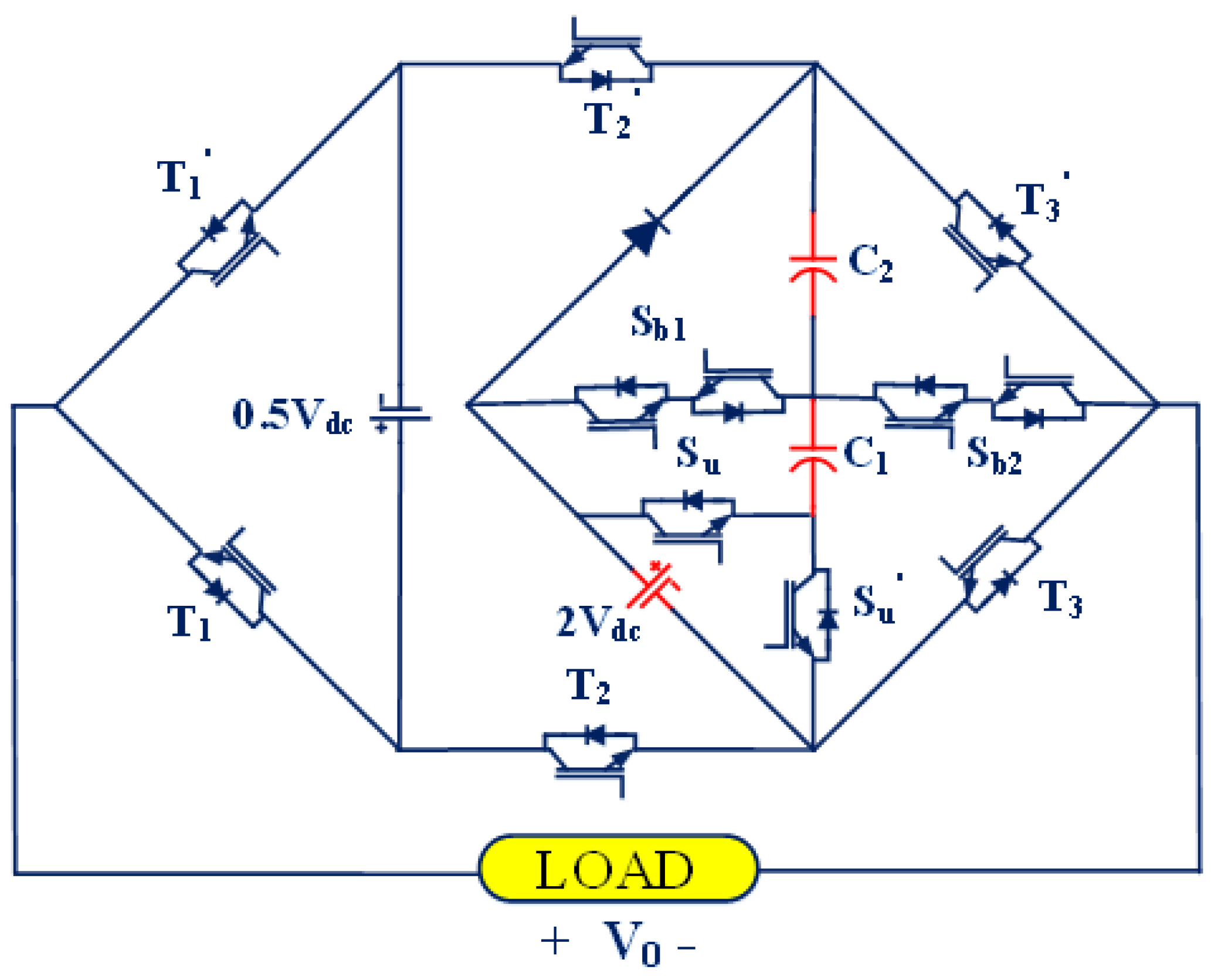
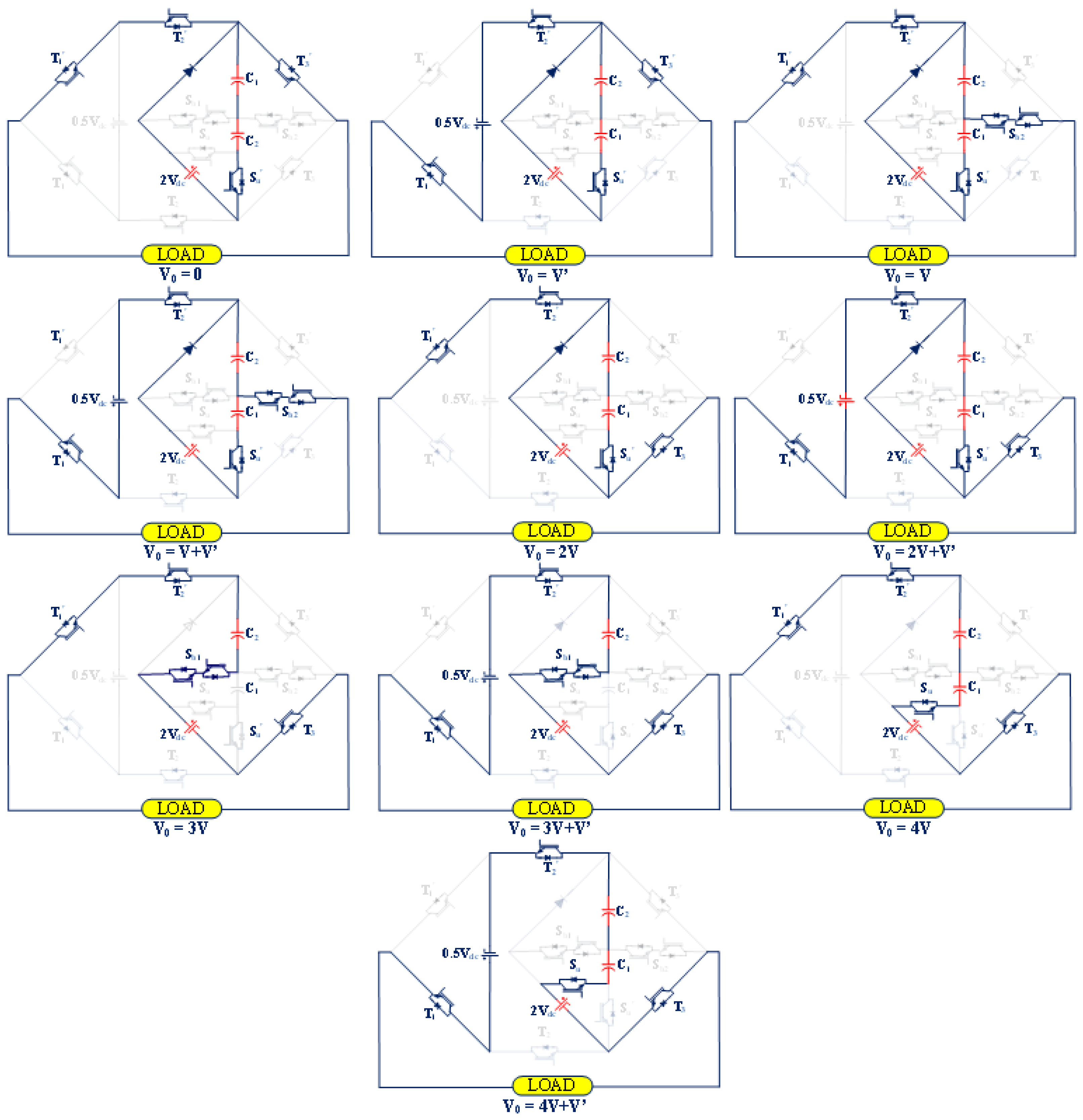
2. Proposed Topology

The schematic of the proposed topology is shown in Figure 1. The structure consists of two dc voltage sources, one power diode and ten switches, with two switches being bidirectional modules. The two dc sources possess per-unit values of 0.5Vdc and 2Vdc (a ratio of 4:1). The two capacitors, C1 and C2, create the boosting effect in their operation. They are charged in series with the 2Vdc source. The proposed topology can generate a total of 19 levels. The switching states are shown in Table 1. The ratio of the capacitors is C1/C2 = 0.5. The ratio between the total source voltage and peak output level, known as the boosting factor, is 4.5/2.5 = 1.8. The capacitor voltages are self-balanced through charging loops on certain levels. Figure 2 illustrates the various conduction paths in operation. The peak blocking voltages across various switches are as follows.
V ST 1 = V ST 1   = 0.5 V dc
V ST 2 = V ST 2   = 4.5 V dc
V Su = V Su   = 2 V dc
V Sb 1 = V dc
V Sb 2 = 3 V dc
V ST 3 = V ST 3   = 4 V dc
The TSV (total standing voltage) is computed as the summation of these voltages. The bidirectional switches require two modules with the same rating.
TSV = n = 1 10 Vsn = 30 V dc
The per-unit TSV of the structure is given as:
TSV p . u . = TSV V o , peak = 30 V dc 4.5 V dc = 6.66
The modulation scheme is either low frequency-based (LS-PWM) or high-frequency carrier-based (CB-PWM). Modulation at low frequencies possesses the advantage of reduced switching losses, dv/dt ratings and snubber losses. Low frequency-based modulation techniques comprise the nearest level control (NLC) and the selective harmonic elimination (SHE) methods. The SHE approach is optimum for reducing the filter size but involves the solution of complex non-linear transcendental equations, therefore, being computationally more intensive. Additionally, NLC is more convenient for closed-loop controlled systems. NLC-PWM has been used in this work. The visual representation of NLC-PWM is depicted in Figure 3. The modulation index Ma is given as:
θ i = M a sin 1 ( 2 i 1 N 1 )
Knowing the modulation index Ma, number of levels N and switch index i, the calculation for switching angle θi [36,37] is given as:
M a   =   V r e f V 0  

3. Comparative Assessment

The proposed SCMLI is compared with recently devised works with a similar level count. The basis for comparisons includes the quantity of power semiconductor switches, diodes, capacitors, gate drivers, boosting factor and cost function. The comparison is shown in Table 2. The proposed SCMLI is superior in terms of component count per unit level, particularly considering levels produced as compared to previous works. Additionally, the comparison is also made using the metric of the cost function (CF) as defined in [38]. An intelligent compact multilevel converter based on passivity ANFIS control was presented in [31].
C F = ( N s w + N g d + N d + N C + α × T S V p u )   N d c
N C F = C F N L  
From Table 2, it is seen that the proposed SCMLI has the lowest NCF for two values of α. This verifies that the proposed converter has a high number of levels with lower component requirements and a cost-effective design.

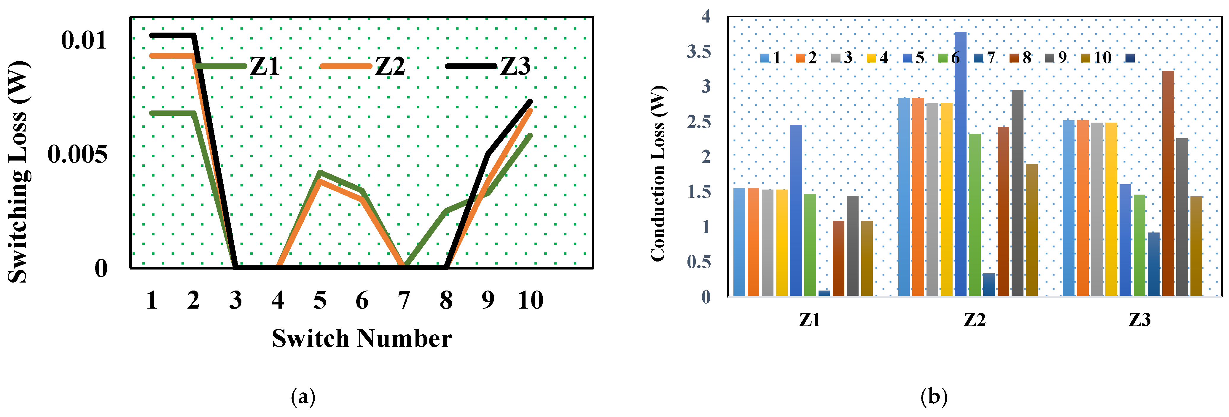
4. Power Loss Analysis

The proposed converter’s thermal loss model was developed to estimate the topology’s loss distribution across various components and efficiencies. The non-ideality in semiconductor components leads to conduction (PC) and switching losses (PS). In other words, power dissipation across ON-state resistance leads to conduction losses, and non-instantaneous transitions between ON and OFF states lead to switching losses. The total conduction loss in IGBTs and diodes is obtained using:
P   c s w = V s w i ( t ) + R s i β ( t )
P   c D = V D i ( t ) + R D i 2 ( t ) ,
P c   = k = 1 N s w 1 2 π 0 2 π ( V s w i ( t ) + R s i β ( t ) ) d t + k = 1 N D 1 2 π 0 2 π ( V D i ( t ) + R D i 2 ( t ) ) d t
where Vsw is the ON-state voltage drop across the switch and VD is the ON-state drop across the power diode. RS is the ON-state resistance of the switch, and RD stands for the ON-state resistance of the diode. Following an assumption of non-linear transitions between device current and voltages, the switching loss is for NS switches, and with f switching frequency is evaluated as:
P s   = [ k = 1 N s (   N O N k E O N k + N O F F k E O F F k )   ] × f ,
with N O N k , N O F F k , E O N k , and E O F F k being associated with switch number (k), are the number of transitions and energy losses in turning ON and OFF, respectively. The total thermal is:
P loss   = P c + P s  
Conversion efficiency is given by:
η = P 0 P 0 + P loss   × 100 %
The PLECS platform was utilized for the thermal analysis of the SCMLI. The module IGW40N60H3, PG6DI capacitor is implemented with a peak voltage of 450 V. Figure 4 shows the conversion efficiency as compared to two previous topologies. The corresponding distribution of losses for loads is shown in Figure 5. As evident, the conduction losses are dominant due to low-frequency NLC PWM.

5. Results and Discussion

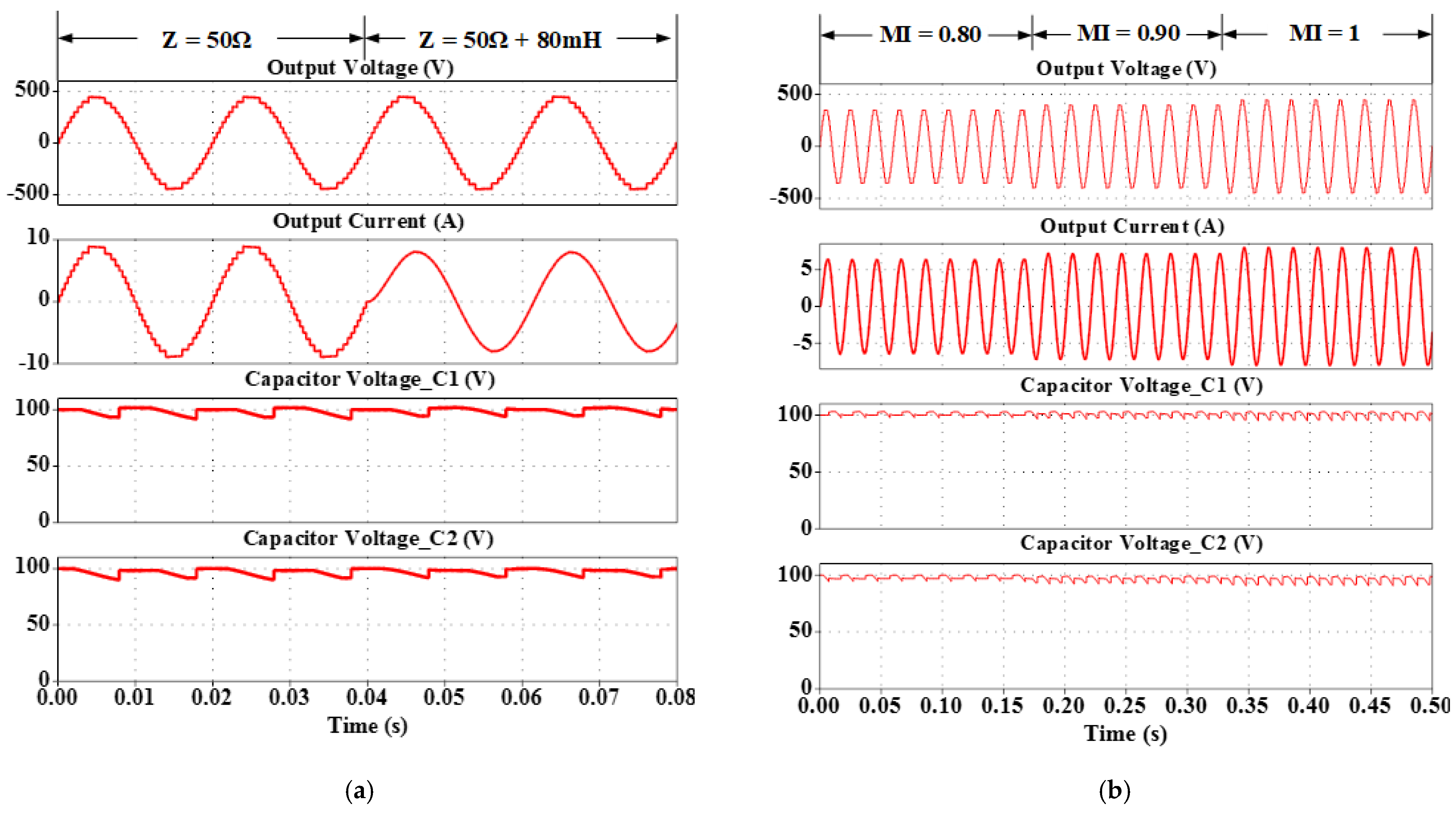
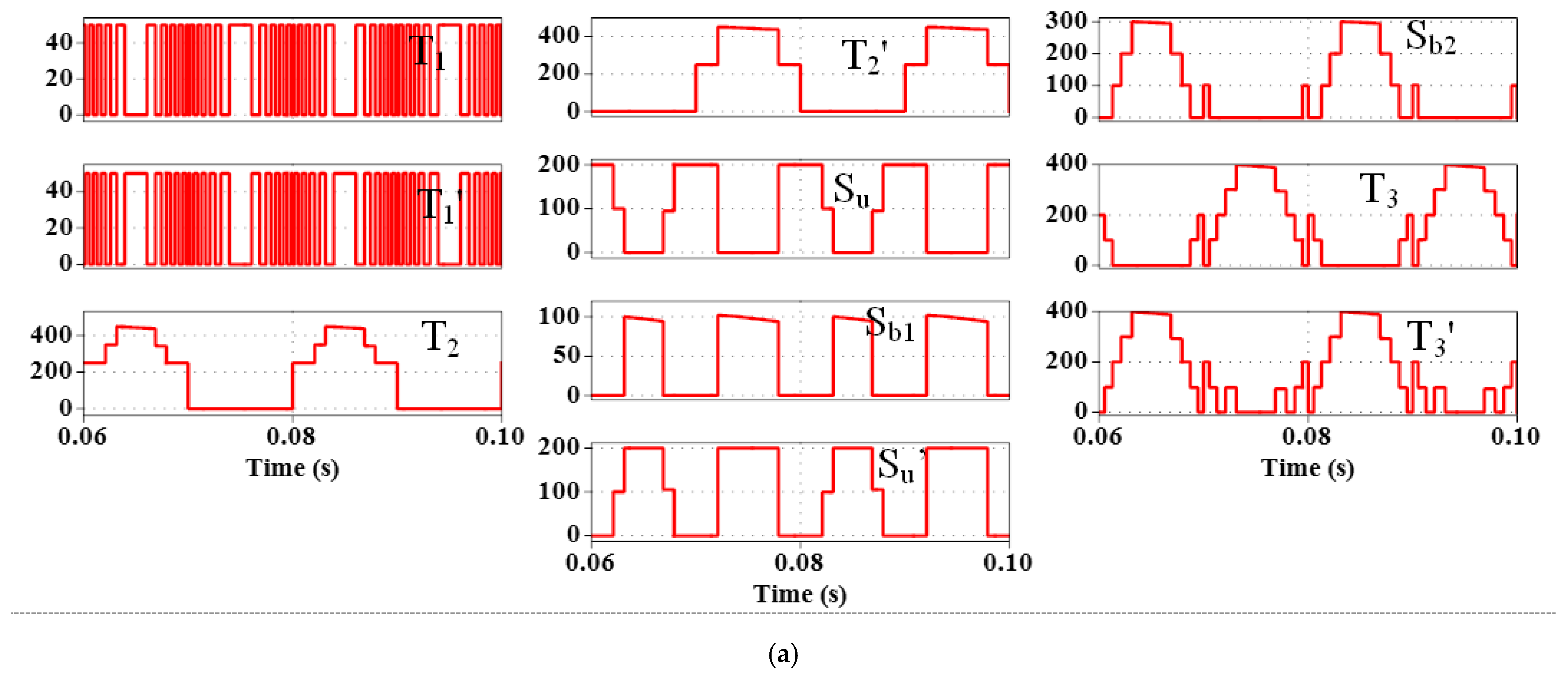
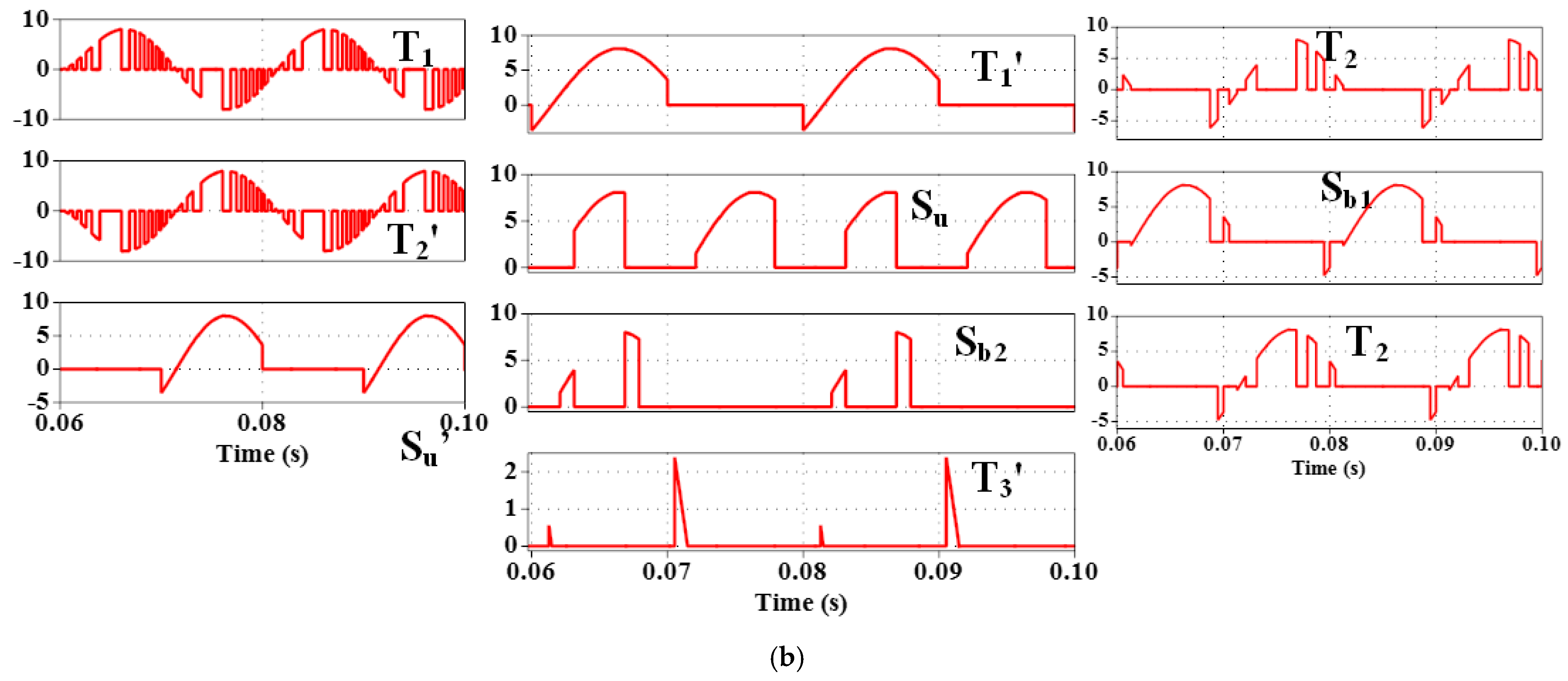
5.1. Simulation Results

The proposed SCMLI topology is simulated in MATLAB and PLECS environments. NLCPWM staircase modulation was used for generating a 19-level output with a 450 V peak at MI = 1.0 and 50 Hz frequency. The topology’s dynamic performance with load change was verified, and the load voltage, current and capacitor voltage waveforms are illustrated in Figure 6a. The load was changed from 50 Ω to 50 Ω + 40 mH at t = 0.04 s. Similarly, the output of the inverter with a varying modulation index of MI = 0.8, 0.9 and 1 can be observed in Figure 6b. Notably, the balance in capacitor voltages is maintained irrespective of alteration in load or MI. Furthermore, the voltage and current stresses of the switches with a load of 50 Ω + 40 mH are given in Figure 7a,b.

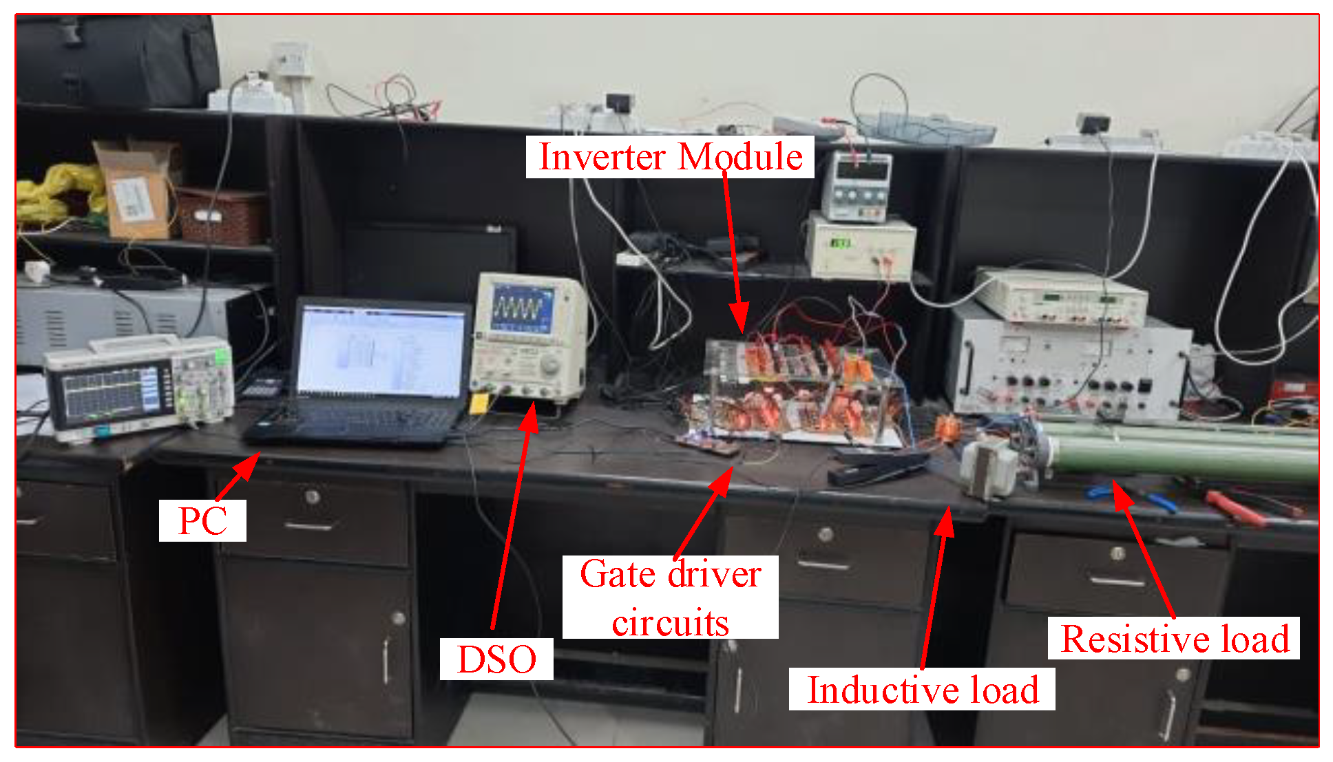
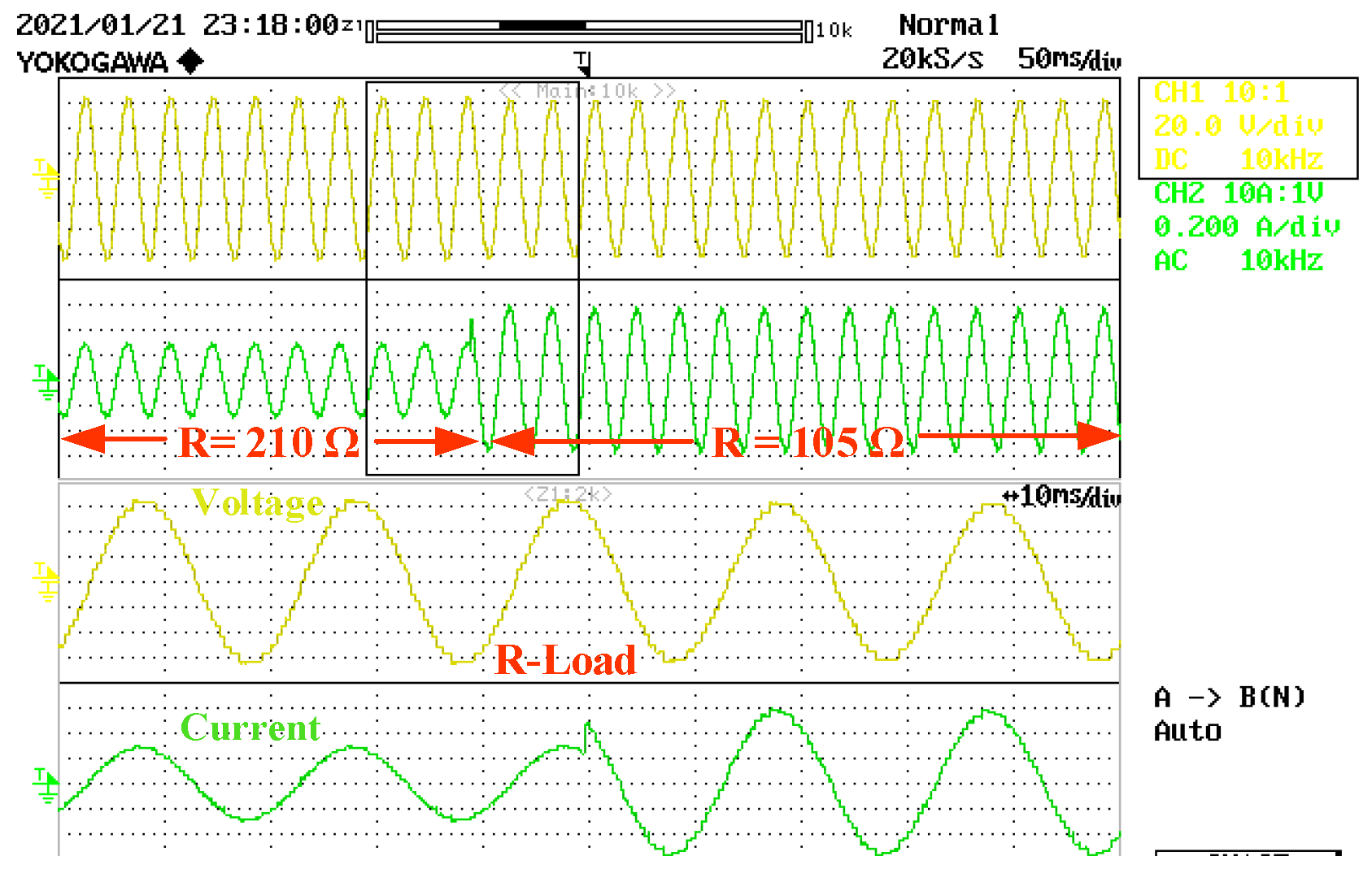
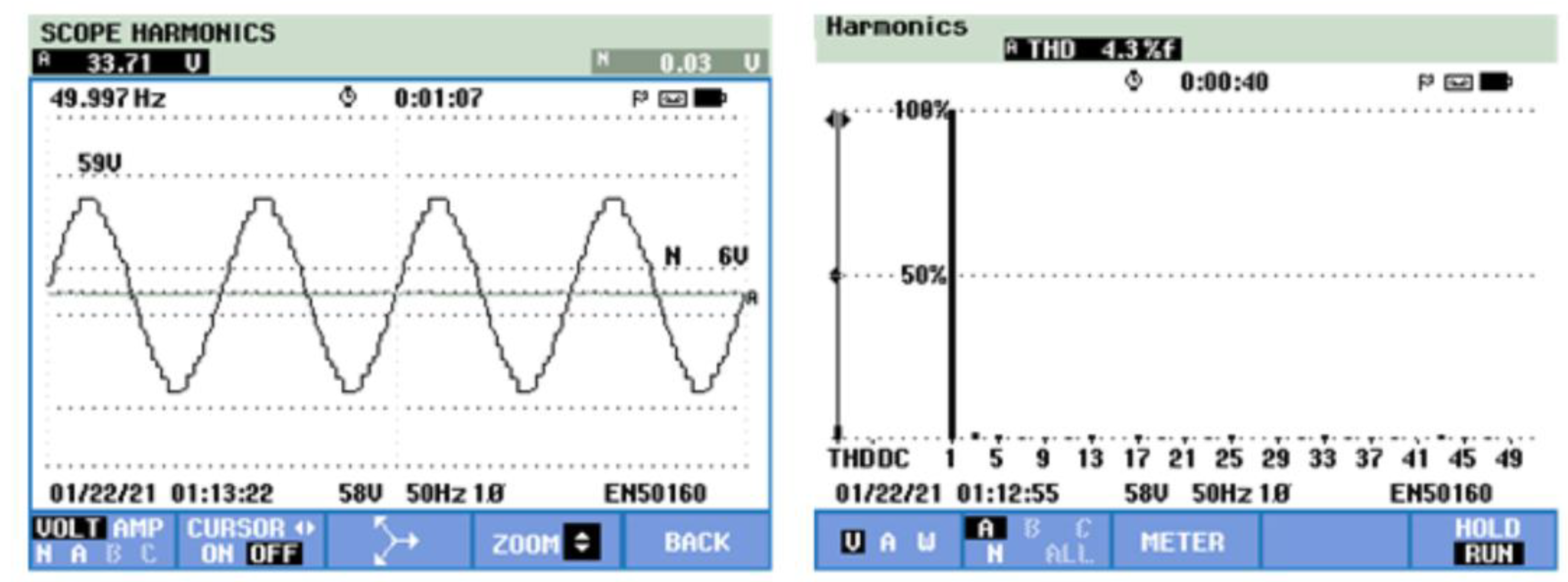
5.2. Experimental Verification

The laboratory prototype of the SCMLI topology is shown in Figure 8. The IGBT (IGW40N60H3) and PG6DI capacitors were used. TMS320F28335 DSP and TLP250H gate drivers were used for gating pulse control. A Yokogawa DL1640 oscilloscope was used to capture the resulting waveforms. A peak voltage of 63V at MI = 1 was created. Figure 9 depicts the 19-level load voltage waveform and current through a 210 Ω load. The voltage and current waveforms are in phase with similar wave shapes. The peak voltage and current values are 63 V and 0.3, respectively. Observably, the current lags the output voltage due to the inductive phase lag and is approaching a closer sinusoidal shape. To demonstrate the performance in dynamic conditions, R-load changes are also analyzed. The R-load changed from 210 Ω to 105 Ω, as shown in Figure 10. Additionally, waveforms during no-load to R-load transition are given in Figure 11. The harmonic profile of the 19-level waveform can be seen in Figure 12. The waveform has a THD of 4.3%, which meets EN50160 power quality standards and can eliminate filter demand due to minimal lower order harmonic content. The above results demonstrate the performance of the topology under varying operational requirements.

6. Conclusions

A multisource step-up multilevel inverter with low component requirements and high power quality has been discussed. The operation of the proposed SCMLI is demonstrated, and the self-balancing property of capacitor voltages is shown. Analysis of previous works in developing various MLIs and switched-capacitor configurations with their advantages and setbacks is presented. A comparison of the proposed SCMLI with recent topologies was conducted. The topology’s thermal loss analysis was carried out to show its thermal behavior and efficiency. Simulation results have been presented. Experimental results validate the performance in varied operating conditions (load and MI changes).

Author Contributions

Conceptualization, M.F. (Mohammad Fahad), M.T. and A.S.; formal analysis, M.F. (Mohammad Fahad), M.T., M.F. (Mohammad Faizan), A.A., A.S., H.D.T., S.A. and A.S.N.M.; funding acquisition, M.F. (Mohammad Fahad) and S.A.; investigation, M.F. (Mohammad Fahad), M.T., M.F. (Mohammad Faizan), A.A., A.S., H.D.T., S.A. and A.S.N.M.; methodology, M.F. (Mohammad Fahad), M.T., M.F. (Mohammad Faizan), A.A., A.S., H.D.T. and A.S.N.M.; supervision, M.T. and A.S.; writing—original draft, M.F. (Mohammad Fahad) and M.T.; writing—review and editing, M.F. (Mohammad Faizan), A.A., A.S., H.D.T., S.A. and A.S.N.M. All authors have read and agreed to the published version of the manuscript.

Funding

The authors extend their appreciation to King Saud University for funding this work through Researchers Supporting Project number (RSP-2021/387), King Saud University, Riyadh, Saudi Arabia.

Acknowledgments

The authors extend their appreciation to King Saud University for funding this work through Researchers Supporting Project number (RSP-2021/387), King Saud University, Riyadh, Saudi Arabia.

Conflicts of Interest

The authors declare no conflict of interest.

References

  1. Bhukya, M.N.; Kota, V.R.; Depuru, S.R. A Simple, Efficient, and Novel Standalone Photovoltaic Inverter Configuration with Reduced Harmonic Distortion. IEEE Access 2019, 7, 43831–43845. [Google Scholar] [CrossRef]
  2. Dhanamjayulu, C.; Khasim, S.R.; Padmanaban, S.; Arunkumar, G.; Holm-Nielsen, J.B.; Blaabjerg, F. Design and Implementation of Multilevel Inverters for Fuel Cell Energy Conversion System. IEEE Access 2020, 8, 183690–183707. [Google Scholar] [CrossRef]
  3. Chen, J.; Song, Q.; Yin, S.; Chen, J. On the Decentralized Energy Management Strategy for the All-Electric APU of Future More Electric Aircraft Composed of Multiple Fuel Cells and Supercapacitors. IEEE Trans. Ind. Electron. 2020, 67, 6183–6194. [Google Scholar] [CrossRef]
  4. Celanovic, N.; Boroyevich, D. A comprehensive study of neutral-point voltage balancing problem in three-level neutral-point-clamped voltage source PWM inverters. IEEE Trans. Power Electron. 2000, 15, 242–249. [Google Scholar] [CrossRef]
  5. Cao, W.; Mecrow, B.C.; Atkinson, G.J.; Bennett, J.W.; Atkinson, D.J. Overview of electric motor technologies used for more electric aircraft (MEA). IEEE Trans. Ind. Electron. 2012, 59, 3523–3531. [Google Scholar]
  6. Pradeep Kumar, V.V.S.; Fernandes, B.G. A Fault-Tolerant Single-Phase Grid-Connected Inverter Topology with Enhanced Reliability for Solar PV Applications. IEEE J. Emerg. Sel. Top. Power Electron. 2017, 5, 1254–1262. [Google Scholar] [CrossRef]
  7. Sarwar, M.I.; Sarwar, A.; Farooqui, S.A.; Tariq, M.; Fahad, M.; Beig, A.R.; Alamri, B. A Hybrid Nearest Level Combined with PWM Control Strategy: Analysis and Implementation on Cascaded H-Bridge Multilevel Inverter and its Fault Tolerant Topology. IEEE Access 2021, 9, 44266–44282. [Google Scholar] [CrossRef]
  8. Rodríguez, J.; Bernet, S.; Wu, B.; Pontt, J.O.; Kouro, S. Multilevel voltage-source-converter topologies for industrial medium-voltage drives. IEEE Trans. Ind. Electron. 2007, 54, 2930–2945. [Google Scholar] [CrossRef]
  9. Omer, P.; Kumar, J.; Surjan, B.S. A Review on Reduced Switch Count Multilevel Inverter Topologies. IEEE Access 2020, 8, 22281–22302. [Google Scholar] [CrossRef]
  10. Dewangan, N.K.; Gupta, S.; Gupta, K.K. Approach to synthesis of fault tolerant reduced device count multilevel inverters (FT RDC MLIs). IET Power Electron. 2019, 12, 476–482. [Google Scholar] [CrossRef]
  11. Kumar, D.; Nema, R.K.; Gupta, S. Investigation of Fault-Tolerant Capabilities of Some Recent Multilevel Inverter Topologies. Int. J. Electron. 2020, 108, 1957–1976. [Google Scholar] [CrossRef]
  12. Siddique, M.D.; Mekhilef, S.; Shah, N.M.; Memon, M.A. Optimal Design of a New Cascaded Multilevel Inverter Topology with Reduced Switch Count. IEEE Access 2019, 7, 24498–24510. [Google Scholar] [CrossRef]
  13. Chappa, A.; Gupta, S.; Sahu, L.K.; Gautam, S.P.; Gupta, K.K. Symmetrical and Asymmetrical Reduced Device Multilevel Inverter Topology. IEEE J. Emerg. Sel. Top. Power Electron. 2019, 9, 885–896. [Google Scholar] [CrossRef]
  14. Samizadeh, M.; Yang, X.; Karami, B.; Chen, W.; Blaabjerg, F.; Kamranian, M. A new topology of switched-capacitor multilevel inverter with eliminating leakage current. IEEE Access 2020, 8, 76951–76965. [Google Scholar] [CrossRef]
  15. Khan, M.N.H.; Forouzesh, M.; Siwakoti, Y.P.; Li, L.; Blaabjerg, F. Switched Capacitor Integrated (2n + 1)-Level Step-Up Single-Phase Inverter. IEEE Trans. Power Electron. 2020, 35, 8248–8260. [Google Scholar] [CrossRef]
  16. Taheri, A.; Rasulkhani, A.; Ren, H.P. An Asymmetric Switched Capacitor Multilevel Inverter with Component Reduction. IEEE Access 2019, 7, 127166–127176. [Google Scholar] [CrossRef]
  17. Jagabar Sathik, M.; Sandeep, N.; Almakhles, D.; Blaabjerg, F. Cross Connected Compact Switched-Capacitor Multilevel Inverter (C3-SCMLI) Topology with Reduced Switch Count. IEEE Trans. Circuits Syst. II Express Briefs 2020, 67, 3287–3291. [Google Scholar] [CrossRef]
  18. Ahmad, J.; Pervez, I.; Sarwar, A.; Tariq, M.; Fahad, M.; Chakrabortty, R.K.; Ryan, M.J. Performance Analysis and Hardware-In-the-Loop (HIL) Validation of Single Switch High Voltage Gain DC-DC Converters for MPP Tracking in Solar PV System. IEEE Access 2020, 9, 48811–48830. [Google Scholar] [CrossRef]
  19. Khoun Jahan, H.; Abapour, M.; Zare, K. Switched-Capacitor-Based Single-Source Cascaded H-Bridge Multilevel Inverter Featuring Boosting Ability. IEEE Trans. Power Electron. 2019, 34, 1113–1124. [Google Scholar] [CrossRef]
  20. Siddique, M.D.; Mekhilef, S.; Shah, N.M.; Sandeep, N.; Ali, J.S.M.; Iqbal, A.; Ahmed, M.; Ghoneim, S.S.M.; Al-Harthi, M.M.; Alamri, B.; et al. A Single DC Source Nine-Level Switched-Capacitor Boost Inverter Topology with Reduced Switch Count. IEEE Access 2020, 8, 5840–5851. [Google Scholar] [CrossRef]
  21. Lee, S.S. A Single-Phase Single-Source 7-Level Inverter with Triple Voltage Boosting Gain. IEEE Access 2018, 6, 30005–30011. [Google Scholar] [CrossRef]
  22. Bikdeli, E.; Adabi, J.; Rezanejad, M.; Gholamian, S.A. Investigation on Fault Tolerant Capability of a Single Source Switched Capacitor Multilevel Inverter. IEEE Trans. Ind. Electron. 2020, 68, 7921–7930. [Google Scholar] [CrossRef]
  23. Mehrasa, M.; Babaie, M.; Sharifzadeh, M.; Al-Haddad, K. An Input-Output Feedback Linearization Control Method Synthesized by Artificial Neural Network for Grid-Tied Packed E-Cell Inverter. IEEE Trans. Ind. Appl. 2021, 57, 3131–3142. [Google Scholar] [CrossRef]
  24. Taghvaie, A.; Adabi, J.; Rezanejad, M. A Multilevel Inverter Structure Based on a Combination of Switched-Capacitors and DC Sources. IEEE Trans. Ind. Inform. 2017, 13, 2162–2171. [Google Scholar] [CrossRef]
  25. Babaie, M.; Mehrasa, M.; Sharifzadeh, M.; Al-Haddad, K. Floating Weighting Factors ANN-MPC Based on Lyapunov Stability for Seven-Level Modified PUC Active Rectifier. IEEE Trans. Ind. Electron. 2022, 69, 387–398. [Google Scholar] [CrossRef]
  26. Rawa, M.; Siddique, M.D.; Mekhilef, S.; Shah, N.M.; Bassi, H.; Seyedmahmoudian, M.; Horan, B.; Stojcevski, A. Dual input switched-capacitor-based single-phase hybrid boost multilevel inverter topology with reduced number of components. IET Power Electron. 2020, 13, 881–891. [Google Scholar] [CrossRef]
  27. Samadaei, E.; Kaviani, M.; Bertilsson, K. A 13-levels module (K-Type) with two DC sources for multilevel inverters. IEEE Trans. Ind. Electron. 2019, 66, 5186–5196. [Google Scholar] [CrossRef]
  28. Siddique, M.D.; Mekhilef, S.; Sarwar, A.; Alam, A.; Mohamed Shah, N. Dual asymmetrical dc voltage source based switched capacitor boost multilevel inverter topology. IET Power Electron. 2020, 13, 1481–1486. [Google Scholar] [CrossRef]
  29. Alishah, R.S.; Hosseini, S.H.; Babaei, E.; Sabahi, M.; Zare, A. Extended high step-up structure for multilevel converter. IET Power Electron. 2016, 9, 1894–1902. [Google Scholar] [CrossRef]
  30. Zamiri, E.; Vosoughi, N.; Hosseini, S.H.; Barzegarkhoo, R.; Sabahi, M. A New Cascaded Switched-Capacitor Multilevel Inverter Based on Improved Series-Parallel Conversion with Less Number of Components. IEEE Trans. Ind. Electron. 2016, 63, 3582–3594. [Google Scholar] [CrossRef]
  31. Lee, S.S.; Lee, K.B.; Alsofyani, I.M.; Bak, Y.; Wong, J.F. Improved Switched-Capacitor Integrated Multilevel Inverter with a DC Source String. IEEE Trans. Ind. Appl. 2019, 55, 7368–7376. [Google Scholar] [CrossRef]
  32. Barzegarkhoo, R.; Moradzadeh, M.; Zamiri, E.; Madadi Kojabadi, H.; Blaabjerg, F. A New Boost Switched-Capacitor Multilevel Converter with Reduced Circuit Devices. IEEE Trans. Power Electron. 2018, 33, 6738–6754. [Google Scholar] [CrossRef]
  33. Barzegarkhoo, R.; Zamiri, E.; Moradzadeh, M.; Shadabi, H. Symmetric hybridised design for a novel step-up 19-level inverter. IET Power Electron. 2017, 10, 1377–1391. [Google Scholar] [CrossRef]
  34. Roy, T.; Sadhu, P.K. A Step-Up Multilevel Inverter Topology Using Novel Switched Capacitor Converters with Reduced Components. IEEE Trans. Ind. Electron. 2021, 68, 236–247. [Google Scholar] [CrossRef]
  35. Talooki, M.F.; Rezanejad, M.; Khosravi, R.; Samadaei, E. A Novel High Step-Up Switched-Capacitor Multilevel Inverter with Self-Voltage Balancing. IEEE Trans. Power Electron. 2021, 36, 4352–4359. [Google Scholar] [CrossRef]
  36. Nguyen, M.H.; Kwak, S. Nearest-Level Control Method with Improved Output Quality for Modular Multilevel Converters. IEEE Access 2020, 8, 110237–110250. [Google Scholar] [CrossRef]
  37. Hu, P.; Jiang, D. A level-increased nearest level modulation method for modular multilevel converters. IEEE Trans. Power Electron. 2015, 30, 1836–1842. [Google Scholar] [CrossRef]
  38. Deliri, S.; Varesi, K.; Siwakoti, Y.P.; Blaabjerg, F. A boost type switched-capacitor multi-level inverter for renewable energy sources with Self-Voltage balancing of capacitors. Int. J. Energy Res. 2021, 45, 15217–15230. [Google Scholar] [CrossRef]
  39. Mehrasa, M.; Babaie, M.; Zafari, A.; Al-Haddad, K. Passivity ANFIS-Based Control for an Intelligent Compact Multilevel Converter. IEEE Trans. Ind. Inform. 2021, 17, 5141–5151. [Google Scholar] [CrossRef]
  40. Karimi, M.; Kargar, P.; Varesi, K.; Sanjeevikumar, P. Power quality improvement by a double-source multilevel inverter with reduced device and standing voltage on switches. In Power Quality in Modern Power Systems; Academic Press: Cambridge, MA, USA, 2021; pp. 245–282. [Google Scholar]
  41. Deliri, S.; Varesi, K.; Siwakoti, Y.P.; Blaabjerg, F. Generalized diamond-type single DC-source switched-capacitor based multilevel inverter with step-up and natural voltage balancing capabilities. IET Power Electron. 2021, 14, 1208–1218. [Google Scholar] [CrossRef]
Figure 1. Structure of proposed multilevel inverter topology.
Electronics 11 00067 g001
Figure 2. All positive conduction states.
Electronics 11 00067 g002
Figure 3. Nearest level modulation.
Electronics 11 00067 g003
Figure 4. Efficiency curve.
Electronics 11 00067 g004
Figure 5. Loss distribution across switches (a) Switching Loss (b) Conduction Loss.
Electronics 11 00067 g005
Figure 6. (a) Simulation results with load change (b) Simulation results with modulation index change.
Electronics 11 00067 g006
Figure 7. Switch stresses during simulation (a) Voltage Stress (b) Current Stress.
Electronics 11 00067 g007aElectronics 11 00067 g007b
Figure 8. Experimental Prototype.
Electronics 11 00067 g008
Figure 9. 19-level output waveform.
Electronics 11 00067 g009
Figure 10. Load change from 210 Ω to 105 Ω.
Electronics 11 00067 g010
Figure 11. Load change from no-load to 210 Ω.
Electronics 11 00067 g011
Figure 12. Harmonic spectrum.
Electronics 11 00067 g012
Table 1. Switching states.
T1T1T2T2SuSb1SuSb2T3T3VoC1C2
0101001001zeroCC
10010010010.5 VdcCC
0101001100VdcCC
10010011001.5 VdcCC
01010010102 VdcCC
10010010102.5 VdcCC
01010100103 Vdc-D
10010100103.5 Vdc-D
01011000104 VdcDD
10011000104.5 VdcDD
1010001010zeroCC
0110001010−0.5 VdcCC
1010001100−VdcCC
0110001100−1.5 VdcCC
1010001001−2 VdcCC
0110001001−2.5 VdcCC
1010100100−3 VdcD
0110100100−3.5 VdcD
1010100001−4 VdcDD
0110100001−4.5 VdcDD
Table 2. Comparative Assessment.
TopologyNLNdcNswNgdNdNcTSVpuVGCF
[24]1121111014.41.674.66
[26]1321411025.3324.56
[27]1721010225.523.14
[28]1721010225.523.14
[29]1321110116.31.54.18
[30]132181502525.76
[31]172181424624.82
[32]1921212645.82.253.85
Proposed1921210126.661.83.02
Publisher’s Note: MDPI stays neutral with regard to jurisdictional claims in published maps and institutional affiliations.

