Abstract
Power curtailment methods contribute to the frequency stability of power systems with a high share of photovoltaic generation. This paper focuses on an online strategy that estimates the output characteristic of a photovoltaic generator while operating in power curtailment mode by using voltage and current measurements and the nonlinear least-squares curve-fitting. In contrast to previously reported methods, this work introduces an improvement consisting of the estimation of the power losses of the electronic converter that connects the photovoltaic panel with the grid. Thus, the impact of a mismatch between the dc-side and the ac-side is reduced. The procedure is tested at different power levels and with fluctuations of irradiance and temperature. The results show that the converter efficiency, expressed as an exponential function with two quadratic equations, is associated with irradiance and temperature. It is also found that the two-stage converter efficiency is mainly affected by the irradiance level when the photovoltaic system operates on the left side of the power-voltage characteristic. In contrast, the temperature level influences the converter efficiency significantly when working on the right side of the maximum power point. The estimated efficiency curves can improve the accuracy of the power curtailment method and can be used for designing the two-stage converter. The effectiveness of the proposed power curtailment method has been tested in a two-stage photovoltaic system through MATLAB/Simulink.
1. Introduction
Photovoltaic (PV) power is becoming increasingly important in power systems due to the pollution-free power generation, the maturity of manufacturing technologies, and the low cost of operation [,]. However, the uncertainty of generated power in PV systems, caused by variations of weather conditions, produces some issues in the AC grid, such as frequency fluctuation [,]. In addition, the displacement of synchronous generators by renewable ones involves the deterioration of some ancillary services such as frequency control [,]. Therefore, the higher penetration of renewable energy in power systems and the lower responsiveness capacity in case of generation-demand mismatches, that appear during the regular operation of this kind of systems, affect the guarantee and the quality of the power supply [,]. Hence, the challenge is to increase the penetration of renewable energy in power systems in a way that security and efficiency are not compromised. To achieve this goal, apart from producing the necessary amount of energy to meet the demand, renewable generators must participate in the provision of ancillary services, understood as those fundamental activities to guarantee the safe operation and reliability of power systems. In the literature, it is possible to find many scientific contributions that address the topic of providing ancillary services by renewable generators, among which photovoltaic and wind generators stand out [,]. In particular, photovoltaic technology presents several characteristics that make it an ideal candidate to provide ancillary services to power systems: it is fully interconnected through power electronics, enabling it to provide a fast time response, it doesn’t possess any rotating mass that increments the time response, and it requires fewer maintenance hours in contrast to other renewable generators [].
Up to now, a variety of methods have been proposed for PV systems to solve these problems, which can be categorized into two main types: employing energy storage systems and introducing power curtailment methods []. The advantages of the latter approach are: the more straightforward implementation and the lower initial investment. There also exist numerous investigations on PV power curtailment methods.
In reference [], curve-fitting with voltage and current measurements is used to estimate the P-V characteristic and the Maximum Power Point (MPP). The two-stage inverter is regulated by a ripple control algorithm for implementing the curtailment requirement. Operating points can only be situated on the right side of the MPP, which may cause instability problems when step changes occur on irradiance. However, working on the right side achieves higher efficiency.
In reference [], a PV string in a PV array is operated as an auxiliary string to implement the Maximum Power Point Tracking (MPPT) algorithm for obtaining the available power. Other PV strings cooperate in carrying out Constant Power Generation (CPG) to achieve the AC power requirement. The main problems of this method are that the shading levels among strings may be different, and the communication between them may increase the complexity of its operation.
In reference [], the desired power is determined from the offline calculations using PV module datasheet values. The method enables fast frequency response and highly accurate performance, but additional sensors are needed for exact temperature and irradiance measurements.
In reference [], two current-voltage points are used to estimate the open-circuit current. Then, according to the empirical expression, the MPP can be calculated to implement the power curtailment method. This method is easier to implement, but it is highly affected by noise.
Among these, reference [] proposes a PV power curtailment algorithm that allows the PV system to be operated on both sides of the power-voltage curve. This method applies nonlinear least-squares curve-fitting to online voltage and current measurements to estimate the actual I-V curve, the P-V characteristic, and the MPP. The PV voltage control regulates pulse-width modulation (PWM) for controlling the DC/DC converter to satisfy the grid power requirement. Moreover, after analyzing the performance of the PV system, an effective method is proposed to solve unstable operation problems in case of sudden changes in the incoming irradiance and temperature.
All of the above mentioned methods estimate the maximum available power point and/or the entire P-V curve. However, none of them consider the power losses that occur in electronic converters. This is a fundamental issue, as a PV array is commonly equipped with a DC/DC converter and a DC/AC inverter: the former is used to implement the maximum power point tracking (MPPT) algorithm [,] and the latter serves to inject the electric energy into the AC grid. Power losses of components in those converters/inverters cause a mismatch between the actual AC power and the PV one. Thus, power losses cannot be ignored when a PV system is operated on the curtailed mode. This paper proposes a novel PV power curtailment strategy that takes into account the power losses in the electronic devices through their efficiency curve, calculated by nonlinear least-squares curve-fitting with variations of temperature and irradiance. The accuracy of the actual efficiency curve compared with test points is verified, and a control scenario with the power curtailment method is programmed in simulation.
Table 1 compares the characteristics of the existing power curtailment methods and the proposed one. Evidently, the proposed methodology is the first one to introduce the efficiency of the electronic converters in the curtailed operation calculations.

Table 1.
Existing and proposed methods for estimating the maximum available power point while operating suboptimally.
This paper is structured as follows: Section 2 introduces the single diode model, PV systems, and different PV power curtailment methods. Section 3 presents the arrangement of the grid-connected PV system under study, the strategy of PV power curtailment method proposed in [] with two-stage converter losses and the control scenario. Section 4 presents simulation results to verify the effectiveness of the proposed method. In Section 5, conclusions and prospects concerning the future research of this work are presented.
2. Overview of Photovoltaic Power Systems
This section introduces the single diode model (SDM), different configurations of photovoltaic systems, and PV power curtailment methods. The SDM is the most commonly used model in simulation because it offers a reasonable trade-off between simplicity and accuracy. The characteristics and explicit equations for the SDM are discussed in detail in the following subsection.
2.1. Single Diode Model
Figure 1 shows the equivalent circuit of the SDM consisting of a photovoltaic current source, a diode, and resistances [,]. The electrical behavior of a PV module is illustrated by its voltage-current (V-I) curve with the photovoltaic current and the Shockley diode equation.
where k, q, T, and n are the Boltzmann constant, the electron charge, the module temperature expressed in Kelvin, and the diode ideality factor, respectively. and represent the photovoltaic output voltage and current, respectively. is the photovoltaic current, is the saturation current, is the series resistance and represents the shunt resistance. Finally, and are the numbers of solar cells connected in parallel and series, respectively.
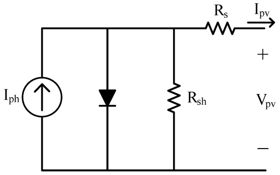
Figure 1.
Equivalent circuit of single diode model.
The parameters and are affected by irradiance and temperature. According to De Soto et al. [], and and their dependencies on irradiance and temperature can be expressed as:
where and are the short-circuit current and the nominal saturation current at reference temperature (298.15 K) and reference irradiance (1000 W/m), respectively. is the short-circuit temperature coefficient and is the energy bandgap of the concrete semiconductor being used in the PV cell.
The relationship between and can also be expressed as (5) by using the Lambert W function [,] with the parameters , , , and n, which are determined by environmental conditions.
The I-V curve can be obtained by using (5). Figure 2 shows the I-V characteristic of a solar array and the accuracy of explicit Equation (5) compared with the electrical Simulink data. Figure 2a are static characteristics when a specific solar array encounters different irradiance levels (600, 1000 and 1400 W/m). Figure 2b illustrates the I-V curves at different ambient temperatures (25, 50 and 75 °C) with the same irradiance 1000 W/m. As it can be seen in Figure 2, variations of irradiance affect the short-circuit current of a solar panel significantly, while the open-circuit voltage mainly depends on the temperature level. It also can be observed in Figure 2 that Equation (5) can represent the I-V curve almost perfectly.

Figure 2.
I-V characteristic calculated by explicit equation and Simulink: (a) Static characteristics with variations of irradiance, and (b) static characteristics with variations of temperature.
2.2. Photovoltaic Power Systems
In general, power systems with PV panels can be divided into three types, standalone PV systems, grid-connected PV systems, and hybrid PV systems []. Figure 3a shows the configuration of a stand-alone PV power system consisting of a PV array, two DC/DC converters, a DC/AC inverter, and an energy storage system. The energy storage system supplies the power to the load when the sunlight is insufficient and is charged when the generated power is higher than the load requirement. Figure 3b illustrates the diagram of a grid-connected power system, which can be subdivided into two systems, decentralized grid-connected PV systems, and central grid-connected PV systems. PV array is connected with DC/DC converters and a DC/AC inverter to fulfill the grid power requirement and execute the MPPT algorithm and the power curtailment method. Energy storage systems can also be attached to the grid-connected power system as a backup power supply. Figure 3c depicts a hybrid PV power system. Additional generators are connected to the AC grid for satisfying the grid power demand.
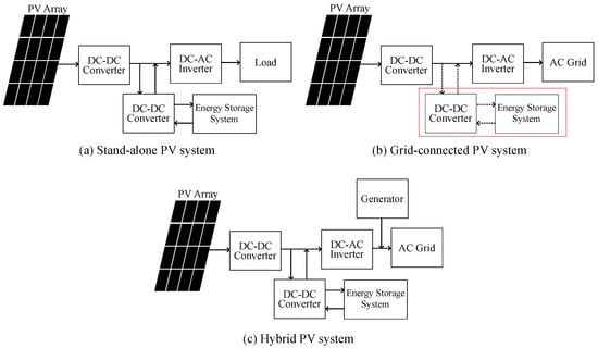
Figure 3.
Different configurations of PV power systems.
2.3. Photovoltaic Power Curtailment Methods
The integration of the PV power will influence the power system’s frequency because PV power highly depends on weather conditions, which are unstable and unpredictable. Providing energy storage systems and introducing power curtailment are the most common solutions for frequency stability problems, as shown in Figure 4a,b. Compared with equipping PV arrays with other energy storage systems, introducing power curtailment is simpler and requires lower initial investment. With power curtailment methods, the PV system is operated at a sub-optimal power level to fulfill the reserve requirement. This means that the operating point of PV systems is below the MPP, thus maintaining a certain amount of power reserves. Therefore, the I-V curve and the actual MPP are essential to be estimated for determining the available power. Several methods have been proposed to solve these estimating problems, categorized into measurement-based and curve-fitting-based methods.

Figure 4.
Alternative PV system controls: (a) with energy storage system, and (b) with power curtailment control algorithm.
The core concept of power curtailment methods based on measurements is that the operating point is measured in real-time with additional sensors, such as temperature and irradiance sensors. Due to accurate measurements, the implementation of the control strategy is effective. However, these additional sensors may increase system cost and complexity.
The main feature of curve-fitting-based methods is that the entire I-V curve is estimated by curve-fitting with several PV output voltage and current samples. Curve-fitting problems can be solved either by the Newton quadratic interpolation (NQI) or the nonlinear least-squares curve-fitting. The accuracy of the NQI, influenced by the selection of three sample points, has been discussed in []. At the same time, the results of the nonlinear least-squares curve-fitting technique are highly affected by initial values and measurement noise, which have been analyzed in detail in [].
In a PV system, the PV array can be operated on the left side or the right side of the MPP, as shown in Figure 5. The left side is located at the left part of the MPP. On the contrary, the right side is allocated on the right part of the MPP. Both sides have advantages and drawbacks []. When operating on the left side of the P-V curve, the PV system can be operated at a wider power range, while the power efficiency of the PV system is higher if operating on the right side.
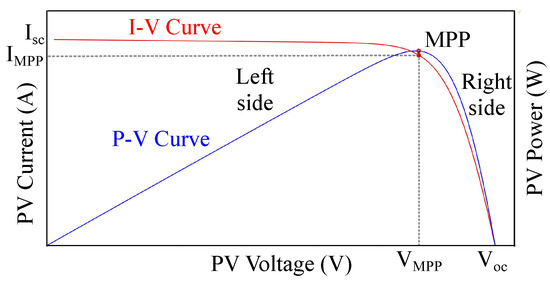
Figure 5.
I-V and P-V characteristics on both sides.
Figure 6 illustrates variations of operating points on both sides of the MPP when the PV power reserves. Before operating on the curtailed mode, the operating point is located at the MPP, denoted by point 1. If weather conditions are constant and the PV system executes the 60% reserve command, there exist two selections of the operating points: point 2 and point 5. When operating on the left side of the MPP, the available PV power drops directly from point 2 to stable point 3 if the irradiance level decreases suddenly, and it then increases to operating point 4 at the 60% reserve command. During this short period, a spike caused by the irradiance change happens. A subsequent increase of irradiance level, if the power reserve command is reduced to zero, will move the operating point to point 8 for satisfying the power demand. Similarly, the operating point falls rapidly on the right side when the irradiance level decreases. In some cases, such as from point 5 to point 6, the operating point may drop to zero, meaning that the PV system does not generate any energy. This is because the open-circuit voltage of the PV array highly depends on the temperature.
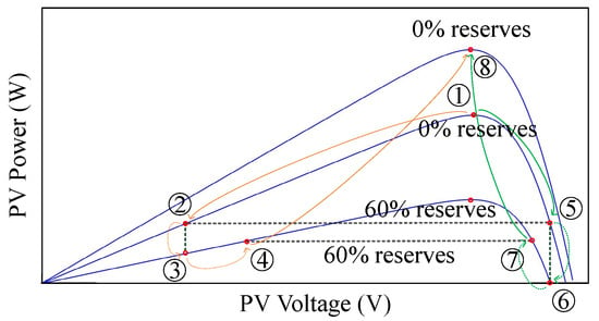
Figure 6.
Variations of operating point when irradiance level changes.
For most proposed methods based on curve-fitting, the operating point only can be situated on the left side or the right side of the MPP. In reference [], a photovoltaic power curtailment method is proposed for operation on both sides of the power-voltage curve. Photovoltaic voltage control with a small-signal model of the boost converter and the real-time nonlinear least-squares curve-fitting is applied in this method. A solution for optimizing curve-fitting problems has been introduced. When the irradiance level changes suddenly, the operation point is situated on the left side of the MPP, whereas if the curtailment is long enough for the temperature level to change, the PV system is operated on the right side of the MPP. The performance of the PV system has been discussed in detail. This paper expands the above mentioned work to consider the converter losses as explained in Section 3.
3. Photovoltaic Power Curtailment Method with Converter Losses
This section introduces the arrangement of a grid-connected PV power system for simulation, the PV power curtailment method proposed in [] and the PV power curtailment method to consider converter losses as well as the control scenario. The discussions of power losses and the efficiency curve are included.
3.1. Arrangement of Grid-Connected PV Power System
Figure 7 shows the topology of a grid-connected PV system with a two-stage converter and a grid filter. Boost converter in the two-stage converter is used to boost the output voltage of the PV array, following with DC/AC inverter that transforms the DC current/voltage into AC, connecting the PV array to the AC grid. The PV voltage control system implements the PV power curtailment method and maximum power point tracking of grid power (ACMPPT) to satisfy the AC grid requirement. In contrast, a voltage source converter (VSC) control algorithm is applied to maintain the DC link voltage and the unity power factor (PF).
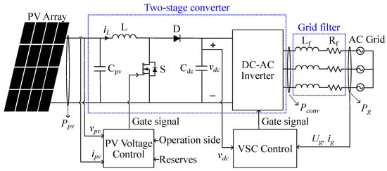
Figure 7.
Topology of grid-connected PV system.
3.2. Power Curtailment Method
Unlike other methods in literature, the power curtailment method proposed in [] allows PV systems to operate on the right and on the left side of the MPP, depending on the needs. Nonlinear least-squares curve-fitting with online voltage and current measurements is used to estimate the temperature and irradiance levels for obtaining IV characteristic by Lambert W function of the SDM which has been stated in Section 2.1.
Nonlinear Least-Squares Curve-Fitting
To estimate the operating point, the nonlinear least-squares curve-fitting is used. In nonlinear least-squares problems, a set of m measurements (, ) is fitted to a nonlinear model by minimizing the vertical distance between the measurements and the model as (6) and (7):
where and is:
Changes in the objective function caused by variations of irradiance and temperature have been discussed in detail in []. The most important result obtained from [] is that the solution is near-perfect if the operating point is around the MPP, while the estimation is far from reality when the PV array is operated at other regions. In other words, there are multiple local minima when the PV system is operated on the left and right sides of the MPP. However, in practice, solar cell temperature dynamics are slower than irradiance dynamics, resulting in solutions that are acceptable on the left and right sides of the MPP.
3.3. Circuit Operation and Losses in Two-Stage Converters
A two-stage converter in a PV system may consist of a boost converter and a three-level bridge inverter. The boost converter boosts PV output voltage, while the three-level bridge inverter transforms the DC current/voltage into AC.
3.3.1. Boost Converter
A boost converter consists of an inductor, a diode, a switch, and two capacitors for boosting up the PV array voltage to fulfill the load requirement, as shown in Figure 8.
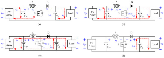
Figure 8.
Operation modes of boost converter: (a) Mode I, (b) Mode II, (c) Mode III, and (d) Mode IV.
The bulky capacitor , installed between the PV array and the boost converter, is used for ripple mitigation. The DC link voltage is held constant by regulating the power flow of the DC link capacitor . For high-frequency switching, a MOSFET can be adopted. The operation of the boost converter can be specified into four modes, depending on the current flowing and the switch operation.
In practice, the boost converter in PV systems may be operated at either the continuous conduction mode (CCM) or the discontinuous conduction mode (DCM), depending on the designed circuit parameters and operating conditions. Theoretical waveforms at CCM and DCM operations of boost converter are shown in Figure 9a,b, respectively. The designed circuit parameters are assumed to be ideal during operation, and the PV array regards as a DC source. The duty ratio d is the ratio of the duration of the increase of the inductor current, (red line), to the total period . For operating at CCM, is operated above zero. For DCM, decreases to zero and represents the ratio of the time is which decreases to zero to .
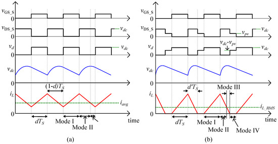
Figure 9.
Theoretical waveformsof boost converter: (a) CCM, and (b) DCM.
Mode I
This mode begins when the switch S is turned on to conduct the inductor current. In this mode, is charged by the PV output voltage, , storing the energy from the PV array. Meanwhile, the stored energy from Mode II releases to the load to cope with the load power requirement. This mode ends when S is switched off.
Mode II
As S is switched off at Mode II, the diode D is forward-biased to conduct the freewheeling current. During this mode, the DC link capacitor is charged by turning on the diode. The energy stored in the inductor L, and the bulky capacitor , flows to . The DC link voltage (blue line) rises, while declines linearly until it cannot fulfill the load power and is less than the output current.
Mode III
In this mode, the inductor current, is less than the output current, . The DC-link capacitor supplies energy to the load with a DC link current, . Mode III ends when decreases to zero.
Mode IV
During this mode for DCM operation, both S and D are turned off. is held at zero. The output energy is supplied by .
3.3.2. Three-Level Bridge Inverter
Figure 10 shows the topology of a three-phase three-level bridge inverter. Each AC output connects to DC+, DC−, and the neutral point N, which is the center point of the DC link. The DC voltage/current transforms to AC by regulating the duty ratio of switches in the three-level bridge inverter. Table 2 lists switch states of the diode-clamped three-level bridge inverter. The output voltage is when switches and are turned on, while is when and are switched on. In N state, is kept at 0 V with turned on switches, and .
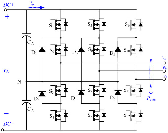
Figure 10.
Topology of three phase three-level bridge inverter.

Table 2.
Switch states of diode-clamped three-level bridge inverter.
3.3.3. Losses in Two-Stage Converters
A PV system is equipped with a power electronic converter to transform the sun’s radiation into electricity. The components in the converter, such as switches, inductors, and capacitors, cause power losses in the PV system, leading to a mismatch between the PV power and the grid one []. Figure 11 shows the topology of the two-stage converter with equivalent series resistances (ESR).
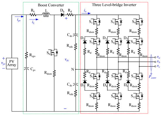
Figure 11.
Topology of two-stage converter with ESR.
Switch
In general, losses produced by power switches can be divided into static losses, including the conduction and cut-off losses, and dynamic losses, including the turn-on and turn-off losses. To simplify the analysis, the essential losses, the conduction and switching losses, are estimated, which are shown in Figure 12 and can be expressed by:
where is the RMS drain current, is the conduction resistance, is the rise time, is the fall time, is the RMS current of power switch, is the drain voltage and is the switching frequency.
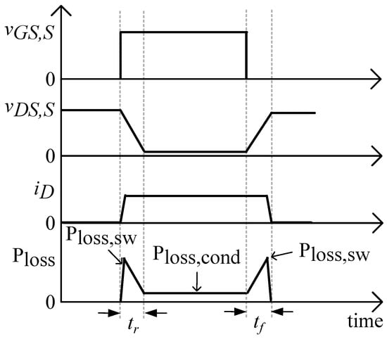
Figure 12.
Conduction and switching losses wave forms.
Diode
For the boost converter, the losses of the diode occur when the diode is turned on with a forward voltage, , to carry the inductor current. During this period, the inductor current decreases. In addition, diode losses in a three-level bridge inverter occur when they are turned on to transform the DC current/voltage to AC. Thus, the losses of diode can be obtained as (10):
where and are the RMS current and the forward voltage of diode, respectively.
Inductor and Capacitor
The inductors and capacitors in converters are responsible for storing the energy from the power source, discharging power to the load, and smoothing the ripple. The power flow among inductors and capacitors causes power losses in the power system. Power losses of the inductor include core losses and winding losses. Core losses depend on several factors, such as peak-peak ripple current, ripple current frequency, core material, core size, and turn count. In contrast, winding losses can be divided into DC and AC winding losses. To simplify the analysis, all losses of an inductor are equivalent to a simple Equivalent Serial Resistance (ESR). Thus, the losses of an inductor can be obtained as (11):
where and are the RMS current and ESR of the inductor, respectively.
Similarly, there are several factors affecting power losses in a capacitor. The losses of a capacitor can be calculated as (12):
where and are the RMS current and ESR of the capacitor, respectively.
3.3.4. Losses in the Grid Filter
In a grid-connected PV system, grid filters are adopted to eliminate the PWM carrier and side-band voltage harmonics generated by the VSC. This can cause some additional losses, . With the unity power factor, can be expressed as (13):
where , and are the grid power, the grid voltage, and the grid filter resistance, respectively.
3.4. Power Curtailment Method Strategy Considering Converter Losses
As stated in Section 2, both operation sides of the P-V curve of a PV module have their advantages and drawbacks. With the benefit of operating on both sides, the SDM and the nonlinear least-squares curve-fitting technique [,] are used in the proposed strategy to estimate the P-V and I-V curves. In addition, in the grid-connected PV power system, the ACMPP and the operating point of the PV array depend on the maximum power point of the PV array (MPP) and the requested grid power, respectively. To compute the ACMPP and the operating point of the PV array for programming the power reserve schedule, the relationship between the grid power and the PV one needs to be calculated. Therefore, losses of the PV system cannot be ignored, including losses in the two-stage converter and the grid filter.
3.4.1. Efficiency Curve of Two-Stage Converters
In a grid-connected grid power system, the irradiance may vary instantaneously, and the load requirement is dynamic, leading to variations of the magnitude of converter output current. This means that the efficiency of the converter is not constant during operation. In practice, detecting the currents of components in a two-stage converter for estimating losses is complex. Instead of detecting the currents, the efficiency curve, calculated by curve-fitting tool [] with several pairs of (, ) values at different irradiance and temperature levels, is used.
Figure 13 shows the static characteristic when the PV array encounters irradiance and temperature changes. Compared with temperature variations, irradiance changes affect the PV voltage more when the PV array is operated at the same power level and on the left side of the P-V curve. This means that the converter’s efficiency influenced by irradiance is higher than by temperature on the left side operation. On the contrary, the PV voltage and the converter efficiency are affected by temperature more than by the irradiance level when operating on the right side of the MPP.

Figure 13.
P-V characteristics of PV array with environmental changes: (a) P-V characteristics of PV array for variations of irradiance, and (b) P-V characteristics of PV array at variations of temperature.
A simple mathematical function may describe the efficiency curve of PV converter:
where is the converter efficiency and a, b, and c are coefficients that need to be determined.
Figure 14 shows the accuracy of the efficiency curve obtained by curve-fitting compared with test points at nominal conditions (25 °C, 1000 W/m) and the left side operation. For validation, a grid-connected PV system with a two-stage converter and a PV array is set up in Simulink to obtain curve-fitting points. In this model, the two-stage converter is formed by a boost converter and a three-level-bridge inverter. The PV array is composed of nine serial and 45 parallel single diode photovoltaic models. The Simulink model and AC grid parameters are further described in Section 4. Table 3 lists the circuit parameters of the two-stage converter for simulation. In this case, the following efficiency equation is obtained:
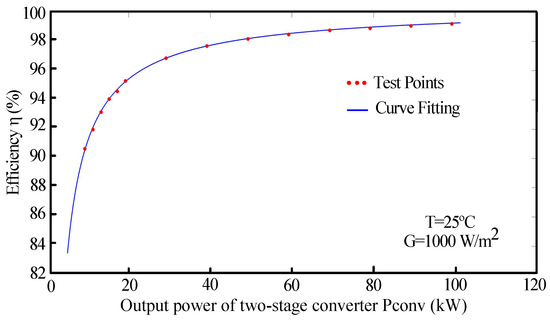
Figure 14.
Comparison of efficiency curve obtained by curve fitting and test points at 25 °C and 1000 W/m.

Table 3.
Circuit parameters of two-stage converter.
The efficiency curve is determined by coefficients a, b and c of Equation (16). Those coefficients are affected by temperature and irradiance. Table 4 lists the values of coefficients with different irradiance at 25 °C, and on the left side operation to find out the relationship between coefficients and irradiance. As it can be seen in Table 4, coefficient a is affected by the irradiance G, whereas coefficients b and c are constant. The value of coefficient a decreases as the irradiance increases. The nonlinear least-squares curve-fitting can estimate the coefficient a dependence with the irradiance:
where G is the irradiance (W/m).

Table 4.
Coefficients with different irradiance and on left side operation.
Coefficients a, b and c at 1000 W/m and on the left side operation but at different temperature levels are listed in Table 5. Similarly, coefficient c is influenced by temperature according to:
where T is the temperature T (°C).

Table 5.
Coefficients with different temperature and on left side operation.
Figure 15 shows the efficiency curve for different irradiance and temperature levels when operating on the left side of the MPP. The efficiency decreases as the irradiance increases, while a slight decrease occurs in efficiency with increases of temperature when operating at the same power level, as shown in Figure 15a,b, respectively.

Figure 15.
Efficiency curve with various weather conditions when operating on left side of MPP: (a) - curve with different irradiance, and (b) - curve with different temperature.
3.4.2. Curve
In some applications, such as power smoothing or power reserve control, grid-connected PV systems need to be operated in the curtailed mode. To obtain the operating point of the PV array when the grid power reserves, the entire P-V curve, the entire curve, the ACMPP, and the MPP need to be calculated. The nonlinear least-square curve-fitting technique is used to obtain the P-V curve and the MPP, while it is important to calculate power losses of the system for estimating the curve and the ACMPP. The relationship among , and the losses, and , can be obtained by (21):
The efficiency curve of the two-stage converter, calculated by Equations (14) and (15), is used to estimate the curve. Hence, Equation (21) can be expressed by (22):
where , , , and are the converter efficiency, the grid power, the grid voltage and resistance, respectively.
Figure 16 shows the curve, the P-V curve and the efficiency curve of the system at 25 °C 1000 W/m and on the left side operation. Once the curve is estimated, the voltage reference can be obtained to implement the PV voltage control. The ACMPP and the efficiency curve can also be calculated to schedule the control system for operating the power system effectively.
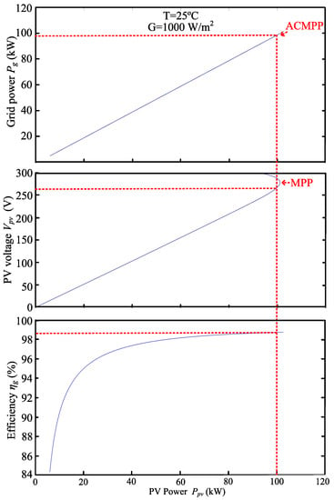
Figure 16.
, P-V and efficiency curves of PV system operating on left side of MPP.
3.5. Control Scheme of Power Curtailment Method Considering Converter Losses
The block diagram of the power curtailment method proposed is shown in Figure 17. The power curtailment method [], which is marked a blue line, is improved with the consideration of converter losses, which is marked by the red dashed line in this control scheme. The PV current, , and the PV voltage, , are detected for implementing the lsqnonlin function. Once nonlinear least-squares curve-fitting problems are solved, the achieved temperature, and irradiance, are obtained. Then, the actual P-V and I-V curves can be depicted, and the MPP is identified by using the IV equation of the SDM with Lambert W function expressed in Equation (5).
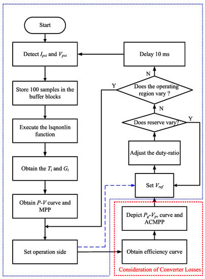
Figure 17.
Control scenario of proposed power curtailment method [] (remarked with blue dashed line) with converter losses (remarked with red dashed line).
For the curtailment method [], after setting the operation side, the PV voltage reference can be obtained directly, which is denoted by the blue dashed arrow without consideration of two-stage converter losses. This means a mismatch may occur between the actual AC power and the required one. For the new proposed method, the two-stage converter efficiency curve can also be estimated by Equation (20) after obtaining and . According to the two-stage converter efficiency curve and the obtained actual P-V curve, the curve can be estimated if the operation side command is set. As a result, the PV voltage reference is acquired to adjust the duty ratio at which the two-stage converter is operated to cope with the reserve requirement. The PV voltage reference is reset when the power reserve command or operating region varies. Every 10 ms, the Matlab function executes the lsqnonlin function and solves nonlinear least-squares curve-fitting problems to respond rapidly to environmental condition changes.
4. Implementation and Validation in MATLAB/Simulink
This section presents the grid-connected PV system model constructed in MATLAB/Simulink and a case study at 25 °C for the left side operation. To verify the effectiveness of the control strategy, the irradiance level on the PV panel is suddenly increased or decreased for emulating the unexpected variation in ambient conditions. The reserve ratio also varies for analyzing the performance of the control system.
4.1. Grid-Connected PV System Model
A model for a 100 kW grid-connected PV system with a two-stage converter is set up in Simulink, adapted from [], as shown in Figure 18, to verify the effectiveness of the control strategy presented in the previous section. The resistances attached to the components of the two-stage converter and the grid filter simulate the losses of the power system. The PV voltage control system cooperates with the VSC controller to implement the control scheme. The designed circuit parameters of the two-stage converter and the AC grid are shown in Table 3 and Table 6, respectively.
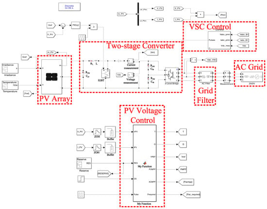
Figure 18.
Grid-connected PV system model.

Table 6.
AC grid parameters.
4.1.1. PV Voltage Control
The instantaneous output voltage and current of the PV array detected by the measurements blocks are transferred to the PV voltage control system. Two Zero Order Hold (ZOH) blocks, with a sampling frequency of 10 kHz, are used for discretizing the measurements, and following with two 100-sample buffer blocks that store these measurements to solve the nonlinear least-squares curve-fitting problems. The Matlab function receives sample data, the active reserve command, and the desired operation side for carrying out the proposed power curtailment method. As a result, the estimated temperature and irradiance, the ACMPP, and the MPP are obtained to investigate system performance. The voltage reference can also be calculated into the PID controller for generating the duty cycle. The PID controller’s output values are compared with a triangle waveform to generate the gating signal for switching the IGBT. Accordingly, the boost converter can be controlled to implement the control scheme.
4.1.2. Three-Level Voltage Control
The VSC control system continuously receives grid currents, grid voltages, and the DC link voltage from the measurement blocks, as shown in Figure 19. These instantaneous current and voltage measurements are transformed through abc to Alpha-Beta-Zero blocks, Alpha-Beta-Zero to dq0 blocks, and PID controller for implementing two VSC control system control loops: external and internal control loops. The outer control loop maintains the 500V DC link voltage while the inner control loop regulates and grid currents to keep the unity power factor. current reference from the DC link voltage controller is used for the regulation of the active power. current reference is set to zero to eliminate the reactive power flowing to the grid. As a result, three modulating signals are obtained to generate the PWM signal that controls DC/AC converter.
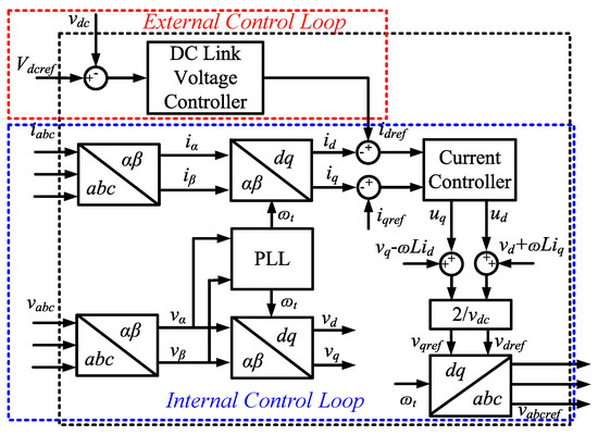
Figure 19.
VSC control.
4.2. Case Study
In this case, the environmental temperature is held constant at 25 °C, and operating points of the PV array are on the left side of the MPP. To investigate the performance of the proposed method, the PV array is operated under variable irradiance levels, as shown in Figure 20a. In this figure, the irradiance level, estimated through the nonlinear least-squares curve-fitting technique, tracks the actual irradiance accurately.
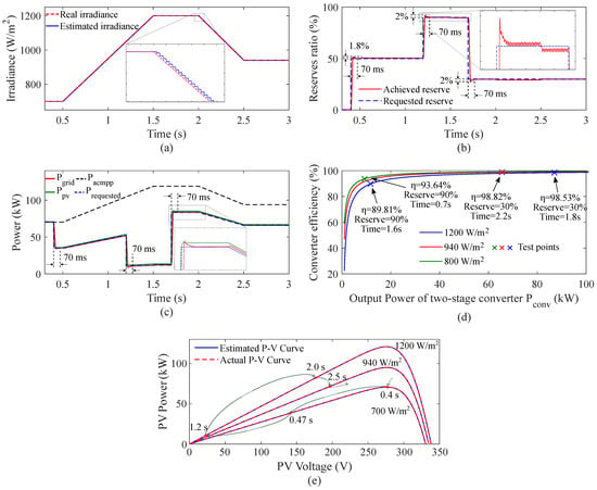
Figure 20.
Simulation results: (a) Irradiance evolution, (b) power reserves evolution, (c) power evolution, (d) two-stage converter efficiency, and (e) estimated and actual P-V curve.
Figure 20b illustrates the reserve level variations, which are limited from 0% to 90%. It is noticeable that, when the PV system is subject to step changes of the power reserve command at 0.4 s, 1.2 s and 1.7 s, tiny spikes of less than 2%, with a short response time of 0.07 s, occur. The power system needs a short response time to adapt to the new operating point if the demanding command changes. However, the achieved reserve matches the requested reserve successfully in a steady-state, meaning the control system effectively carries out the proposed power curtailment method.
Figure 20c shows the power evolution, including the ACMPP, the grid power, the PV power, and the required power. The actual grid power, denoted by the red line, almost coincides with the requested grid one, denoted by the dashed blue line, while the PV power, denoted by the green line, is higher than the grid power because of the losses in the power system. This means that the variable power reserve command can be achieved perfectly. To clarify the advantages of considering power converter losses, let us compare the power available at the dc side and the one at the ac side. In the zoomed part of Figure 20c, near s, the PV power is 85.1 kW whereas the available power at the grid side is 83.5 kW. This means that the error committed by strategies that disregard power converter losses is approximately in this case.
Figure 20d illustrates the converter efficiency obtained by simulation. The blue, red and green lines are obtained from Equation (16), while test points are calculated from the simulation at different reserve commands (30%, 90%) and irradiance levels (800 W/m, 940 W/m, 1200 W/m). The near-perfect match of test points to the estimated lines can be observed in this figure.
Figure 20e shows the comparison of the estimated (blue line) and the actual P-V curve (dashed red line) at different irradiance levels (700 W/m, 940 W/m, 1200 W/m). As can be seen, the estimated P-V curve accurately represents the actual P-V curve. The operating point trajectories can also be seen in this figure. At 0.4 s, the PV system receives the 50% reserve command. Then, the operating point moves from the MPP to a suboptimal power point with a 70 ms delay. From 0.47 s to 1.50 s, the irradiance level and the reserve command change from 700 W/m to 1200 W/m and from 50% to 90%, respectively. After that, the irradiance level keeps constant with 1200 W/m until 2.0 s. During this period, the reserve command varies from 90% to 30%, resulting in variations of the voltage reference from 24 V to 180 V. From 2.0 s, the PV system is constantly operated at the 30% reserve command. The suboptimal power varies from 65 kW to 81 kW caused by the variations of the irradiance level from 1200 W/m to 940 W/m.
The estimated PV voltage, current, and the PVMPP are shown in Figure 21. The variations of PV voltage and current depend on the reserve ratio and irradiance.

Figure 21.
PV array outputs: (a) PV output voltage evolution, and (b) PV output current evolution.
Figure 22 shows the results of the grid side of the PV system. In steady-state, the DC link voltage ripple is lower than 0.3%, as shown in Figure 22a,b. The worst case, with the DC link voltage (527 V) happens when the reserve command changes suddenly at 1.7 s. During this period, the DC link voltage ripple is 5.5%. Figure 22c illustrates the grid power ripple. The fluctuation of the grid power is affected by the irradiance and the reserve levels. Compared with the 90% reserve level from 1.5 s to 1.7 s, the grid power ripple at the 30% reserve level from 1.7 s to 2.0 s can be negligible. During 0.5–1.5 s and 2.0–2.5 s, the irradiance level varies continuously, causing variations of the grid power ripple value. The line grid currents are depicted in Figure 22d.
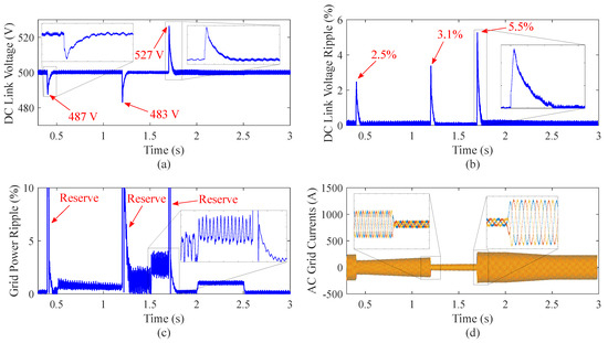
Figure 22.
Grid side magnitudes: (a) DC link voltage, (b) DC link voltage ripple evolution, (c) ripple of grid power, and (d) grid current.
5. Conclusions and Discussion
The power curtailment method proposed in [] for operation on both sides of the power-voltage curve has been improved with consideration of the losses in the PV system. To estimate the losses of the PV power system, the efficiency curve is calculated by nonlinear least-squares curve-fitting.
The control strategy is simulated to analyze the PV system’s performance. From the simulation results, the following observations and conclusions are noteworthy:
- The single diode model with the Lambert W function accurately represents the Matlab Electrical Simscape model.
- The efficiency curve, estimated by nonlinear least-squares curve-fitting with several samples in real-time at different temperature and irradiance levels, is accurate for calculating the losses of the PV power system.
- The two-stage converter efficiency is mainly affected by the irradiance levels when the PV power system operates on the left side of the MPP. On the contrary, the temperature levels influence the converter efficiency significantly when working on the right side of the P-V curve.
- The control strategy with the power curtailment method is implemented effectively when operating on the left side of the MPP with variations of irradiance. The actual AC grid power tracks the grid power requirements successfully.
The proposed method improves the estimation accuracy of the output characteristic of a PV system when it is subject to power curtailment. This improvement is expected to have a positive impact in the participation of PV systems on frequency control. However, the proposed methodology has been validated just for a specific PV system configuration, being constituted by a single boost converter and a single inverter. Future studies should investigate the performance of the proposed method while considering different topologies, as well as power converters of different nominal power and characteristic parameters. The authors also recommend validating the proposed methodology experimentally. In this way, empirical expressions can be obtained for the power converter losses and incorporated to the control system. Further research could include the assessment of this impact on frequency stability, particularly in weak electric power systems with a high share of solar photovoltaic plants.
Author Contributions
Conceptualization, J.M.R.-D. and S.M.; Data curation, D.Y.; Formal analysis, J.M.R.-D. and S.M.; Funding acquisition, S.M.; Investigation, D.Y. and J.M.R.-D.; Methodology, J.M.R.-D. and S.M.; Project administration, S.M.; Software, D.Y.; Supervision, S.M.; Validation, D.Y.; Visualization, D.Y. and J.M.R.-D.; Writing—original draft, D.Y., J.M.R.-D. and S.M.; Writing—review & editing, J.M.R.-D. and S.M. All authors have read and agreed to the published version of the manuscript.
Funding
This research was funded by the Spanish national research agency Agencia Estatal de Investigación, grant number PID2019-108966RB-I00 /AEI/ 10.13039/501100011033.
Conflicts of Interest
The authors declare no conflict of interest.
Abbreviations
The following abbreviations are used in this manuscript:
| ACMPPT | Maximum Power Point Tracking of Grid Power |
| CPG | Constant Power Generation |
| CCM | Continuous Conduction Mode |
| DCM | Discontinuous Conduction Mode |
| ESR | Equivalent Series Resistance |
| MPP | Maximum Power Point |
| MPPT | Maximum Power Point Tracking |
| NQI | Newton Quadratic Interpolation |
| PV | Photovoltaic |
| PF | Power Factor |
| PWM | Pulse Width Modulation |
| SDM | Single-Diode Model |
| VSC | Voltage Source Converter |
| ZOH | Zero Order Hold |
References
- Blaabjerg, F.; Yang, Y.; Ma, K. Power electronics—Key technology for renewable energy systems—Status and future. In Proceedings of the 2013 3rd International Conference on Electric Power and Energy Conversion Systems, Istanbul, Turkey, 2–4 October 2013; pp. 1–6. [Google Scholar] [CrossRef] [Green Version]
- Dhople, S.V.; Davoudi, A.; Nilles, G.; Chapman, P.L. Maximum power point tracking feasibility in photovoltaic energy-conversion systems. In Proceedings of the 2010 Twenty-Fifth Annual IEEE Applied Power Electronics Conference and Exposition (APEC), Palm Springs, CA, USA, 21–25 February 2010; pp. 2294–2299. [Google Scholar] [CrossRef]
- Sangwongwanich, A.; Yang, Y.; Blaabjerg, F. A Sensorless Power Reserve Control Strategy for Two-Stage Grid-Connected PV Systems. IEEE Trans. Power Electron. 2017, 32, 8559–8569. [Google Scholar] [CrossRef] [Green Version]
- Ghosh, S.; Rahman, S.; Pipattanasomporn, M. Distribution Voltage Regulation Through Active Power Curtailment with PV Inverters and Solar Generation Forecasts. IEEE Trans. Sustain. Energy 2017, 8, 13–22. [Google Scholar] [CrossRef]
- Fang, J.; Li, H.; Tang, Y.; Blaabjerg, F. On the Inertia of Future More-Electronics Power Systems. IEEE J. Emerg. Sel. Top. Power Electron. 2019, 7, 2130–2146. [Google Scholar] [CrossRef]
- Mohandes, B.; Moursi, M.S.E.; Hatziargyriou, N.; Khatib, S.E. A Review of Power System Flexibility with High Penetration of Renewables. IEEE Trans. Power Syst. 2019, 34, 3140–3155. [Google Scholar] [CrossRef]
- Sigrist, L.; Egido, I.; Lobato Miguélez, E.; Rouco, L. Sizing and Controller Setting of Ultracapacitors for Frequency Stability Enhancement of Small Isolated Power Systems. IEEE Trans. Power Syst. 2015, 30, 2130–2138. [Google Scholar] [CrossRef]
- Nguyen, N.; Mitra, J. Effect of wind power on load frequency control. In Proceedings of the 2016 IEEE Power and Energy Society General Meeting (PESGM), Boston, MA, USA, 17–21 July 2016; pp. 1–5. [Google Scholar] [CrossRef]
- Batzelis, E.I.; Anagnostou, G.; Cole, I.R.; Betts, T.R.; Pal, B.C. A State-Space Dynamic Model for Photovoltaic Systems with Full Ancillary Services Support. IEEE Trans. Sustain. Energy 2019, 10, 1399–1409. [Google Scholar] [CrossRef] [Green Version]
- Van de Vyver, J.; De Kooning, J.D.M.; Meersman, B.; Vandevelde, L.; Vandoorn, T.L. Droop Control as an Alternative Inertial Response Strategy for the Synthetic Inertia on Wind Turbines. IEEE Trans. Power Syst. 2016, 31, 1129–1138. [Google Scholar] [CrossRef]
- Crăciun, B.I.; Kerekes, T.; Séra, D.; Teodorescu, R. Frequency Support Functions in Large PV Power Plants with Active Power Reserves. IEEE J. Emerg. Sel. Top. Power Electron. 2014, 2, 849–858. [Google Scholar] [CrossRef]
- Omran, W.A.; Kazerani, M.; Salama, M.M.A. Investigation of Methods for Reduction of Power Fluctuations Generated From Large Grid-Connected Photovoltaic Systems. IEEE Trans. Energy Convers. 2011, 26, 318–327. [Google Scholar] [CrossRef]
- Batzelis, E.I.; Kampitsis, G.E.; Papathanassiou, S.A. Power Reserves Control for PV Systems with Real-Time MPP Estimation via Curve Fitting. IEEE Trans. Sustain. Energy 2017, 8, 1269–1280. [Google Scholar] [CrossRef]
- Sangwongwanich, A.; Yang, Y.; Blaabjerg, F.; Sera, D. Delta Power Control Strategy for Multistring Grid-Connected PV Inverters. IEEE Trans. Ind. Appl. 2017, 53, 3862–3870. [Google Scholar] [CrossRef] [Green Version]
- Hoke, A.F.; Shirazi, M.; Chakraborty, S.; Muljadi, E.; Maksimovic, D. Rapid Active Power Control of Photovoltaic Systems for Grid Frequency Support. IEEE J. Emerg. Sel. Top. Power Electron. 2017, 5, 1154–1163. [Google Scholar] [CrossRef]
- Li, X.; Wen, H.; Zhu, Y.; Jiang, L.; Hu, Y.; Xiao, W. A Novel Sensorless Photovoltaic Power Reserve Control with Simple Real-Time MPP Estimation. IEEE Trans. Power Electron. 2019, 34, 7521–7531. [Google Scholar] [CrossRef]
- Riquelme-Dominguez, J.M.; Martinez, S. A Photovoltaic Power Curtailment Method for Operation on Both Sides of the Power-Voltage Curve. Energies 2020, 13, 3906. [Google Scholar] [CrossRef]
- Moo, C.S.; Wu, G.B. Maximum Power Point Tracking with Ripple Current Orientation for Photovoltaic Applications. IEEE J. Emerg. Sel. Top. Power Electron. 2014, 2, 842–848. [Google Scholar] [CrossRef]
- Esram, T.; Kimball, J.; Krein, P.; Chapman, P.; Midya, P. Dynamic maximum power point tracking of photovoltaic arrays using ripple correlation control. IEEE Trans. Power Electron. 2006, 21, 1282–1291. [Google Scholar] [CrossRef]
- Hsieh, Y.C.; Yu, L.R.; Chang, T.C.; Liu, W.C.; Wu, T.H.; Moo, C.S. Parameter Identification of One-Diode Dynamic Equivalent Circuit Model for Photovoltaic Panel. IEEE J. Photovolt. 2020, 10, 219–225. [Google Scholar] [CrossRef]
- Petrone, G.; Spagnuolo, G.; Ramos-Paja, C.A.; Spagnuolo, G.; Vitelli, M.; Xiao, W. Photovoltaic Sources Modeling, 1st ed.; John Wiley & Sons, Inc.: Hoboken, NJ, USA, 2017; pp. 10–11. ISBN 978-111-875-612-6. [Google Scholar]
- De Soto, W.; Klein, S.A.; Beckman, W.A. Improvement and validation of a model for photovoltaic array performance. Sol. Energy 2006, 80, 78–88. [Google Scholar] [CrossRef]
- Batzelis, E.I.; Routsolias, I.A.; Papathanassiou, S.A. An Explicit PV String Model Based on the Lambert W Function and Simplified MPP Expressions for Operation Under Partial Shading. IEEE Trans. Sustain. Energy 2014, 5, 301–312. [Google Scholar] [CrossRef]
- Barry, D.A.; Parlange, J.Y.; Li, L.; Prommer, H.; Cunningham, C.J.; Stagnitti, F. Analytical approximations for real values of the Lambert W-function. Math. Comput. Simul. 2000, 53, 95–103. [Google Scholar] [CrossRef]
- Duffie, J.A.; Beckam, W.A. Solar Engineering of Thermal Processes, 4th ed.; John Wiley & Sons, Inc.: Hoboken, NJ, USA, 2013; pp. 747–750. ISBN 978-111-841-812-3. [Google Scholar]
- Demoulias, C. A new simple analytical method for calculating the optimum inverter size in grid-connected PV plants. Electr. Power Syst. Res. 2010, 80, 1197–1204. [Google Scholar] [CrossRef]
- Levenberg, K. A method for the solution of certain non-linear problems in least squares. Q. Appl. Math. 1944, 2, 164–168. [Google Scholar] [CrossRef] [Green Version]
- Hansen, P.C.; Pereyra, V.; Scherer, G. Least Squares Data Fitting with Applications, 1st ed.; The Johns Hopkings University Press: Baltimore, MD, USA, 2013; pp. 147–150. ISBN 978-142-140-858-3. [Google Scholar]
- The MathWorks Inc. Matlab and Electrical Simscape Toolbox; The MathWorks Inc.: Natick, MA, USA, 2020. [Google Scholar]
- Giroux, P.; Sybille, G.; Osorio, C.; Chandrachood, S. Detailed Model of a 100-kW Grid-Connected PV Array. 2022. Available online: https://www.mathworks.com/help/physmod/sps/ug/detailed-model-of-a-100-kw-grid-connected-pv-array.html (accessed on 6 May 2022).
Publisher’s Note: MDPI stays neutral with regard to jurisdictional claims in published maps and institutional affiliations. |
© 2022 by the authors. Licensee MDPI, Basel, Switzerland. This article is an open access article distributed under the terms and conditions of the Creative Commons Attribution (CC BY) license (https://creativecommons.org/licenses/by/4.0/).