Abstract
On-chip memory is one of the core components of deep learning accelerators. In general, the area used by the on-chip memory accounts for around 30% of the total chip area. With the increasing complexity of deep learning algorithms, it will become a challenge for the accelerators to integrate much larger on-chip memory responding to algorithm needs, whereas the on-chip memory for multiprecision computation is required by the different precision (such as FP32, FP16) computations in training and inference. To solve it, this paper explores the use of single-port memory (SPM) in systolic-array-based deep learning accelerators. We propose transformation methods for multiple precision computation scenarios, respectively, to avoid the conflict of simultaneous read and write requests on the SPM. Then, we prove that the two methods are feasible and can be implemented on hardware without affecting the computation efficiency of the accelerator. Experimental results show that both methods have about 30% and 25% improvement in terms of area cost when accelerator integrates SPM without affecting the throughput of the accelerator, while the hardware cost is almost negligible.
1. Introduction
Machine learning is the process of making computer systems learn without explicit instructions by analyzing and drawing inferences from data patterns using algorithms and statistical models. One of the major limitations of artificial intelligence and machine learning has always been computational power, which has been a cause of concern for researchers. CPUs were not as powerful and efficient a few decades ago when it came to running large computations for machine learning. Nowadays, in the explosive growth of data, the deep-learning-alone method can not fulfill the demands of researchers, while the massive cost, energy consumption, and data processing time of using the deep-learning-alone method have become a commonplace. In order to break this bottleneck, the AI accelerator, is created which is a powerful machine learning hardware chip that is specifically designed to run artificial intelligence and machine learning applications smoothly and swiftly.
In order to reduce the overhead of off-chip memory access [1,2,3,4] thus improving the computational efficiency, state-of-the-art deep learning accelerators [5,6] integrate a large amount of on-chip memory to save interlayer features or weights. Taking Google TPU v1 [7,8] as example, as shown in Figure 1, it can be seen that the unified buffer dominates the area cost of the chip. However, large on-chip memory can inevitably lead to low processing-in-memory (PIM) [9,10,11,12,13,14] cost, which limits the accelerators computing efficiency. There are some methods to solve this problem, and the most common way is moving the on-chip memory to the off-chip area. Although this method can greatly increase the area cost of processing units, it increases the overhead of moving data from off-chip to on-chip which can not be ignored. Some researchers have developed model compression algorithms [15,16,17,18,19] to reduce the memory demand of neural networks at the cost of network accuracy. Differently, we aim to reduce of area cost of on-chip memory in the aspect of the memory device.
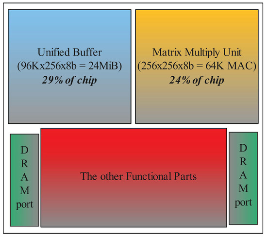
Figure 1.
The structure of TPU.
In general, there are three types of memory intellectual property (IP) cores, including single-port (SP), two-port (TP), and dual-port (DP) memory. Although SP memory has the lowest area overhead, it can only support one memory read or write access at a time. However, both TP- and DP-based memory can support simultaneous read and write requests (for TP-based memory, it is required that the addresses of the read and write requests are different).
Systolic arrays (SA) are hardware structures built for fast and efficient operation of regular algorithms that perform the same task with different data at different time instants. Systolic arrays replace a pipeline structure with an array of processing elements that can be programmed to perform a common operation. Regularity, reconfigurability, and scalability are some of the features of systolic design. Systolic architectures offer the competence to uphold the high-throughput capacity requirement, and nowadays are widely used in deep learning accelerators [20,21,22,23,24]. The dataflow in the existing SA-based AI accelerator can be roughly divided into two types: weight stationary (WS) and output stationary (OS) [25,26]. In both WS and OS, the on-chip buffer would be read and written by SA simultaneously. Especially in WS, the temporary data are frequently delivered between SA and the on-chip buffer. So, TP is widely applied on the on-chip buffer. In order to decrease the on-chip space area cost, we implement the on-chip buffer with single-port memory (SPM) instead of two-port memory (TPM). However, while applying SPM, scenarios of bank conflict [27,28,29] (reading and writing happen in the same buffer bank simultaneously) will inevitably happen.
Nowadays, many researchers are exploring lower precision computation to improve computing throughput in accelerators (e.g., single-precision, mixed-precision, half-precision). Computations with different precision computations are the general trend. In order to support different precision computations in systolic-array-based accelerators, we need to design an efficient addressing mapping module for single- as well as multiprecision computations.
In this work, due to the feature that SP cannot be read and written simultaneously, we propose a series of novel address transformation methods based on SPM supporting single-precision, mixed-precision, and half-precision computation. The basic idea of these methods is changing the address mapping [30] of data written to the bank storing the intermediate results between off-chip and on-chip memory. In addition, this is because the address transformation methods will inevitably generate the conflicts. So, we also propose a conflict-embracing method, as well as hardware, without affecting the correctness of the results.
The contributions of this paper are as follows:
- We propose an address transformation method which enables the effectively integration of SPM and greatly saves the area cost of systolic-array-based accelerators on-chip. We further propose a novel address transformation method to adapt multiple precision computation which can effectively improve computing efficiency.
- We design a small module in the existing AI accelerator which uses hardware-friendly logic. The module consists of two main features: addressing mapping and conflict handling. The additional module increases several computation time overhead which can be ignored while containing the correctness of the computation.
- We implement SPM-based designs on RTL with a 7 nm library and evaluate with various real data. Experimental results show that Our SPM-based designs achieve about 30% and 25% improvement in area cost without affecting the throughput of the accelerator.
2. Background
2.1. Systolic-Array-Based Accelerators Structure
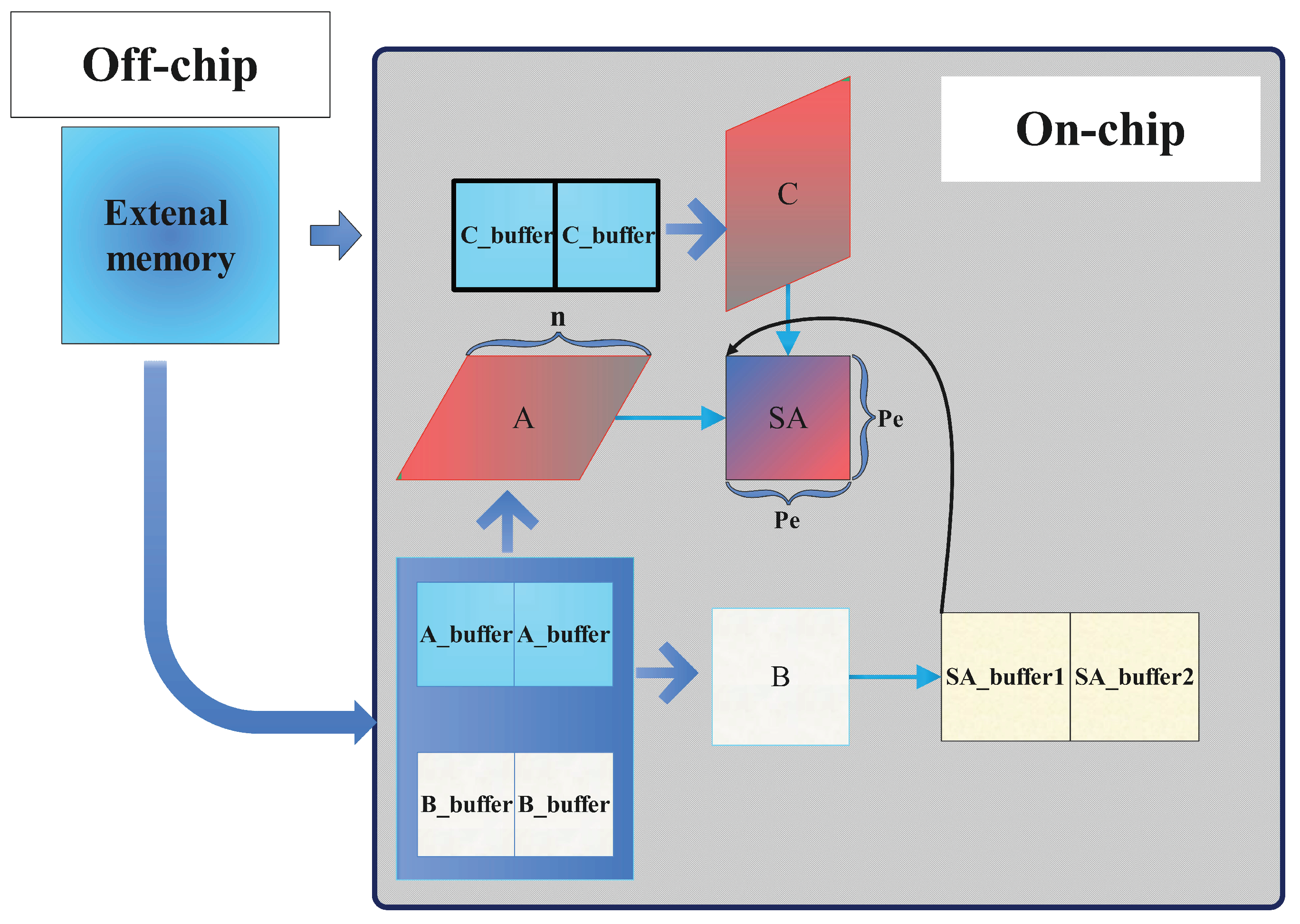
Figure 2 illustrates the basic architecture of 2D systolic-array-based deep learning accelerator [31,32,33,34], which consists of processing elements (PEs). Each PE has a corresponding buffer to store weights, partial sums, and activation. Matrix A represents the input image matrix, while matrix B is the weight matrix. Matrix C stores the intermediate results, and the initial data of the three buffers A, B, and C are fetched from the external memory (such as high-bandwidth memory (HBM)) [35]. Matrices A and B are read from the on-chip buffer and matrix C is used to store the initial deviation and the intermediate result of the calculation simultaneously. Due to the size limitations of the systolic array and network parameters, there are a large number of intermediate results for subsequent calculations. By setting two buffers on the chip to store matrix C, we reduce data transmission between on-chip and off-chip.
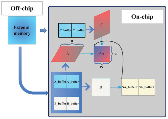
Figure 2.
The 2D systolic array accelerator architecture.
When computing, the weight matrix is passed to SA from left to right, and the data matrix C is also passed to SA from top to bottom after the data in SA_buffer is ready. It should be noted that both matrix A and matrix C have changed from a rectangle to a parallelogram. Then, for the computing results there is another transform module to receive the results and send them back into C-buffer. This is because in a systolic array, the time taken to operate and the time required to transfer data are different. This input method is beneficial to the systolic array; it ensures that the longitudinal partial transmission and the horizontal original data transmission occur simultaneously during the calculation process, and it further ensures the efficient operation of the systolic array and the correctness of the calculation results.
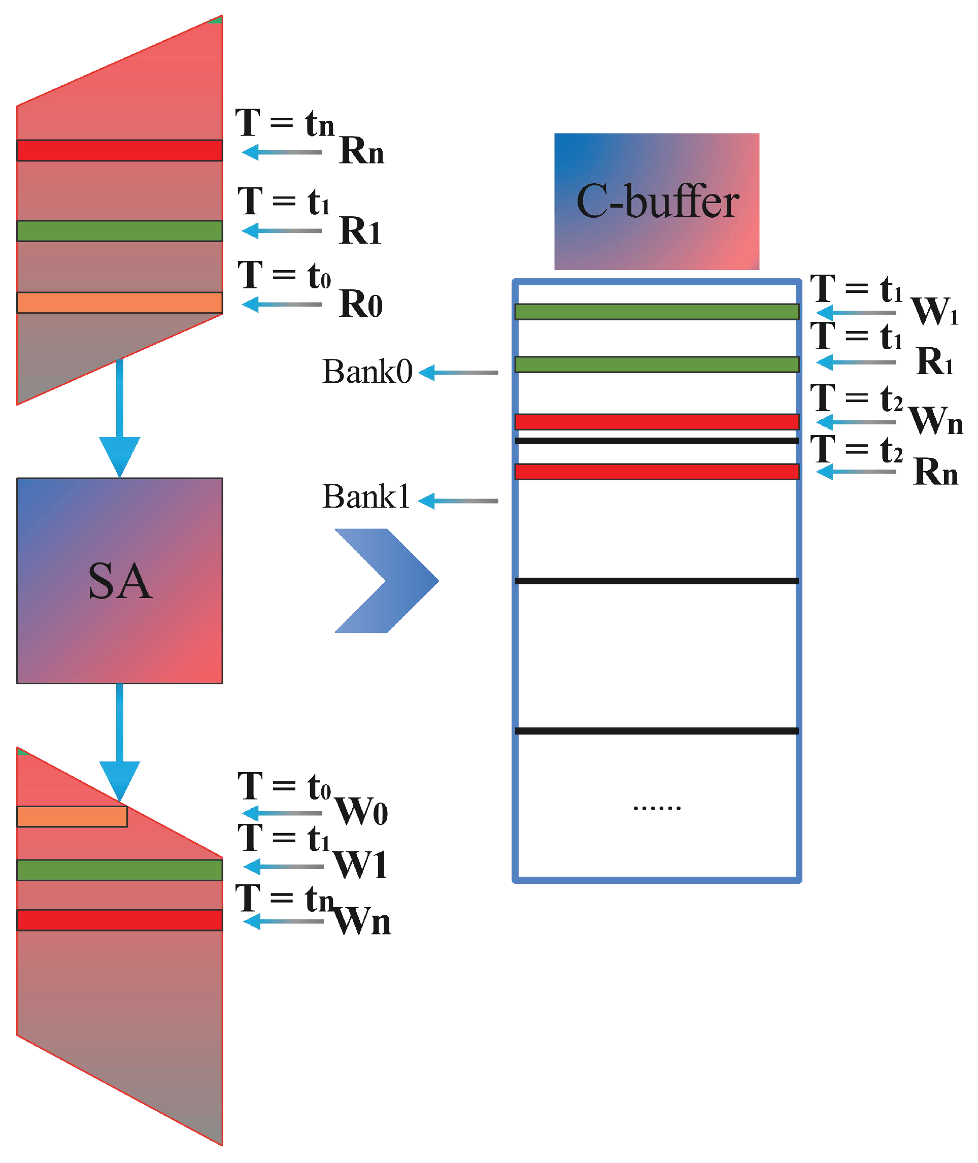
2.2. The Conflicts of Memory Access to SPM
Since TPM banks require additional interface and addressing logics than SPM, this causes the space occupied by TPM to be much larger than that of SPM. Compared with TPM, SPM cannot read and write simultaneously. There are problems that inevitably occur. Therefore, some special read-and-write sequences are needed to ensure that they cannot appear in the same bank in the C-buffer simultaneously. This is also the main source of the address arrangement in the paper. The specific situation is shown in Figure 3. We can see that at , the upper input C needs to read bank0, which corresponds to a certain row in bank0 that needs to be written to the data just calculated. At this time, SPM cannot be performed simultaneously. At , the upper input C also needs to read bank1 (), while the output C is writing a row in the bank0 () simultaneously. The first case causes read–write conflicts, but the second does not. The conflict can only be reflected in the SPM, so the question of how to resolve this conflict is the focus of this paper.

Figure 3.
The conflict when C is written and read in SA.
2.3. The Area Cost of SPM and TPM
We have obtained different effects on the space cost of the C-buffer by changing the size (depth) of the bank. For the computation of the C-buffer space overhead, the space occupied by SPM and TPM in different banks is generated according to the software. As shown in Table 1, for different depths, the space occupied by SPM relative to TPM is optimized to different degrees. However, this optimization is not linear. The main reason is that, in the hardware design, the greater the bank depth, the more complex the address lines required for TPM, which also causes the TPM and SPM memory to continue to expand. However, when the depth reaches a certain value, although SPM saves a greater area compared with TPM, the ratio value shrinks instead. This is also because when the SPM area itself is large, this makes SPM relative to the area obtained by TPM. The proportion of dominance can be reduced; therefore, the space saving is not as large as it seems. So, in this paper we will also discuss the scalability of SPM.

Table 1.
The influence of different banks on space overhead.
2.4. Multiprecision Computation
In order to pursue higher performance computing speed, many researchers have begun to apply lower precision data for convolution computation. Moreover, NVIDIA A100 Tensor Core GPU [36,37,38] has supported different precision computation, which has already applied multiprecision computation with different memory access patterns [39,40,41,42]. Compared with single-precision floating-point convolution computation, half-precision computing has the advantage of faster computing speed and less memory. Note that, in Figure 4c, for the multiprecision computation, the input data in matrix A and B is FP16, the results (FP32) are obtained by the computing of multiplication with adding the FP32 data in matrix C, the data in matrix C can be biased or middle results, and the output becomes twice as much as the input. So, the memory access patterns need to be doubled.
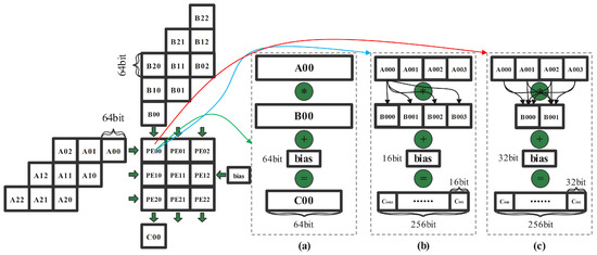
Figure 4.
The half-precision computation mode: (a) baseline; (b) the half-precision computation; (c) the multiprecision computation.
According to the improvement by NVIDIA Tensor Core for data computation in Table 2 [37], the throughput of the FP16 data’s computation commands more than 16 times that of the FP64 data computation, which puts forward a higher requirements for memory access patterns. The computation process is as follows: Figure 4b shows that both matrix A and matrix C conduct as the input which have changed from a rectangle to a parallelogram, every data block represents 64-bit data which consist of 4 blocks of 16-bit data, and every 16-bit data in the data block are cross-multiplied by the PE in SA (though, in the baseline shown in Figure 4a, every 16-bit data block is multiplied correspondingly), the output of PE is 64 bit∗4. So, the memory access patterns of C-buffer need to be quadrupled.
Table 2.
NVIDIA A100 Tensor Core GPU performance specs.
3. Single-Port Memory Design Ideas for Both Single- and Multi-Precision Computing
In this section, we primarily introduce the data memory method of external memory and C-buffer. We discuss the impact of this memory method, and then propose a design idea for SPM. Section 3.1 gives the data in the buffer and the slice outside memory methods. Section 3.2 describes the impact of data arrangement on SPM and TPM. Section 3.3 describes the conflict while using SPM.
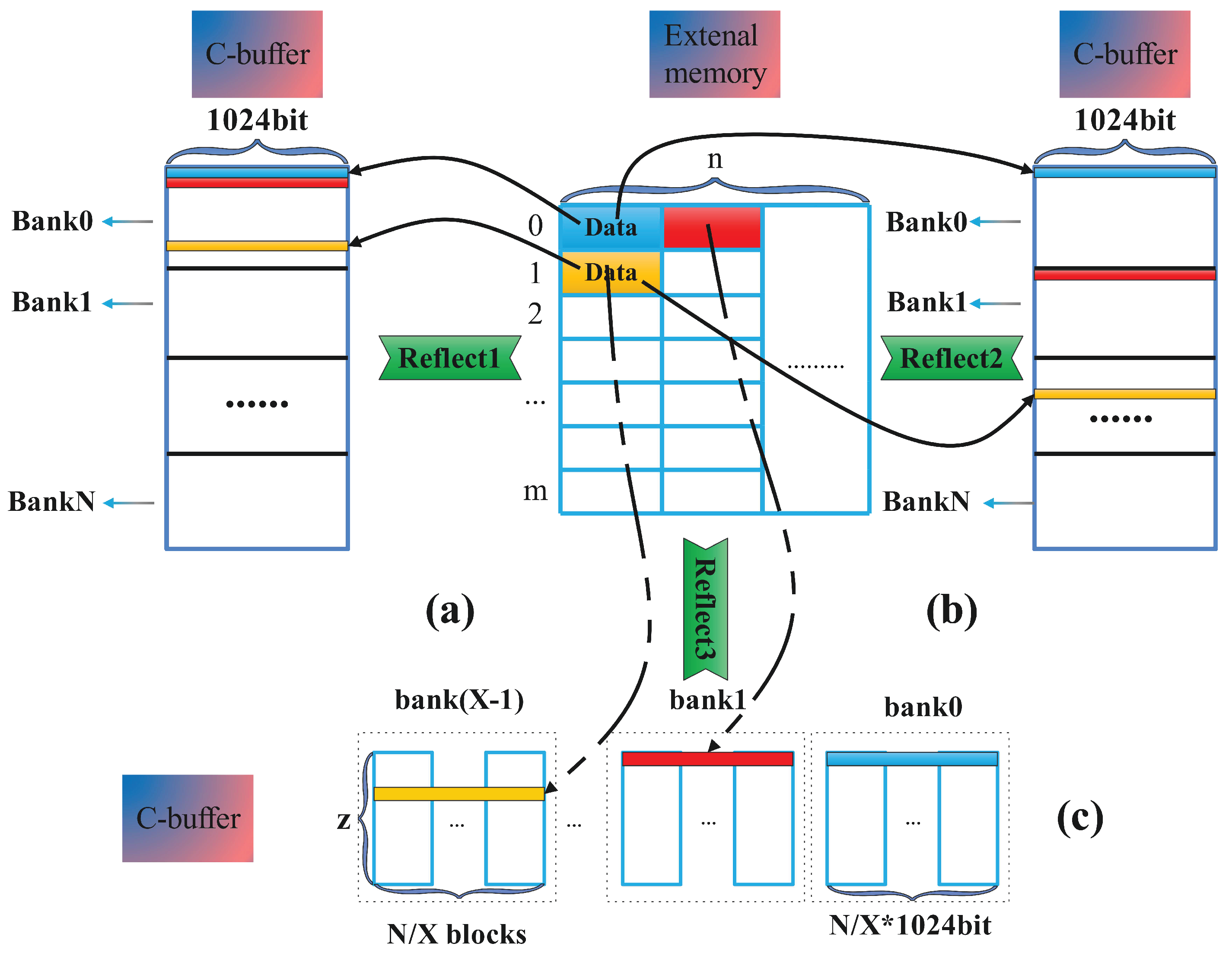
3.1. Data Memory in External Memory and C-Buffer
In the systolic array computation, the three input matrices of A, B, and C need to be cut into a size corresponds to no more than three buffers because the primarily three buffers of A, B, and C have certain space limitations. This is a major premise, so we need to cut the graph before calculating. After cutting the input graph, three parameters——can be obtained. At this time,
where external memory is one for a matrix with a height of m and a width of n, the baseline data memory method is shown in Figure 5a as represented for the C-buffer, the same color in external memory, and C-buffer represents the same data. Generally, the data in the C-buffer are moved in the order of the data in the external memory.
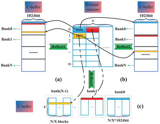
Figure 5.
The mapping methods/algorithms: (a) TPM; (b) SPM; (c) SPM for multiple precision.
3.2. The Impact of Data Arrangement on SPM and TPM
According to Section 2.2, we know that the traditional data arrangement cannot satisfy SPM’s needs, and the method will inevitably lead to endless conflicts that we cannot accept.
In order to prevent this from happening, a novel address arrangement method is needed to ensure that no conflicts occur or to minimize conflicts as much as possible. Here, we propose a unique address arrangement method that can reduce the occurrence of conflicts, to a large extent but which cannot completely avoid conflicts (the conditions for completely avoiding conflicts are strict). Next, we will explain the design of the address-mapping module and the possible conflicts.
According to the aforementioned possible problems of the SPM, if the data are placed in the C-buffer in order, the data in external memory corresponds to the data in C, so the reading and writing of SA to C is also sequential. For the same individual, there tends to be many rows of data (each row of data is 1024 bits), so when SA reads and writes C, it is only when the write signal of the data reads the next body in the read signal can the possibility of simultaneous reading and writing can be guaranteed.
To ensure as few conflicts as possible, we propose an idea for address arrangement: when external memory is moved to the C-buffer, every 16-bit block of data in external memory is regarded as a small block, and multiple consecutive small blocks of data are placed in the same bank, with the subsequent data being placed in the next bank, and so on, so as to ensure the cross-arrangement of the data as much as possible.
Based on this idea, we have designed a model that inevitably generates conflict probability when different numbers of consecutive small blocks are placed in the same bank. The model performs simulation analysis based on the read-and-write interval that may occur in the actual situation; according to the running signal from the waveform, we found that the read–write interval is possible within a range of 1–118. Clearly, it is impossible to avoid conflicts completely with a limited number of banks. These conflicts are not allowed on hardware accelerators, so some registers must be added to perform data temporary memory. At this time, it is assumed that the probability of reading and writing interval cycles is 1–118 to resolve different conflict situations (because in actual situations, the blocking of reading and writing is taken into account, so the number of this interval cycle is not constant, and any interval cycles are possible). Then, according to (1), k means the number of bank in a small 16-bit block and z means the depth of one SPM bank mentioned in Table 1; among that, we find the data is placed in each bank in a small block of 16 bits, and the granularity is the smallest. The optimal solution, which can reduce the conflict to the minimum (put one bank in a row, and store sequentially) scattered in each bank for address arrangement, as shown in Figure 5b, represented by .
When the memory access patterns expands, there are two methods to achieve the goal: splitting the whole bank into pieces, which leads to the bank depths decreasing, or duplicating multiple banks. However, the space area of the C-buffer is unchanging, and the memory access patterns expansion will result in the reduction in the operating space area along with SPM replacing TPM. In the base idea, only 1024 bits of data can be fetched once, which can only satisfy the computation of FP32 data. At this time, we need to double or quadruple the memory access patterns, respectively. So, we arrange all banks horizontally in a row and divide them into groups that satisfy our multiple precision computation requirement, as shown in Figure 5c, represented by reflect3.
3.3. Conflict of Memory Access to the C-Buffer
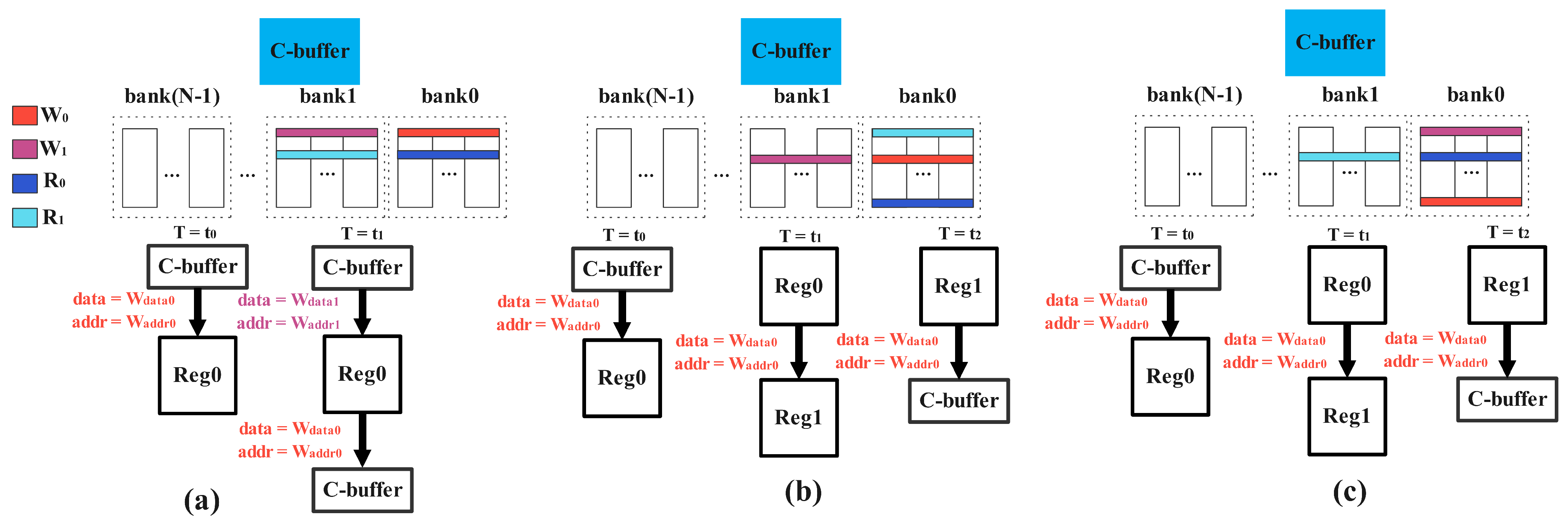
In Section 2.2 we can obviously see that, after using the SPM, the conflicts are inevitable. Then, according to the data mapping method after the memory access patterns expand by X times (while X is equal to 1, it is the same as the base idea), below we exemplify all the conflict situations, and analyze and explain these conflict forms. (Conflict: reading and writing occur simultaneously. In that group of banks, the read and write behaviors will come into conflict at this moment). Suppose that the read and write behaviors of the previous cycle () are and , respectively; the read and write behaviors of the current cycle () are and , respectively; and the read and write behaviors of the next cycle () are and , respectively. Here, we can arrange and combine all the conflicts, then divide them into three conflict situations:
(i) As Figure 6a shows, the conflict in this case attends to obtain the highest frequency of occurrence. In this case, , , and all conflict with , , and , respectively. The reading and writing of the previous cycle are exactly the same occurring in the same group of banks, because the data is stored in the skip group, so the and of the cycle also occur in the same group of banks, then in the next cycle and similarly occur in the same group of banks. (In this way, as long as the read and write are not blocked, the conflict will continue).
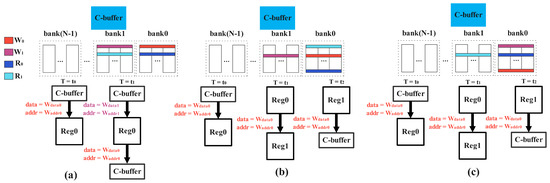
Figure 6.
The several type of conflicts of memory access.
(ii) According to our storage method, only when the last group of data stored in the C-buffer is stored in the first group of banks will there be no conflict between the read and write in the current cycle, and the conflict appears in the previous cycle (the C-buffer is used more than once in the matrix operation, the A matrix is fixed, and the B-buffer cannot store the entirety of matrix B at any time. Consequently, the B matrix will be involved. So, every time the block of the B matrix is switched, it will cause the reuse of the C matrix). We will discuss this conflict by 2 points: (1) as Figure 6b shows, at the current cycle, and occur in the first group of banks, while reads the last data in the C-buffer, and writes to a row in the middle of the first group of banks; at the current cycle continues to occur in the first group of banks, is written into the second group of banks, then the two signals in the next cycle is staggered; (2) as shown in Figure 6c, in the previous cycle, and occur in the first group of banks, while writes the last data in the C-buffer, reads a row in the middle of the first bank simultaneously, then continues to occur in the first bank, and reads the data in the second bank; the signals of reading and writing are staggered in the next cycle, which can lead to the conflict between writing and reading.
(iii) We can regard this case as the first case’s variant. This situation can only happen when the previous cycle acts on the last group of banks and acts on the first group of banks, then, at the current cycle, and both act on the first group of banks. In this way, at the next cycle, and also occur in the same group of banks (the second group). Like case 1, as long as the read and write are not blocked, the conflict will continue.
Based upon these several different situations, we will discuss the method of conflict resolution in the next section, which is also an important step in our SPM-based design.
4. ISPM
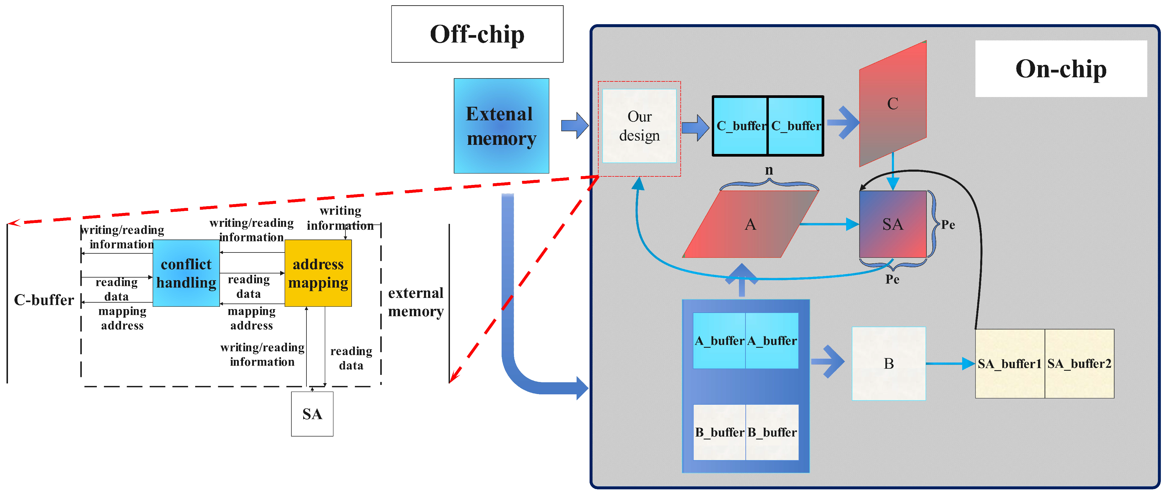
4.1. Architecture Overview
In this section, we give an overview of our architecture, as shown in Figure 7. On the basis of the architecture mentioned in Section 2.1, we design an on-chip module between the C-buffer and the external memory which connect to three module (external memory, C-buffer, and SA). Our module consists of the conflict-handling module and the address-mapping module. We consider both the external memory and SA’s writing data, address, and mask, as well as SA’s reading address and mask as the input of our module; the address is sent into the address-mapping module, which changes the address to the special address we want and this is finally sent into the C-buffer. Then, when SA needs to read the data in C-buffer, the reading address follows the same path. When the reading and writing signals are generated simultaneously, the conflict-handling module judges whether there is a conflict between the reading and writing signals, then the conflict-handling module sends the reading address and writing address (if it is without conflict) into the C-buffer. Finally, the read data from C-buffer are regarded as the output out of our module.
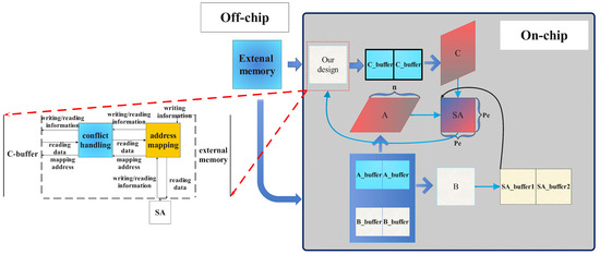
Figure 7.
The architecture overview.
4.2. Address-Mapping Module Design for the Base Idea
According to the analysis we conducted in Section 3.2, if the C-buffer from TPM to SPM must be changed, then it is necessary to ensure that, for each bank in the C-buffer, there can be no simultaneous reading and writing. At present, the depth of a bank is assumed to be z, a C-buffer capacity of L KB is unchanged, and a row in a bank stores 16 bits data (1024 bits), so a C-buffer has a total of banks arranged in order.
According to the address arrangement method mentioned in Section 3.2, we can use the formula to calculate the position of the data mapping in the external memory in the C-buffer. Specifically: given the initial address a that needs to be mapped, the initial judgment is whether n is a multiple of 16.
If it is a multiple of 16, we define a block can contain 1024 bit data, there are blocks in a row, so it is only necessary to calculate which row and column of a is among these blocks; that is,
where is the offset in bank of c, is the bank offset of c, and b is the converted address.
If it is not a multiple of 16, then a row has 16 blocks. If it is necessary to calculate the blocks of which row and column of a, then the value of n must be used to assist in reaching a judgment; that is,
and then the calculation formula is the same as in the case of 1.
However, for this address-calculation method, we need to use the variable m or n as the denominator of the division every time we convert the address, greatly increasing the time cost of the address conversion module, which is unacceptable to the hardware. Therefore, we have proposed a relatively hardware-friendly address-calculation method. The computation rules for the address from external memory to the C-buffer are as follows: because the data are read into the C-buffer as row-by-row data from the external memory, once the first address of the external memory is known, the address of that row is known, and then the first address of the second row can also be calculated based on the first address of the first row, and so on. The address of the external memory in the second row and first column should be added to the first address of the first row and first column. For example, each row in the external memory should first be divided into blocks with 16-bit data as the units. For the 0th row, its first address is , which corresponds to the bank offset in the C-buffer. The bank offset is , the first address of the next block is , the address corresponding to the bank offset in the C-buffer is , and the bank offset is . Similarly, for the next block in the same row, the calculation is performed according to the above formula. For the case of cross-line, once the first address of the previous line is known, the first address of the next line is equal to the first address of the previous line plus n, and the address in the C-buffer is (if is more then , then ).
4.3. Address-Mapping Module Design for Multiple Precision
Here, we discuss the implementation of the data storage in the C-buffer and the bank’s distribution when memory access patterns change. Due to the changing of C-buffer structure in Figure 5c, we use new expression of parameters instead of the expression in Section 4.2.
For half-precision or multiprecision data computation, in order to meet high-performance data throughput, we need to expand the C-buffer from the original group to X groups. Correspondingly, the number of banks in each group are changed from the original N (N is generally a multiple of 4), which becomes the current . At this time, the C-buffer structure is shown in Figure 5c. We arrange all N banks horizontally in a row and select every bank as a group to form a group of -bit-wide banks as a whole.
Then, we need to improve our address-mapping module. When the data is moved from the external memory to the on-chip C-buffer, due to memory access patterns requirements, the amount of data moved each time is X times the single memory access pattern, that is, the data moved each time is stored in the same row of a group of banks. Then, we must group the banks according to the data width required for this operation under different memory access patterns. For the same group of banks, we pass the same address into each bank of the group, and at the same time divide the data into blocks corresponding to the number of banks in the group, then we can see the N/X group of blocks, and in each group of blocks, there are X banks placed horizontally.
Specifically, for the first data block, we store the block into the first row of the first bank group, then as to the second block, we achieve a group jump when we map the address, this data block is stored in the first row of the second bank group. This method guarantees the alternativity of data storage.
We disassemble all the banks and arrange them horizontally, all the address lines of the banks are independent. We can regroup and connect the banks with different needs. It is assumed that a group’s memory access patterns of banks in the baseline single memory access patterns C-buffer is 1, and the memory access patterns to be expanded is X times of the baseline memory access patterns. At this time, the number of bank groups is . We numbered banks by 0 to , and the 0 to banks are a group, and so on. Every bank in the same group accesses the same write address, but each bank gets different input data, which is a split of bits of data. Different from the previous address mapping, since there is no reference for the input data, we set up a counter, CNT, to determine which group of banks the data should be written to. For each block of data written, CNT increases by one ( is also equal to the number of blocks of data in external memory). Then, we obtain a general address-mapping formula:
is the bank selection signal, and the is the address in the group of banks which is chosen, is the address of the data in external memory. According to the formula, we can perform address mapping processing for any kind of memory access patterns computation.
4.4. Conflict Handling Design
Here, we continue to use the expression described in Section 3.3, and we have carried out different designs according to the several conflict forms previously proposed.
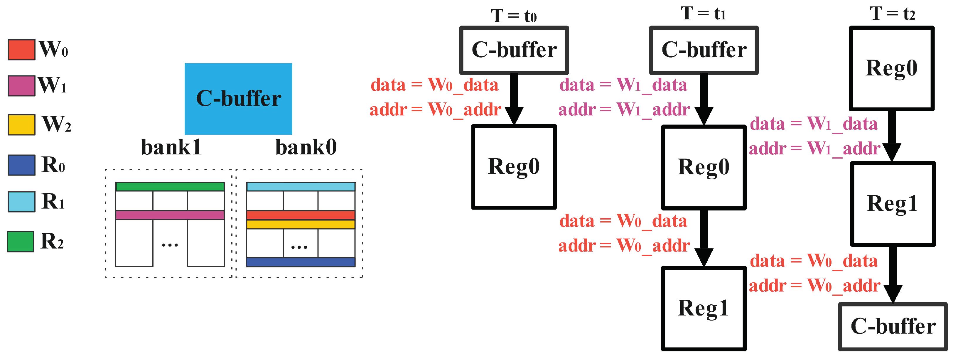
According to the idea of analysis of the case 1, we need to design a register to save the conflicting write data and address (because the priority of writing is lower than that of reading during design) to delay the writing of the data by one cycle, as shown in Figure 6a. In this way, a stable pipeline can be guaranteed, the of the previous cycle is written in the current cycle, and the data written in the current cycle are stored in the register to overwrite the data of the previous cycle.
However, according to the conflict forms in the second cases, when and conflict, the data and address information of are stored in the register. Because the next cycle does not cause a conflict, the Reg0 that saves the information is written to the first group of banks, but is also written to the first group of banks simultaneously. At this moment, there is a conflict between Reg0 and , so we need to add another register, Reg1, to store the information in Reg0 into Reg1, we delay by another one cycle, at the same time SA writes as usual, as shown in Figure 6b. Correspondingly, if acts on the first group of banks (at this moment, the last group of data which is stored in the first group of banks is read out corresponding to ), then the reading and writing conflict between Reg0 and occurs at this time, we use Reg1 to store Reg0’s information for one cycle to solve this problem, as shown in Figure 6c.
While the second case happens, we encounter a more difficult problem, when the number of bank groups is only 2 as shown in Figure 8, it causes the data in the register cannot be written to the C-buffer (if there is a read/write conflict on the first cycle and a conflict between Reg0 and on the second cycle, because there are only two groups of bank, acts on the first group of banks, which always leads to reading and writing conflicts. At this point, we need to change the way of conflict handling. In the first cycle, is stored in Reg0, and in the second cycle, is written into Reg1, at the same moment, is normally written into the C-buffer. In the third cycle, because of the conflict of and , we store into the Reg1, and in the Reg1 is written into the C-buffer to ensure the pipeline.

Figure 8.
The special conflict of memory access.
4.5. Limitations
In the process of hardware implementation, we have explored the scalability of this conflict-embracing design. The most important extension is whether the memory access patterns of the C-buffer is doubled or greater than the original. The memory method has an impact. However, there are also limitations with this design.
If the memory access patterns are expanded too wide, then the bank in each group may be only 1; under this address arrangement method we designed, there must be infinite conflicts that we can not handle, so if we want to ensure that the conflict can be tolerated, then the minimum number of banks must be greater than 1.
If the bank in each group is 1, a new problem arises—the bank depth must be reduced. According to the analysis and calculation of the data in Table 1, when the bank depth is reduced to half of the original, the space occupied by the memory bank is reduced, but the each bank’s area can not be reduced to half of the original. In other words, if the bank depth is reduced to half of the original, then the space occupied by the SPM to achieve the same effect is definitely larger. After comparison, although this has achieved the premise of conflict resolution conditions, the advantages of SPM-based design can be weakened. Intuitively, the space saving of SPM will become the original 130%. In general, the SPM banks and mapping method we have designed are extensible and can achieve the effect of reducing space spending, but the effect is not particularly clear. Furthermore, when the number of banks becomes very small, our SPM cannot continue to support it anymore, which is also the limitation of SPM.
5. Evaluation
In this section, we implement a systolic-array-based accelerator in verilog and emulate our designs with SPM and TPM on Palladium Z1. In addition, we also perform synthesis on SPM- and TPM-based designs to obtain the actual area overhead, respectively.
5.1. Metrics and Experimental Setting
Metrics: when it comes to the computing efficiency of SPM and TPM, we take the computing time (in microseconds) as the metric. With regards to the area, we evaluated the matrix calculations of SPM and TPM storage units with the same function through hardware.
We tested the time efficiency and accuracy verification of the systolic accelerator for computing matrices of different sizes through Palladium Z1. The frequency is 2 MHZ.
5.2. Experiments and Results
In this section, we conduct several different experiments to verify the feasibility and memory optimization of our proposed SPM.
Figure 9 shows the additional combinational and noncombinational logic area costs that our address-mapping module. We can observe that both combinational and noncombinational logic area costs increase a small scale in the whole C-buffer of less than 1%.
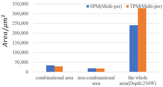
Figure 9.
The logic area costs for a multiprecision computation unit.
Table 3 illustrates the time taken for our SPM supporting multiple precision computation or not, TPM supporting multiple precision computation or not to compute the matrices of different sizes (here, we take the half-precision computation (it takes quadruple computing memory access patterns) as an example). We evaluate the effectiveness of computational efficiency from the total matrix computing time. From the figure, we observe that the time taken by our SPM-based design is quite close to the TPM, but with the multiple precision computing unit there is an clear time increase due to the banks choosing and some multiple precision computation design logic.
Table 3.
Computational Efficiency (µs).
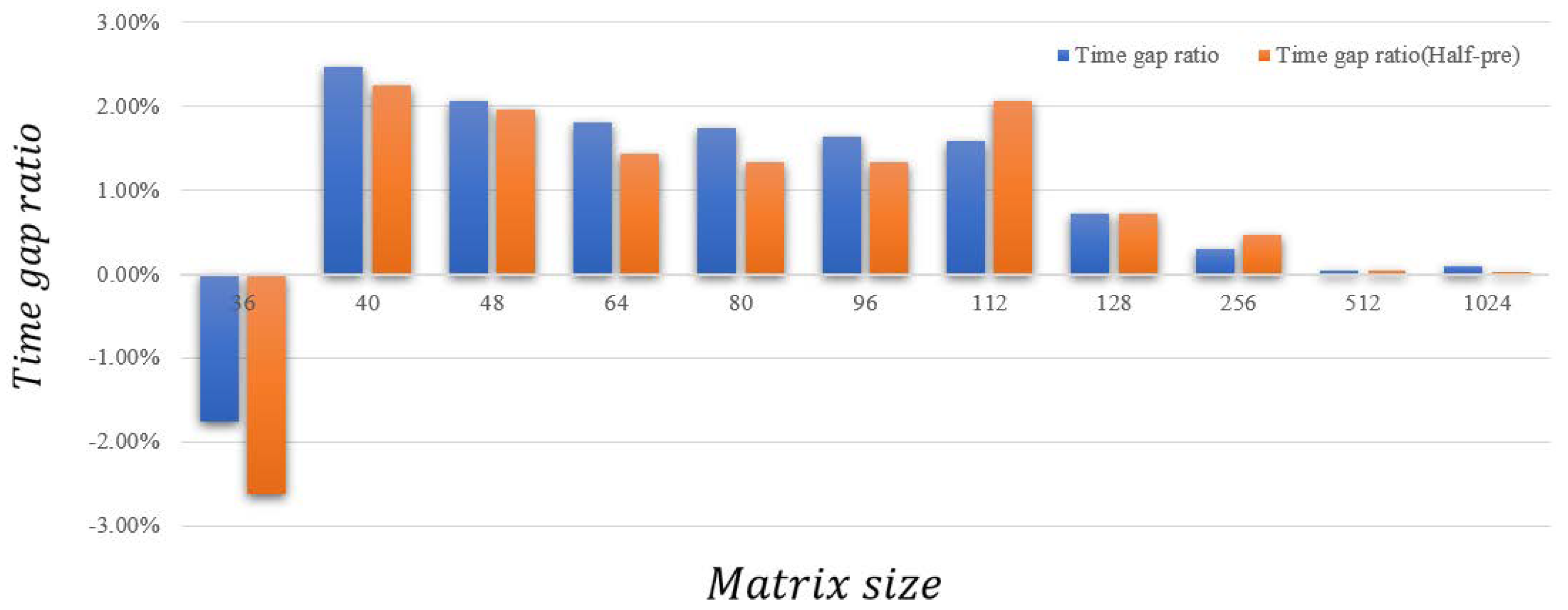
Note that as the size of the matrix increases, the time obtained for both, with multiprecision or not, increases exponentially. In Figure 10, we can observe that, compared to the TPM and TPM (multiprecision), our SPM-based design’s additional time cost grows very slowly. As the running time increases, the trend of the ratio is getting smaller, thereby getting closer to 0. Moreover, in engineering, the systolic array we have designed is not only intended to calculate a small-scale matrix multiplication, but the actual problem that needs to be calculated is larger. Therefore, when we actually use the SPM we have designed, the computational efficiency is very close to the TPM. Note that, when the matrix is small, the computation time of the Scal-BW design with quadrupling memory access patterns is really close to the basic design, which is mainly due to the removal time of the data being dominant. On the contrary, the computation time of the Scal-BW design is close to one quarter of the basic design. Simultaneously, the most important factor is that, after changing to our SPM-based design and after traversal calculation of different scale matrices, the accuracy of the matrix calculation results reached 100%. This also confirms the feasibility of the SPM we have designed and the comprehensiveness of conflict considerations.
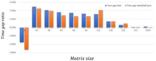
Figure 10.
The time gap ratio in different matrix size.
For SPM and TPM, supporting multiple precision computation or not, because we only modify the C-buffer module, the change of time is only reflected in this module. The additional time is the time consumed by address conversion and multiprecision computing arbitration. When designing the address conversion module of SPM, we took into account the time and space spending caused by multiplication and division to the hardware, and we optimized the calculation of the address to for multiplication and division, which is another reason that our SPM-based design is more efficient.
In Figure 10, we observe that there is an anomaly. When the size of the matrix is 36 × 36 × 36, the ratio appears to be lower than 0, and the test time increases. The anomaly is most likely caused by unevenness when the matrix is cut into 16 × 16 blocks, matching the size of the PE when the matrix size is very small. Take the 36 × 36 × 36 matrix and 40 × 40 × 40 matrix as examples. When calculating, the A-buffer is divided into two-scale matrices: 36 × 36 × 36:16 × 36 (two), 4 × 36 (one); 40 × 40 × 40:16 × 36 (two), and 8 × 36 (one). The calculation time for the first two matrices of the same size when they split is the same; only the third block is different. Compared to the 8 × 36 matrix, the 16 × 36 matrix has a higher occupancy rate in PE, so the calculation time increases instead.
Finally, our SPM-based design only takes a little time (which can be ignored) to complete matrix multiplication calculations while simultaneously maintaining computing accuracy.
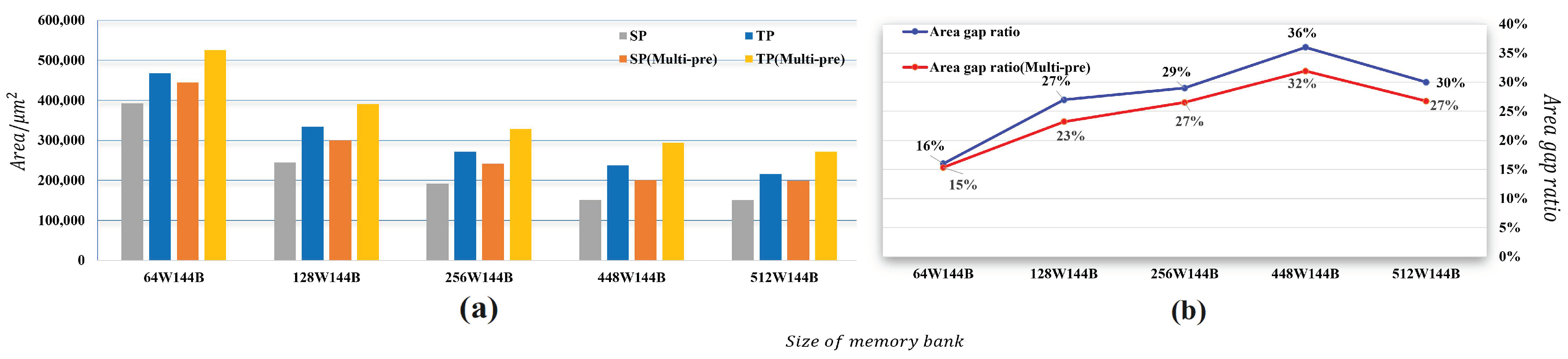
Figure 11 illustrates the comprehensive comparison of the area of SPM, TPM, SPM(Multi-pre), and TPM(Multi-pre). We evaluate the comparison of space spending between SPM and TPM by synthesizing both SPM and TPM on the hardware. From the figure, we can see that after synthesizing, the whole area of the C-buffer becomes very large, which includes many banks of the same depth and some addressing lines. With our SPM-based and multiprecision computation design, there is an additional address conversion module. We can observe that, as the depth of the bank becomes larger, the areas of both SPM and TPM become smaller. In other words, when we choose a bank unit, we should not choose a memory bank with a relatively small depth; using a relatively large bank unit can achieve a better space-saving effect.

Figure 11.
The difference between SPM and TPM at different depths: (a) the space cost; (b) the trend of the area ratio.
We can also conclude that, when it comes to the depth of around 448, the reduction in the area becomes negligible. Therefore, this also suggests that we should choose the upper limit of the depth of the basic storage unit.
As for a comparison between SPM and TPM, as we can see in Figure 11b, the area gap ratio is at least 16% without a multiprecision computation module. However, due to the multiprecision computation design, there is a large extra area spend (about 11%) compared with the SPM. Clearly, the area gap ratio of both designs apparently reduces. When the depth is 448, the area gap ratio, respectively, peaks at 36% and 31%. According to the data in the figure, we can easily observe that our SPM-based design achieves a strong result for optimizing space area.
As shown in Figure 11b, not only for basic SPM but also for SPM with multiprecision computation there is a trend that when the depth of the bank unit increases, their area gap between SPM and TPM also increases. Furthermore, when the depth increases to about 512, though their area gap still has a really great advantage, but this proportion is falling with the increasing of the bank’s depth. We can easily find that in Figure 11a the area becomes smaller with the depth of the bank unit increases; however, the substitute’s earning from SPM to TPM becomes less. When choosing the depth of the bank, we should consider both the limitation mentioned in Section 4.5 and area earning, so it is not necessary for us to use too deep banks.
Finally, we can see that our SPM-based design not only makes substantial saves for on-chip space resources, but it also maintains pulsating computing efficiency at the maximum level.
6. Related Work
Acceleration of the CNN for FPGA or ASIC [43] has gained the attention of researches in recent years. Most of them have focused on the filtering part, because that represents almost all of the computational workload of the CNN. Systolic implementations seem to be a natural fit, because they are very efficient at that filtering.
Some researchers [2,3,4] have proposed a convolution processing dataflow which reduces both the memory access and the on-chip buffer capacity for convolution operations. It almost focuses on how to handle the data flow to increase the utilization of the available resources on-chip. As for multiprecision computation, NVIDIA A100 Tensor Core GPU [36,37,38] has designed a set of components to support the multiple precision computation. To the best of our knowledge, We are the first to optimize the on-chip buffers from the prospect of memory device combined with multiprecision computation, rather than data reorganization or designing a specific dataflow.
7. Conclusions
This paper proposes an SPM-based access address arrangement method for multiprecision computation based on the data access characteristics of the systolic array structure accelerator, which can save the limited on-chip space area. Our SPM-based design solves the limitation of simultaneous reading and writing on-chip, while retaining the original TPM’s reading and writing behavior of the C-buffer. Our evaluation shows that our SPM-based design for multiprecision computation on the random-sized matrix achieves 100% accuracy for the calculation result, while the calculation efficiency is not reduced, compared with the SPM without multiprecision computation; the computation design increases the efficiency by four times. More importantly, compared with the other memory of the same size and depth, our SPM-based design saves about 30% and 25% on-chip space. However, when the memory becomes smaller, there will be fewer banks, which will mean that our SPM-based design will not work properly. We will improve this aspect in future work.
Author Contributions
Writing—original draft, R.Y. and J.S.; Writing—review & editing, R.Y., J.S., M.W., Y.C. and Y.L.; Figures, R.Y.; Study design, Y.L.; The other work, all authors contribute eqally. All authors have read and agreed to the published version of the manuscript.
Funding
This research was funded by National Nature Science Foundation of China under NSFC No.61802420 and 62002366.
Institutional Review Board Statement
Not applicable.
Informed Consent Statement
Not applicable.
Data Availability Statement
Not applicable.
Conflicts of Interest
The authors declare no conflict of interest.
References
- Exploration of Memory Access Optimization for FPGA-based 3D CNN Accelerator. In Proceedings of the 2020 Design, Automation & Test in Europe Conference & Exhibition (DATE), Grenoble, France, 9–13 March 2020.
- On-chip Memory Optimized CNN Accelerator with Efficient Partial-sum Accumulation. In Proceedings of the GLSVLSI ’20: Great Lakes Symposium on VLSI 2020, Virtual, 7–9 September 2020.
- Stoutchinin, A.; Conti, F.; Benini, L. Optimally scheduling cnn convolutions for efficient memory access. arXiv 2019, arXiv:1902.01492. [Google Scholar]
- Chang, X.; Pan, H.; Zhang, D.; Sun, Q.; Lin, W. A Memory-Optimized and Energy-Efficient CNN Acceleration Architecture Based on FPGA. In Proceedings of the 2019 IEEE 28th International Symposium on Industrial Electronics (ISIE), Vancouver, BC, Canada, 12–14 June 2019; IEEE: Piscataway, NJ, USA, 2019. [Google Scholar]
- Peemen, M.; Setio, A.; Mesman, B.; Corporaal, H. Memory-centric accelerator design for Convolutional Neural Networks. In Proceedings of the IEEE International Conference on Computer Design, Asheville, NC, USA, 6–9 October 2013; IEEE: Piscataway, NJ, USA, 2013. [Google Scholar]
- Alwani, M.; Chen, H.; Ferdman, M.; Milder, P. Fused-layer CNN accelerators. IEEE/ACM International Symposium on Microarchitecture. In Proceedings of the IEEE Computer Society, Pittsburgh, PA, USA, 11–13 July 2016; pp. 1–12. [Google Scholar]
- Jouppi, N.P.; Young, C.; Patil, N.; Patterson, D.; Agrawal, G.; Bajwa, R.; Bates, S.; Bhatia, S.; Boden, N.; Borchers, A.; et al. In-datacenter performance analysis of a tensor processing unit. Comput. Archit. News 2017, 45, 1–12. [Google Scholar] [CrossRef] [Green Version]
- Hennessy, J.L.; Patterson, D.A. Computer Architecture: A Quantitative Approach, 6th ed.; Elsevier: Amsterdam, The Netherlands, 2018. [Google Scholar]
- Ghose, S.; Boroumand, A.; Kim, J.S.; Gómez-Luna, J.; Mutlu, O. Processing-in-memory: A workload-driven perspective. IBM J. Res. Dev. 2019, 63, 3:1–3:19. [Google Scholar] [CrossRef]
- Liu, J.; Zhao, H.; Ogleari, M.A.; Li, D.; Zhao, J. Processing-in-Memory for Energy-Efficient Neural Network Training: A Heterogeneous Approach. In Proceedings of the 2018 51st Annual IEEE/ACM International Symposium on Microarchitecture (MICRO), Fukuoka, Japan, 20–24 October 2018; pp. 655–668. [Google Scholar] [CrossRef]
- Gokhale, M.; Holmes, B.; Iobst, K. Processing in memory: The Terasys massively parallel PIM array. Computer 1995, 28, 23–31. [Google Scholar] [CrossRef]
- Chi, P.; Li, S.; Xu, C.; Zhang, T.; Zhao, J.; Liu, Y.; Xie, Y. PRIME: A Novel Processing-in-Memory Architecture for Neural Network Computation in ReRAM-Based Main Memory. In Proceedings of the 2016 ACM/IEEE 43rd Annual International Symposium on Computer Architecture (ISCA), Seoul, Korea, 18–22 June 2016; pp. 27–39. [Google Scholar] [CrossRef]
- Abdelfattah, A.; Tomov, S.; Dongarra, J. Towards Half-Precision Computation for Complex Matrices: A Case Study for Mixed Precision Solvers on GPUs. In Proceedings of the 2019 IEEE/ACM 10th Workshop on Latest Advances in Scalable Algorithms for Large-Scale Systems (ScalA), Denver, CO, USA, 18 November 2019; ACM: New York, NY, USA, 2019. [Google Scholar]
- Ye, D.; Kapre, N. MixFX-SCORE: Heterogeneous Fixed-Point Compilation of Dataflow Computations. In Proceedings of the IEEE International Symposium on Field-Programmable Custom Computing Machines, Boston, MA, USA, 11–13 May 2014; IEEE Computer Society: Piscataway, NJ, USA, 2014. [Google Scholar]
- Burtscher, M.; Ganusov, I.; Jackson, S.J.; Ke, J.; Ratanaworabhan, P.; Sam, N.B. The vpc trace-compression algorithms. IEEE Trans. Comput. 2005, 54, 1329–1344. [Google Scholar] [CrossRef]
- YYang, E.H.; Kieffer, J.C. Efficient universal lossless data compression algorithms based on a greedy sequential grammar transform–part one: Without context models. IEEE Trans. Inf. Theory 2000, 46, 755–777. [Google Scholar] [CrossRef]
- Guay, M.; Burns, D.J. A comparison of extremum seeking algorithms applied to vapor compression system optimization. In Proceedings of the American Control Conference, Portland, ON, USA, 4–6 June 2014; IEEE: Piscataway, NJ, USA, 2014. [Google Scholar]
- Reichel, J.; Nadenau, M.J. How to measure arithmetic complexity of compression algorithms: A simple solution. In Proceedings of the IEEE International Conference on Multimedia & Expo, New York, NY, USA, 30 July–2 August 2000; IEEE: Piscataway, NJ, USA, 2000. [Google Scholar]
- Yokoo, H. Improved variations relating the ziv-lempel and welch-type algorithms for sequential data compression. IEEE Trans. Inf. Theory 2006, 38, 73–81. [Google Scholar] [CrossRef]
- Samajdar, A.; Zhu, Y.; Whatmough, P.; Mattina, M.; Krishna, T. Scale-sim: Systolic cnn accelerator simulator. arXiv 2018, arXiv:1811.02883. [Google Scholar]
- Shen, J.; Ren, H.; Zhang, Z.; Wu, J.; Jiang, Z. A High-Performance Systolic Array Accelerator Dedicated for CNN. In Proceedings of the 2019 IEEE 19th International Conference on Communication Technology (ICCT), Xi’an, China, 16–19 October 2019; IEEE: Piscataway, NJ, USA, 2019. [Google Scholar]
- Kung, H.T.; Leiserson, C.E. Systolic arrays (for VLSI). In Sparse Matrix Proceedings 1978; Society for Industrial and Applied Mathematics: Philadelphia, PA, USA, 1979; pp. 256–282. [Google Scholar]
- Law, K.H. Systolic arrays for finite element analysis. Comput. Struct. 1985, 20, 55–65. [Google Scholar] [CrossRef]
- Lacey, G.; Taylor, G.W.; Areibi, S. Deep learning on fpgas: Past, present, and future. arXiv 2016, arXiv:1602.04283. [Google Scholar]
- Chen, Y.; Emer, J.; Sze, V. Eyeriss: A Spatial Architecture for Energy-Efficient Dataflow for Convolutional Neural Networks. In Proceedings of the 2016 ACM/IEEE 43rd Annual International Symposium on Computer Architecture (ISCA), Seoul, Korea, 18–22 June 2016; pp. 367–379. [Google Scholar] [CrossRef] [Green Version]
- Genc, H.; Kim, S.; Amid, A.; Haj-Ali, A.; Iyer, V.; Prakash, P.; Shao, Y.S. Gemmini: Enabling Systematic Deep-Learning Architecture Evaluation via Full-Stack Integration. In Proceedings of the 2021 58th ACM/IEEE Design Automation Conference (DAC), San Francisco, CA, USA, 13 November 2021; pp. 769–774. [Google Scholar] [CrossRef]
- Pop, S.; Sjodin, J.; Jagasia, H. Minimizing Memory Access Conflicts of Process Communication Channels. U.S. Patent 12/212,370, 18 March 2010. [Google Scholar]
- Kasagi, A.; Nakano, K.; Ito, Y. An Implementation of Conflict-Free Offline Permutation on the GPU. In Proceedings of the 2012 Third International Conference on Networking and Computing, Portland, OR, USA, 13–17 June 2013; IEEE: Piscataway, NJ, USA, 2013. [Google Scholar]
- Ou, Y.; Feng, Y.; Li, W.; Ye, X.; Wang, D.; Fan, D. Optimum Research on Inner-Inst Memory Access Conflict for Dataflow Architecture. J. Comput. Res. Dev. 2019, 56, 2720. [Google Scholar]
- Feng, L.; Ahn, H.; Beard, S.R.; Oh, T.; August, D.I. DynaSpAM: Dynamic spatial architecture mapping using Out of Order instruction schedules. In Proceedings of the 2015 ACM/IEEE 42nd Annual International Symposium on Computer Architecture (ISCA), Portland, OR, USA, 13–17 June 2015; IEEE: Piscataway, NJ, USA, 2015. [Google Scholar]
- Chen, Y.H.; Emer, J.; Sze, V. Eyeriss: A spatial architecture for energy-efficient dataflow for convolutional neural networks. Comput. Archit. News 2016, 44, 367–379. [Google Scholar] [CrossRef]
- Bao, W.; Jiang, J.; Fu, Y.; Sun, Q. A reconfigurable macro-pipelined systolic accelerator architecture. In Proceedings of the International Conference on Field-Programmable Technology, Seoul, Korea, 10–12 December 2012; IEEE: Piscataway, NJ, USA, 2012. [Google Scholar]
- Ito, M.; Ohara, M. A power-efficient FPGA accelerator: Systolic array with cache-coherent interface for pair-HMM algorithm. In Proceedings of the 2016 IEEE Symposium in Low-Power and High-Speed Chips (COOL CHIPS XIX), Yokohama, Japan, 20–22 April 2016; IEEE: Piscataway, NJ, USA, 2016. [Google Scholar]
- Pazienti, F. A systolic array for neural network implementation. In Proceedings of the Electrotechnical Conference, Cairo, Egypt, 7–9 May 2002; IEEE: Piscataway, NJ, USA, 2002. [Google Scholar]
- Cignoni, P.; Montani, C.; Rocchini, C.; Scopigno, R. External memory management and simplification of huge meshes. IEEE Trans. Vis. Comput. Graph. 2003, 9, 525–537. [Google Scholar] [CrossRef] [Green Version]
- Choquette, J.; Gandhi, W.; Giroux, O.; Stam, N.; Krashinsky, R. NVIDIA A100 Tensor Core GPU: Performance and Innovation. IEEE Micro 2021, 41, 29–35. [Google Scholar] [CrossRef]
- Svedin, M.; Chien, S.W.; Chikafa, G.; Jansson, N.; Podobas, A. Benchmarking the Nvidia GPU Lineage: From Early K80 to Modern A100 with Asynchronous Memory Transfers. In Proceedings of the 11th International Symposium on Highly Efficient Accelerators and Reconfigurable Technologies, Virtual, 21–23 June 2021. [Google Scholar]
- Lyakh, D.I. An efficient tensor transpose algorithm for multicore CPU, Intel Xeon Phi, and NVidia Tesla GPU. Comput. Phys. Commun. 2015, 189, 84–91. [Google Scholar] [CrossRef] [Green Version]
- Jang, B.; Schaa, D.; Mistry, P.; Kaeli, D. Exploiting Memory Access Patterns to Improve Memory Performance in Data-Parallel Architectures. IEEE Trans. Parallel Distrib. Syst. 2011, 22, 105–118. [Google Scholar] [CrossRef]
- Weinberg, J.; McCracken, M.O.; Strohmaier, E.; Snavely, A. Quantifying Locality In The Memory Access Patterns of HPC Applications. In Proceedings of the Supercomputing, ACM/IEEE Sc Conference, Online, 12–15 November 2005; ACM: New York, NY, USA, 2005. [Google Scholar]
- Lorenzo, O.G.; Lorenzo, J.A.; Cabaleiro, J.C.; Heras, D.B.; Suárez, M.; Pichel, J.C. A Study of Memory Access Patterns in Irregular Parallel Codes Using Hardware Counter-Based Tools. In Proceedings of the International Conference on Parallel and Distributed Processing Techniques and Applications (PDPTA), Las Vegas, NV, USA, 16–19 July 2012. [Google Scholar]
- Arimilli, R.K.; O’Connell, F.P.; Shafi, H.; Williams, D.E.; Zhang, L. Data Processing System and Method for Reducing Cache Pollution by Write Stream Memory Access Patterns. U.S. Patent 20080046736 A1, 21 February 2008. [Google Scholar]
- Caffarena, G.; Pedreira, C.; Carreras, C.; Bojanic, S.; Nieto-Taladriz, O. Fpga acceleration for dna sequence alignment. J. Circuits Syst. Comput. 2008, 16, 245–266. [Google Scholar] [CrossRef]


Publisher’s Note: MDPI stays neutral with regard to jurisdictional claims in published maps and institutional affiliations. |
© 2022 by the authors. Licensee MDPI, Basel, Switzerland. This article is an open access article distributed under the terms and conditions of the Creative Commons Attribution (CC BY) license (https://creativecommons.org/licenses/by/4.0/).