Abstract
A sustainable computing scenario demands more energy-efficient processors. Neuromorphic systems mimic biological functions by employing spiking neural networks for achieving brain-like efficiency, speed, adaptability, and intelligence. Current trends in neuromorphic technologies address the challenges of investigating novel materials, systems, and architectures for enabling high-integration and extreme low-power brain-inspired computing. This review collects the most recent trends in exploiting the physical properties of nonvolatile memory technologies for implementing efficient in-memory and in-device computing with spike-based neuromorphic architectures.
1. Introduction
Neuromorphic computing has become an attractive candidate for emerging computing platforms for both large-scale systems and edge nodes. Neuromorphic computing provides design principles and ideas borrowed by natural neural systems, and it has the potential to drive the development of a more distributed, scalable, and efficient computing paradigm. Historically, the term neuromorphic computing was coined in the late 1980s to describe analog computing systems (hardware) that mimic the brain’s architecture [1]. Initially, the primary goal of neuromorphic computing was to emulate the physical properties of neurons and synapses with the physics of analog complementary-metal-oxide-semiconductor (CMOS) electronics to build computing architectures while understanding and reproducing the efficiency of neural computing systems. Today, neuromorphic computing addresses a broader range of computing systems based on digital, mixed-signal (analog/digital) CMOS electronics, photonics, and novel emerging technologies elements. Yet, in all neuromorphic systems, the aim is to build architectures that can support the execution of Spiking Neural Networks (SNNs) for achieving efficient neural information processing. SNNs today represent the third and more bio-inspired generation of neural networks [2]. Over the past decades, there has been a significant amount of progress made in neuromorphic computing, both on the software (e.g., application and algorithm [3,4,5,6,7,8,9,10,11,12]) and hardware (e.g., architecture and technology [13,14,15,16,17]) fronts. These architectures and algorithms differ from conventional computing paradigms in their memory and communication structures and computational properties. While traditional von Neumann architectures have one or more central processing units physically separated from the main memory, neuromorphic architectures exploit the co-localization of memory and compute, near and in-memory computation [18]. Simultaneously to the tremendous progress in devising novel neuromorphic computing architectures, there has been many recent works that address how to map and compile (trained) SNNs models for efficient execution in neuromorphic hardware [19,20,21,22,23,24,25,26,27,28,29,30,31].
This work focuses on the hardware and architectures that support efficient spiking neural networks with nonvolative memory (NVM) devices. Examples of architecture that support spiking neural networks with traditional CMOS hardware alone are SpiNNaker [32], TrueNorth [33], Loihi [34], Brain [35], ODIN [36], NeuroGrid [37], BrainScaleS [38], Tianji [39], PRIME [40], and DYNAPs [41], among others. Although these computing architectures provide significant scalability and energy efficiency when executing SNNs, they all use CMOS technologies for neuron circuits and Static Random-Access Memories (SRAMs) for synapses. The use of SRAM synapses greatly impacts the device area. It is responsible for a considerable portion of the power consumption, mainly caused by data movement, and static leakage power. For this reason, recently, there has been an increased interest in nonvolatile memory (NVM) technologies for neuromorphic computing [16,42,43,44,45,46,47,48,49], beyond their potential as DRAM replacement or as hybrid memory in shared memory systems [50,51,52,53,54]. Nonvolatile devices provide a broad range of excellent properties for neuromorphic architectures, including memory retention, analog behavior, high integration density, increased read/program speed, high energy efficiency, and programming voltages compatible with CMOS electronics. In particular, the scaling of dense NVMs crossbars arrays to few nanometers is crucial for building large-scale systems that can mimic the high degree of connectivity present in brains, in which each neuron is connected, on average, to 10,000 other neurons. In addition, NVMs have physical properties that can be used to mimic the physical properties of neurons and synapses, offering a path towards the emulation of natural neural information in highly dense and low-power neural processing architectures. However, several challenges need to be addressed to achieve robust neural computation with these elements. These challenges include the need for peripheral circuitry for operating the NVMs, calibration procedures, and the need for novel models of computations implemented in massively parallel networks of low-power neurons and synapses. In addition, there is a need to understand how to overcome the inherent limitations of NVMs devices as their limited reliability, limited dynamic range, significant programming energy, and nonidealities such as nonlinear operations, and drift over time. However, since biology manages to self-adapt and construct highly functional neural networks from stochastic and inhomogenous neurons and synapses, there is the ambition to understand how to best exploit online learning, homeostatic, and self-healing mechanisms to adapt and compensate for internal and external deviations. Such mechanisms could potentially enforce robust computations despite the presence of defective and variable devices [55,56,57,58]. Our contributions in this paper are as follows:
- A complete overview of device physics, working, and drawbacks of the NVM devices.
- We discuss nonvolatile memory integration in hybrid CMOS and NVMs neuromorphic architectures with in-memory computing abilities, including large-scale and edge computing systems.
- We discuss relevant and up-to-date publications on SNN computing architectures with NVM devices.
- We provide a roadmap for the coming years, providing outlooks on the new applications in which NVMs are critical enablers.
In Section 2, we provide explanations for the basic operations of several NVM devices and their operational properties, and we describe how they can be integrated into neuromorphic architectures. This is followed by Section 3, where we look at some of the emerging materials that can be used in composition with existing prototype NVMs for better performance. In Section 4, we provide examples of the most recent large-scale spike-based neuromorphic architectures in which NVMs have been integrated. In Section 5, we provide examples of spike-based neuromorphic edge architectures in which NVMs play a crucial role in enabling emerging application scenarios as biomedical signal processing. Finally, in the conclusions and discussion, Section 6, we compare several properties of the NVMs, and we provide a short outlook highlighting the challenges that still need to be solved and the opportunities that lie ahead in the quest for a more efficient, bio-inspired way for artificial systems to perform computation in emerging applications.
2. Trends in Nonvolatile Memory-Based SNN Architectures
Nonvolatile memories can be divided into prototype and emerging classes. The pototype class is made up of all the established device structures that have been making their way from academia to industry. Figure 1 shows the state-of-the-art operation parameters of different NVMs devices, which we discuss in Section 2.1, Section 2.2, Section 2.3, Section 2.4 and Section 2.5. In Section 3, we discuss the emerging materials for NVM devices.
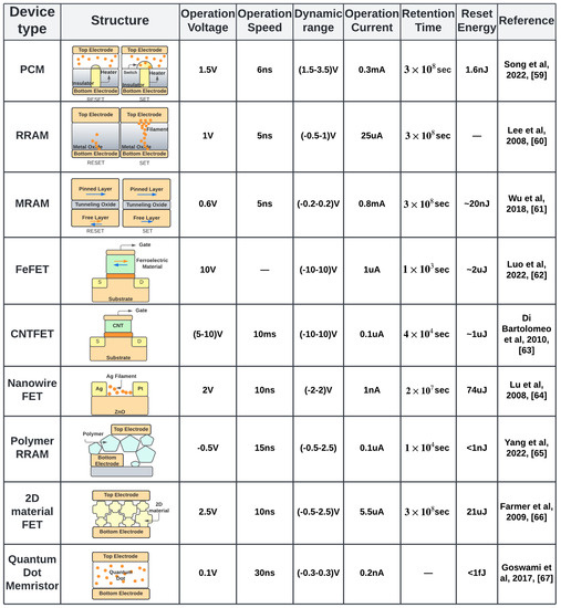
Figure 1.
Device-level operation parameters of different NVMs where operation voltage, speed and current are reported for the ON state of the device while dynamic range is the (OFF–ON) voltage range [59,60,61,62,63,64,65,66,67].
2.1. Phase-Change Memory
Phase-Change Memories (PCM) are the most advanced and front runners in the field of nonvolatile memories. They are part of a Chalcogenide family (primarily Group VI elements) based two-dimensional material sandwiched between two metal electrodes, and a resistive electrode referred to as heater [68,69] (Figure 1). Most commonly studied ones are the Ge-Sb-Te (GST) class of materials [70,71,72]. The presence of two distinct solid-state phases, i.e., crystalline and amorphous, with contrasting electrical and optical properties, makes them an attractive choice. The dynamic switching between amorphous-to-crystalline phases of the material in the presence of electrical pulses is used to model neuron’s integration and firing behavior. When the PCM material is in the amorphous phase, it has high resistance (i.e., the high-resistance state HRS). The PCM crystallizes by applying medium voltage electric pulses. This represents the device’s SET operation, which incrementally increases the amorphous layer thickness and is used to model the temporal integration of membrane potential in a neuron implementation. When the PCM reaches a full crystallization state, the device presents a low resistance (i.e., low-resistance state LRS). The LRS is used to model the neuron’s threshold. Upon reaching it, the neuron fires (i.e., the device is in the LRS). Under high voltage short electric pulse, there is a generation of high current densities at the interface of the heater and the PCM material creating a Joule heating effect. This is used to perform the RESET operation after the emission of an action potential (i.e., a spike). The Joule heating is responsible for switching the crystalline phase back to the amorphous phase. The RESET is an abrupt process of melting and quenching followed by rapid cooling of the material. Figure 2a illustrates a chalcogenide semiconductor alloy that was used to build a PCM cell. Figure 2b shows the different current values needed to program and read a PCM device. Therefore, depending on whether a PCM device in a crossbar is programmed to SET state, RESET state, or one of the intermediate states, different amount of current will be required to program and read.
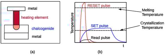
Figure 2.
(a) A phase change memory (PCM) cell and (b) temperature needed to SET, RESET, and read.
To read the PCM state, we applied a low voltage in the OFF region of the device, which, in turn, produces a readout current, as shown in Figure 3. The switching speed determines the write speed from the amorphous to the crystalline phase, and the SET operation determines the operating step speed of this device. Recent studies show that PCM devices have a write speed to the order of 100 ns, performing better than Flash memory at lower voltages [73]. One of the unique advantages of PCM, unlike Flash memory, is the possibility to overwrite memory without the need of erasing. Nevertheless, the RESET of PCM requires high write power due to the heat-dependent switching mechanism. Since programming in the SET state is incremental with repetitive pulses slowly increasing the mushroom type switching volume, PCM can also be used to represent multiple intermediate states between fully-crystalline and fully-amorphous [74]. This gives the capability to store multiple bits in a cell encoded in intermediate states. In [75], a triple-level PCM array of 64 k cells is demonstrated by Milos et al. on a 90 nm CMOS baseline chip with permutation encoding to shift the threshold of each level considering the shift in drift resistance. These devices are popularly known as PCRAM, Lance-type, or Ovonic unified memory.
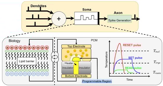
Figure 3.
Spiking neuron with PCM. The physical properties of PCM can be used to emulate the dynamics of biological neurons. In this example, a PCM device is used to model current integration and the nonlinear neuron spiking behavior [76].
Considering their high ON/OFF ratio, PCMs can also be employed as synapses with inexpensive and high-speed information transfer. In [77], Kuzum et al. use repetitive pulses to achieve a PCM-based synapse. Here, each of the top and bottom electrodes are sent presynaptic and postsynaptic pulses, respectively. The difference in the pulse potential is applied to the memristor whose resistance stores the synaptic weight. When the presynaptic electrode spikes later than the postsynaptic electrode, the potential difference leads to the amorphization of the device. This mechanism has a perfect resemblance with the spike-timing dependent plasticity (STDP) learning rule [78].
A two-PCM approach is proposed to implement both long-term potentiate (LTP) and long-term depression (LTD) modes of STDP [79]. However, controlling the abrupt transition in the RESET process on multiple devices simultaneously is difficult to achieve as it requires extra circuitry. Kuzum et al., in [80], use pulses of varying amplitudes to program SET and RESET using a single PCM cell. In this work, both potentiate and depression branches of the STDP learning are implemented per synapse. In [81], Yi et al. show that configuring pulses at different time windows can be utilized to break down STDP into its four different variants.
The integration of PCRAM in a crossbar array facilitates large-scale storage and in-memory computing. However, writing to PCM cells in a crossbar array can incur programming current sneaking to nearby cells producing undesirable results [82,83]. Selector devices can avoid sneak path currents. The resulting crossbar can be in 1T-1R, i.e., one transistor one memristor, or 1S-1R, i.e., one selector diode and one memristor arrangement. In [84], Eryilmaz et al. demonstrate STDP for simple patterns with a 10 × 10 crossbar with 1T-1R PCM cells. However, in-situ training on NVM hardware has lower accuracy than software. In [85], Ambrogio et al. demonstrate a hardware-software approach of neural network implementation for complex image recognition. The 3T-1C cell array of hardware with supervised learning schemes implemented in software has similar accuracy as software-based schemes while being more energy efficient and fast.
At the system level, the high current requirement of PCM devices leads to thermal [83] and reliability concerns [86,87]. In [88], Balaji et al. show that in order to generate currents in a PCM crossbar, the charge pumps need to be operated at an elevated voltage, which accelerates the aging in its transistors. In [89], Song et al. show that high aging in the CMOS device of a neuron in a PCM crossbar can lead to a lower lifetime. This is due to the high voltage operations needed to generate the SET and RESET currents in the PCM crossbar. Finally, in [90], Song et al. show that prolonged execution of machine learning workloads on a PCM crossbar can lead to timing failures due to circuit degradation.
Even though a crossbar architecture is more compatible for implementing spiking neural networks, every PCM device in a crossbar is in series with a selector device that generates the RESET current. Thus, downscaling of PCRAM and the selector device must ensure that the selector can produce enough current to RESET the PCRAM cell. This scaling limitation of PCRAM can be solved by shrinking the heater-PCM interface region [91] or cell structures with advanced device engineering [92]. Several alternative selector devices such as BJT, diodes, and Schottky diodes are used to alleviate the potential problem of producing adequate heating resistance that instigates the Joule heating. One such device is mixed ionic-electronic conduction (MIEC), which is used for 3D integration [93].
Another challenge with PCM devices is the change in drift resistance overtime when the device is in the high-resistance state (HRS). PCM drifts occur due to structural relaxation [94] or mechanical relaxation [95] after programming the resistance of the memristor. Downscaling of PCM also leads to a challenge in programming a PCM in one of the intermediate levels. Finally, the endurance of PCM is around 10 cycles, which is not compatible with many learning and inference applications [82,96]. Clearly, there is a need for more device-oriented research to overcome the technological limitations and evaluate their system-level impact in order to make PCM-based neuromorphic computing successful.
2.2. Resistive Ram
Much like PCM, Resistive Random-Access Memories (RRAM) have been explored in depth by many since the discovery of variable resistance anodic oxide materials [97,98]. The dynamic of RRAM is governed by the switching of a metal–insulator–metal (MIM) structure where the insulator can be an oxide or an electrolyte. The switching could be caused by thermo-chemical effects, which induce unipolar structures, or nano-ionic redox effect induced bipolar structures. Bipolar devices show conducting and insulating behavior for opposite bias applied on the two metal electrodes. Usually, both electrodes are active. However, in the case of an electrolyte insulator, one of the electrodes remains inert. Figure 4 shows an RRAM cell, where the insulating film () is placed between two conducting electrodes forming the MIM structure. The left subfigure shows the formation of LRS states using the conducting filament. The right subfigure shows the depletion of the filament on application of a negative voltage to the top metal. This represents the HRS state.
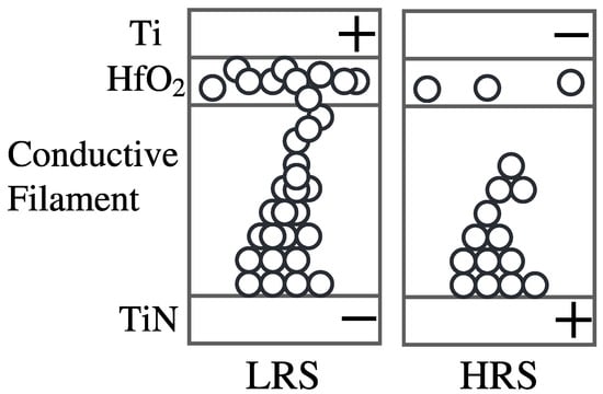
Figure 4.
Operation of an RRAM cell.
Consider an RRAM cell that is initially in the high-resistance state (HRS). Then, with the application of high forming voltage, the RRAM cell switches from HRS to the low-resistance State (LRS). This is the SET operation of RRAM. Unlike PCM, RRAM works as an integrated unit when connected in parallel with a capacitor in an RC circuit. This forms the basis for the implementation of a leaky-integrate-and-fire (LIF) neuron [99]. For a leaky-integrate-and-fire (LIF) neuron, the membrane potential can be modeled as the concentration of oxygen vacancies. During the voltage sweep measurement of MIM structures, the dielectric breakdown leads to a jump in the current, which could be converted into an analog spike output. Several switching mechanisms have been discovered in recent years, some of which are discussed below.
Filamentary RRAMs are composed of those oxides that form a chain of defects that can act as a filament. These defects are formed due to thermal redox reactions between the metal and oxide interface. Forming the conductive oxide path in the presence of a high electric field displaces the oxygen atoms from its lattice, creating vacancies. This is called the SET operation. The RESET phenomenon occurs when ions diffuse from the anode to balance the oxygen concentration and rupture the filament. In [100], Preziso et al. experimentally demonstrate STDP implementation on memristors which are self-tuned to the presynaptic and postsynaptic pulses independent of their initial synaptic weights. In addition, it is possible to obtain multilevel resistance states by varying the programming voltage amplitudes during the pulse cycling, thus increasing or decreasing the conductance in a cycle-to-cycle manner [101]. Interestingly, in [102], Valentian et al. show that filament devices are compatible with CMOS integration.
Nonfilamentary RRAM, on the other hand, are devices in which defects migrate to the Schottky barrier of the metal/oxide interface. Defects change the functionality of the material with additional defect energy bands in the energy diagram of the device, resulting in resistance change. In [103], Hansen et al. demonstrate a double barrier memristive device with oxide tunnel barrier and Schottky barrier. They show that nonfilamentary-based switching has improved retention compared to filamentary devices. In [104], Yang et al. alter the frequency to transition from Short-Term Plasticity (STP) to Long-Term Plasticity (LTP) in the inorganic based synapse. When the pulse width is reduced to achieve a higher frequency, the memorization strength of the nonvolatile memory increases. Implementation of STP and LTP with a single device indicates the resemblance of the artificial nanodevice to a biological synapse.
Conductive-Bridge RRAM (CBRAM) is similar to filamentary RRAM [105]. The filament formation occurs in an electrolyte medium due to electrochemical reactions. With one active and one inert metal electrode, the bias of the anode determines the movement of metal ions (like Cu or Ag). When a positive bias is applied to the anode, metal ions start drifting to the cathode, leading to a reduction (oxidation) at the anode (cathode). Accumulation of metal ions at the cathode forms a filament incrementally. An opposite bias breaks the growth of the material. In [106], Fackenthal et al. demonstrate a three-layer Cu-based chip with a 16 GB array of memory cells divided into an architecture composed of eight tiles for commercial use. In [107], Wijesinghe et al. implement the functionality of a deep stochastic spiking neural network (SNN) on a 32 × 32 crossbar with CBRAM memristors. The proposed design is compatible with any ANN network producing similar accuracy for less energy consumption.
RRAM’s read disturbance issues create system-level challenges for the successful deployment of RRAM in neuromorphic architectures [108]. The authors show that if the read disturbances are not incorporated during the mapping of deep learning models, the correct operations of the device over its lifetime can significantly be reduced [109,110]. To address this, model parameters need to be reprogrammed periodically, which leads to high system overhead [111]. Like PCM, RRAM also suffers from resistance drift, which is also recently studied [112]. Recently, authors reported the latency overhead of RRAM’s multilevel cell operation and its system-level implications [112].
Another technological challenge of RRAM is represented by the interactions at the metal-electrolyte interface, which reduce the reliability of CBRAM [113]. There also exists a tradeoff between programming speed and retention in nonfilamentary RRAM. Higher switching speed is achieved with a low energy barrier, but this might limit the operating range to a certain time domain [114]. Material engineering to use thinner insulator layers can address this issue. However, filamentary RRAM shows significant variability due to considerably short switching time [115]. Furthermore, device and material engineering that provides better control over the conductance update of the device is required.
2.3. Magnetoresistive Ram
Resistive and phase change memory cells suffer from degradation over time and limited endurance cycles. Magnetoresistive RAM (MRAM) alleviates this issue by providing almost unlimited endurance with a fast switching mechanism [116]. Instead of exploiting device physics as in PCM and RRAM, MRAMs are the class of memristors that exploits memristive properties, e.g., via a change in the magnetic state of the device, also known as magnetoresistance. The magnetoresistance property is very similar to the operation of a hard disk drive. Since magnetic polarization is independent of the power supply, it behaves as nonvolatile memory. Switching in MRAM is governed by the spin dynamics of electrons, and it does not involve any movement of subatomic particles making it less subjected to wear-out.
Magnetic Tunnel Junction (MTJ) is the first device to utilize electron spin as a memory storage variable [117]. MTJ comprises two ferromagnetic nanomagnets with a dielectric layer in the middle. This composition is the same for all other devices discussed below. However, in MTJ, one nanomagnet has fixed magnetic polarization, and the other is free. Current induced switching between parallel and anti-parallel states transfers the spin to nanomagnets [43].
In Spin Transfer Torque (STT) MRAM [118,119], the magnetization changes due to torque transfer from incoming electrons. Continuous application of input spikes is integrated to switch the polarization of magnetizing material. In [120], Rezeszut et al. usea multi-bit STT-MRAM cell as a synapse to recognize the MNIST database. The I-V curve was tuned to simulate seven serially connected MTJs to represent 8-bit data. The proposed design requires no additional hardware with programmable MTJ multi-cells comparing the input to enable positive or negative weights. A select transistor could also be used for the same. The neuron circuit combines MTJ synapse, differential amplifiers, and a sigmoid function generator.
Recently, Spin-Orbit Torque (SOT) MRAM has gained interest due to its high spin injection efficiency [121]. SOT-MRAM switches due to domain wall movement by an orthogonal current through underlying heavy-metal layer [122]. In a proposed 4T synaptic device, the spin-orbit torque generated in the heterostructure mimics STDP behaviors. The programming current is linearly related to the domain wall position, and it is responsible for inducing a conductance change. However, a low programming current could better modulate conductance because of higher spin injection with ultra-low energy consumption. In Spin-Transfer Torque MRAM (STT-MRAM), read and write have the same path, with reading resistance affecting the write path. SOT-MRAM, on the other hand, has separate read and write paths. This improves the speed of operation. In [123], Ostwal et al. implement a deep belief network with SOT-MRAM synapses. Here, 2 nanomagnets are connected in series/parallel combinations to realize a n-bit synapse with probabilistic switching.
Apart from STT- and SOT-MRAM, Domain Wall Magnets (DWM) are promising MRAM devices that could be used both as neurons and synapses [124]. Committed to the elastic coupling phenomenon, it has a similar composition of opposite magnetic domains separated by a domain wall. The input current generates torque that communicates with the magnetic moment of the ferromagnet to move the domain wall in the direction of the current flow. The attempt to align the magnetic moment of the ferromagnet shits the position of the domain wall. Controlled shifting can lead to multiple resistance states. A DWM-MTJ device can replicate synaptic behavior where MTJ at the extreme end of DWM is used as a polarity sensor. In [125], Sengupta et al. implement an all-spin neuromorphic architecture with spintronic devices made of an MTJ whose free layer is a DWM. This ferromagnetic-heavy metal configuration is known to show deterministic domain wall shifting. The authors also demonstrate a crossbar with synaptic device domain wall position storing the weight information.
The challenge with large-scale spintronic neuromorphic hardware is the low-resistance ON/OFF ratio. Although these devices provide unlimited endurance, high-speed operation at low power consumption in a single MRAM cannot show competitive resistance ratios. This implies that the read resistance can significantly affect the write paths. The development of efficient sense amplifiers to sense such low-resistance differences will be required. However, it is more compatible with dense networks with its CMOS integration, long-range communication, and multi-layer nature [126].
2.4. Ferroelectric Fet
Ferroelectric materials are a family of crystalline materials that exhibits the formation of electrical dipoles that can switch polarization with an applied electric field. Moreover, a sub-family of these materials presents a nonvolatile hysteric window of operation that, when coupled in series with a gate of a MOSFET or FinFET, can be used to reproduce nonvolatility behaviors [127]. Thus, a sufficient thick Fe layer is required to establish a hysteric I-V characteristic [128]. When a positive bias induces an electric field greater than the coercive field, Fe can be downward polarized (in certain scenarios), turning the FET ON with the channel in inversion mode of low resistance [129]. A negative bias on the top electrode turns the FET OFF with the channel in depletion mode of high resistance. One unique advantage of FeFET devices is the read and write operations are voltage based, unlike PCM or MRAM current-controlled memristors. However, the FeFET memory cell has a destructive read cycle, where data are read by altering a bit in each cell. Even a small current can sometimes indicate the cell is in the OFF state.
In [130], Mulaosmanovic et al. demonstrate ferroelectric HfO in a FeFET device to function as a neuron. Application of identical pulses below the electric field’s threshold value accumulates its nano-domains until the threshold is reached. At this point, the device manifests an abrupt switching behavior to the opposite polarity domain. This switching behavior is the result of the accumulative nucleation of nano-domains acting as a perfect integrator. Arrangement of FeFET as a memory array could turn ON cells that are not supposed to be active due to the accumulative excitations on the shared bit line. In [131], Mulaosmanovic et al. implement STDP using a single two-terminal FeFET in series with a resistor as a synapse. The resistor connected between the gate and drain ensures the development of an electric field for ferroelectric switching. Pulse amplitude and width modulation facilitate threshold tuning of the device. The time difference between presynaptic and postsynaptic spikes controls the potential drop. Authors show that Increased drop generates inclement charge flow between neurons modeled as asymmetric STDP.
A three-terminal FeFET provides better control with separate read and writes paths facilitating simultaneous updates [132]. Here, a neural network of nine neurons and twelve synapses is fabricated to recognize a 3 × 3 matrix pattern. The temporal offset between the presynaptic and postsynaptic spikes is passed through a CMOS selector as the gate voltage. The 3T-FeFET exhibits STDP behavior on a Hopfield neural network. Although FeFET is more compatible for integration with CMOS technology, not all ferroelectric materials have a stable growth on CMOS. Recently, crossbar structures have been simulated on HSPICE models [128]. In [133], Chen et al. demonstrate a FeFET-based crossbar array in 2T-2R design. Here, each cell performs an XNOR operation.
Ultra-low-power operation and easy integration of ferroelectric materials need more optimized circuit architectures to build large-scale neuromorphic systems.
2.5. Nanowires
In addition to memristors that work based on the individual device switching, nanowires similar to CNTs attain storage capability due to intercommunication. Although intercommunication in PCMs and RRAMs is disregarded as sneak path current. Nanowires are evaporation deposition on the desired substrate material with metal electrodes. Electrical excitation causes the movement of metal ions in a one-dimensional structure to fill the nano-gap. These nanometer thickness wires from group-IV and group III-V show semiconducting behavior due to physiosorbed redox molecules [129]. Apart from these, there are several inorganic and organic molecular-based nanowires reported in the literature. Nanowires, when used in conjunction with other nonvolatile memory elements, have great potential to emulate biologically plausible topology and connectivity [126].
A single nanowire in its simplest form shows nonvolatile memristive nature due to the formation of metallic filaments across an insulating shell layer. The electrochemical interaction between nanowires exhibits storage functionality. In a recent work [134], authors demonstrate Ag-SiO nanowire networks in a bottom-up approach that can reweight and rewrite. At a nanowire cross point, the application of electrochemical potential diffuses Ag ions in the insulating shell layer to form a conductive bridge. This process of formation/rupture is utilized as reweighting. Further, the nanogap developed due to the breakdown of electromigration effects can potentially act as sub memristive elements rewiring to implement plasticity. In [135], Li et al. demonstrate the biological phenomenon of winner-take-all conductivity pathway creation based on memristive interactions. Ag nanowires with coating were studied for pathway formation using the lock-in thermography (LIT) technique [136]. Triangular pulses at one of the metal electrodes produced current hysteresis, with a switching accordant LRS and HRS states where LRS is the formation of at least one pathway of a nanowire-nanowire junction. However, the power dissipation observed in LIT is due to Joule heating or internal heating of the device. These architectures have also proven to be effective in unconventional computing paradigms like Reservoir computing.
3. Emerging Materials for NVM Devices
3.1. Polymer
Polymers are long-chain molecules with repetitive units. They can be classified as one-dimensional materials with mechanical flexibility, chemical sensitivity, and bio-compatibility properties. A polymer could be made of inorganic or organic materials. In [137] by Zhao et al., a flexible wearable memristor is designed with ammonium polyphosphate (APP) in a stack of Au/APP/ITO. The I-V characteristics indicated ion migration in the APP responsible for the memristive behavior for bidirectional voltage sweeps. The proposed structure has shown stable function even in harsh humid, thermal, or radiation environments.
However, there has been a lot of work conducted in the field of organic semiconductors (OSC) for neuromorphic application. The two-terminal OSCs can utilize filament formation, charge trapping, and ion migration to facilitate the integration into ReRAM, PCM, or FeRAM. In [138], Fuller et al. demonstrate a polymer-based redox transistor integrated with CBRAM synaptic device whose conductance change is initiated by reversible electrochemical reactions. Furthermore, the authors demonstrate an array of 1024 × 1024 organic polymer memristors arranged for simulation of performance characteristics.
Speed and density are the fundamental challenges for OSCs. Speed of OSC is affected due to low mobilities of carriers and defects [126]. Incompatibility of OSCs with many solvents limit the patterning of these devices through photolithography, restricting the fabrication of dense networks.
3.2. 2D Materials
Over the past decade, fundamental research in 2D materials has been extensively investigated. The 2D materials, known for their inter-layer weak van der Waals forces, maintain a stable mono-layer structure with unique chemical and physical properties useful for synaptic simulation. In [139], Haigh et al. show that 2D synapses can exhibit high switching speed at low operating voltages due to their ability to achieve high mobility. Another distinctive feature of 2D material synaptic devices is the change in electrical, photonic, and electrochemical properties [140]. In [141], Shi et al. demonstrate STP and LTP characteristics using CBRAM-based h-BN memristor. Weight update is controlled by the formation and deformation of the conductive filament by the migration of ions between Cu or Ag electrodes. The h-BN shows boron vacancies that stimulate resistance changes.
In [142], Wang et al. show that intrinsic defects that can be modified as sulfur vacancies are occupied by externally introduced Oxygen atoms leading to resistance variations. In [143], authors demonstrate STDP characteristics at 0.1–0.2 V voltage using bilayer vertical memristors. Apart from CBRAM, 2D materials have been integrated as PCM 2-terminal synaptic elements, which have the advantage of better reliability. In TMD materials, presents amorphous to crystalline phase transition stimulated by electric field [144]. Further device engineering to the device stack could facilitate multilevel programming resistance. However, a 3-terminal device with gate and channel as presynaptic and postsynaptic input shows better stability and efficient channel conductance control. In [145], Chen et al. show that a synapse made of graphene and a ferroelectric insulator (polyvinylidene fluoride, i.e., PVDF) can mimic the synaptic behavior as a FeFET device. Carrier concentration in graphene is manipulated by the changing polarization state of the ferroelectric material. Increasing the gate voltage more than the threshold voltage instigates the polarization shift. Also, Li ion gated synaptic transistors [146] and other heterosynaptic plasticity implementations can be investigated in the future [146,147,148].
3.3. Quantum Dot
Quantum dots (QD) are zero-dimensional memristors. Semiconducting quantum dots are small particles with well-defined energy levels that show electrical and optical properties based on quantum mechanics. The operation of QD as a memristor is based on Josephson junctions. The phase difference between quasi-particles is used as a state variable [149]. Here, a memristor is implemented as a hybrid structure with QDs. In [150], Lv et al. show that RRAM devices with their insulator replaced by QD-film can be switched when an external stimulus. QD-RRAMs exhibit ion migration, charge trapping, or redox reaction, which catalysis its memristive nature. In [151], Qi et al. demonstrate fabricating RRAM using Carbon QD for use as a LED. In [152], Roychowdhury et al. demonstrate quantum neuromorphic computing with QD arrays. There are a lot of potential opportunities that are yet to be explored. Some of the macro-scale implementations are discussed in Section 4.
3.4. Carbon Nanotube
A Carbon Nanotube (CNT) is a cylindrical rolled up, often single-walled carbon in a tube shape of nanometer diameter. Due to their achiral bonds, they exhibit metallic or semiconducting nature. These belong to the class of one-dimensional materials that have structural resemblance to axons. Semiconducting CNTs with their high charge mobility can be used as conducting channels in FET. CNTFET is a CNT replacing semiconductor channel between the source and drain. However, a Schottky barrier formed at the metal-CNT interface is alleviated with voltage application. The contact between CNTs defines the ON/OFF state of memory cells.
In [153] by Feldmann et al., the gate and source of the single-walled CNT matrix network are connected to presynaptic and integrate-and-fire (IF) postsynaptic neurons, respectively. Varying voltage pulses at pre and post-neuron control the channel conductance to store synaptic weights. If the output reaches a threshold value, all the postsynaptic neuron spikes are accumulated to fire back the CNT. Correlated gate and source voltage could change the channel conductance to determine the sign and magnitude of weight update for an STDP implementation. In [154], Kim et al. report excitatory and inhibitory neuron models using p-type CNTFET, where the neurons display STP accumulative current. Nevertheless, the highly lateral geometry of CNTFETs is not viable for larger integration. Thus, CNT TFTs have been a popular alternative for the same.
4. Large-Scale SNN Architectures with NVMs
The human brain is made up of billions of neurons, and tens of billions of synaptic connections [155] contained in two liters of volume. The problem of scaling to a large number of synapses and neurons requires fundamentally new architectures, and this has already been attempted with traditional digital technologies [30,32,33,156]. On the other hand, NVMs devices are nanoscale and ultra-low-power devices performing in-memory computing. They are a viable solution for creating highly-integrated 3D structures with a small chip footprint and low energy. Thus, they are a perfect candidate for building brain-like computing systems. Nevertheless, the potential challenges in making 3D architectures possible are (i) the need for novel interface logic, (ii) fabrication techniques capable of reliably integrating a large nanoscales NVM arrays, (iii) the realization of high-resistive materials capable of operating at low-voltage, and (iv) new selector devices that can automatically adjust according to the endurance, temperature, or drift of the device properties.
Recently, in [157], Wang et al. demonstrate a high density 3D synaptic architecture with RRAM synaptic devices with ultra-low energy. The devices emulate potentiate and depression characteristics for a double layer V-RRAM stacked in a 3D orientation. The scaled conductance and hence current are much lower than the 2D equivalent. The energy consumption reported is lower than a biological synapse (<10 fJ/spike). In [158], the authors demonstrate a fully integrated chip with RRAM storage, CNFET-based integrated circuit, and monolithic 3D integration of vertical layers of CNFET and RRAM. The architecture supports on-chip data capture, storage, and processing. In Figure 5A–C, we illustrate how a biological neuron is modeled with NVMs and integrated into a crossbar architecture (see, for example, [159]). Finally, in Figure 5D, we illustrate a 3D integration of NVMs in a chip. In Figure 5E,F, workings of a crossbar architecture and top level 2D neuromorphic chip are represented.
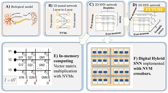
Figure 5.
NVM architectures. (A) Biological neuron. (B) Spiking neural network with spike-based learning implemented through NVMs. (C) Crossbar array for spiking neural network. Neuron and dynamic synapse circuits can be integrated into CMOS as in [160]. (D) Three-dimensional spiking neural network obtained stacking 2D synaptic arrays. (E) Multiplication matrix G is mapped onto NVM crossbar array. Input multiplication vector is defined in the analog domain by voltage vector. The output is the current vector, which represents the vector-matrix product. (F) SNN implemented with NVM crossbars that are connected through a time multiplexed interconnect network in a neuromorphic hardware architecture.
Although a lot of work has been carried out to integrate RRAM in 3D architectures, its challenge to avoid sneak path currents persists, which can be addressed by adding selector circuits with a highly nonlinear I-V capable of generating low leakage current [126]. In addition, researchers have been proposing devices Superlinear Threshold selector devices that include Mixed-Ionic-Electronic-Conduction (MIEC) based selector and Cu BEOL, compatible selector [161]. In Cu doped material, the tunneling layer helps in reducing the leakage current. The design has also shown high endurance capability. In [162], Esmanhotto et al. use multi-level programming on 3D integrated 1T-1R RRAM, exploring the opportunity of conductance relaxation to represent multiple bits. Commercial products of PCM have been proposed to facilitate large-scale integration [163]. Inherently, low power consuming STT-MRAM is an attractive choice for dense networks. In [164] by Yang et al., a pMTJ in 1S-1R configuration is proposed to achieve a 3D cross-point architecture of STT-MRAM architecture. The suggested selector with bidirectional threshold switching capability suppresses leakage current while providing sufficient ON current to turn on the synaptic elements.
Just like the work of [157], utilizing the benefit of hybrid architectures has made large-scale integration feasible. In [165] by Choi et al., a vertical organic synapse was proposed to feature a remote weight update implemented on a 3D crossbar array. However, many polymer OECT FETs have shown the behavior of a biological spiking synapse. In [166], Alibart et al. demonstrate the use of nanoparticle-organic hybrid device NOMFET to exhibit charge storage capability. In [167] by Kim et al., a semiconducting CNT channel along with an embedded floating gate is availed as a synaptic element. The channel conductance modulation in the floating gate is controlled with the additional CNT storage. Further, the design is more suitable to be integrated into flexible electronics because of CNT’s high flexibility. PCMs with their strong optical properties can be used as nonlinear photonic elements, but the speed of operation might have to increase to photonics modulation speeds [126].
5. SNN Edge Computing Architectures with NVMs
Emerging memory technologies and spiking neural networks are key enabling technologies in edge and extreme edge scenarios. These scenarios include tiny robotics, mobile devices, brain–machine interfaces, and biomedical signal processing with insertable and wearable devices that require ultra-low-power, high-density, and high throughput microchips. In this direction, the very recent work presented in [168] demonstrates a brain interface for spike sorting applications based on a high-density resistive crossbar that can perform in-memory spike sorting with ultra-low-power performances. The authors propose a template matching-based spike sorting algorithm that can be directly mapped onto an RRAM crossbar followed by a single layer of spiking neurons. This work shows the possibility of 3-D back-end-of-line (BEOL) integration with CMOS circuits to achieve extremely high throughput and efficient systems in scenarios that provide significant area, power, latency, and energy benefits.
In another recent work [160], a novel hardware calibrated learning rule for compensating heterogeneity in analog RRAM-based SSN crossbar has been presented. The authors demonstrate that by taking into account the measured heterogeneity characteristics during the off-chip learning phase, the hardware calibration SNN self-corrects its hardware nonidealities and solves benchmark temporal tasks such as ElectroCardioGram (ECG) audio classification with high accuracy and low energy.
In [169], Songdtco et al. propose a design technology co-optimization for RRAM-based neuromorphic computing for embedded and edge computing scenarios. Here, the authors show that the latency variation within crossbar hardware increases with technology scaling. This is due to the increase in the bitline and wordline parasitics. Latency variations lead to accuracy loss due to an increase in the inter-spike interval. However, technology scaling also offers benefits such as high integration density and lower power consumption. Authors show that by efficiently mapping neurons and synapses to the hardware while incorporating latency variations and by power-gating unused resources of a crossbar, the negative impacts of technology scaling could be mitigated. The authors show a significant increase in the classification accuracy using such neuron and synapse mapping strategies.
Similarly, in [82] Titirsha et al. propose a technique to improve the endurance of large PCM-based crossbar hardware. As the bit line and worldliness become longer, parasitic voltage drop increases the endurance. In the proposed technique, machine learning workloads map to memristors considering the endurance of the cell and the activation of neurons. In the work [170], the impact of resistance drifts during unsupervised learning on a PCM synapse. As discussed in Section 2, there has been a lot of research on mitigating the drift effect. However, these parameters were extracted from experiments and incorporated into the training model for solving the classification problem of handwritten digit recognition MNIST.
In another work [171] by Nomura et al., the authors conduct a simulation analysis to determine the effect of the number of conductance steps and process parameters on the PCM-based Restricted Boltzmann machine (RBM). Although PCM devices can achieve gradual SET operation, the RESET operation is difficult to control. Thus, the authors propose PCM-refresh, a method to update weight variation. Each synaptic weight is represented with two PCM devices corresponding to positive and negative conductance states. The resultant weight is the difference between both devices. It is observed that at least one-tenth of the conductance update must be accounted for to achieve comparable accuracy.
Apart from the most established PCM and RRAM architectures, in a recent work [172], Wang et al. implement two-layer fully connected spiking neural networks on binary MRAM synapses. Considering a sparse network, a simple peripheral interface is designed. Further, the weights are quantized to 8-bit width with a leaky integrate-and-fire neuron model. The design is learning compatible with low-cost hardware implementation. However, its performance metrics for MNIST dataset are not the best.
In [173], Jang et al. propose a stochastic multi-bit spin-orbit torque (SOT) MRAM-based crossbar array. The crossbar is further developed to form a complete Spiking neural network (SNN) hardware processor. One of the unique features of this implementation is the use of the Accumulative Spike technique. Compared to the conventional operation of accumulation of sparse presynaptic spikes at one instance, several presynaptic spikes from consecutive time steps are accumulated and processed in the crossbar array in the Accumulative Spike technique. Thus, improving the ADC utilization and reduced neuron updates. This architecture is compatible with both training and inference.
Further in Fang et al.’s work [174], a generalized Swarm Intelligence model on a spiking neural network is demonstrated in a 1T-1R FeFET-based neuron array. The network represents the agents in the swarm that is encoded as spiking inputs with a FeFET oscillator circuit. The oscillators are both inhibitory and excitatory. The inhibitory input is a winner-takes-all network that can mimic the path planning of ants more naturally. The neuron circuit design is compact and energy-efficient, showing promising potential for Swarm Intelligence on SNN.
6. Discussion and Conclusions
NVMs and SNNs can impact many application domains, given their assets and attributes (see Figure 6). The primitives’ attributes are compatible with biological computation. Still, they are not entirely found in modern hardware systems and with the same level of maturity as in the brain. NVMs and SNN can potentially bridge this gap by providing bio-inspired attributes to artificial intelligent systems.
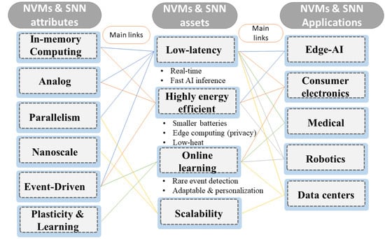
Figure 6.
Nonvolatile memories attributes, assets and application potentials.
Table 1 summarizes the read latency, write latency, and write endurance of different NVMs. PCM has come a long way, with enhancements in the high-volume memory domain, but there are delays in progress towards a higher endurance. One of the ways to address this is to engineer a PCM photonic device that employs its easy CMOS integration and builds on limited endurance PCM memristors. Although the inexpensive nature of PCM devices has brought them close to commercialization, their nonlinear accumulative behavior persists. CBRAM is the only emerging NVM that manifests the write speed as low as photonic devices of 1us with ultra-low power consumption. Suppose the cross-talk interference between adjacent memory cells in a crossbar is managed. In this case, CBRAM will be compatible with high-density silicon technologies.

Table 1.
Read latency, write latency, and write endurance of different NVMs.
Write speed close to what CBRAM can achieve is provided by FeFET devices with long endurance cycles. However, as discussed earlier, its destructive read cycle could potentially provide loss of information. Thus, ferroelectric-based circuits still have to be investigated. Spintronic-based MRAM technology has the ability to have almost infinite endurance at the proportional speed of an SRAM. The energy consumed per bit is much lower in MRAM NVM. A profuse amount of work has been conducted over the last decade on RRAM, but one of its drawbacks is its low reliability. This is evident from its finite data retention after repeated program/erase cycles. Although sneak path problems for RRAM crossbars have been extensively worked on, the need for architecture design enabling learning in biologically plausible function lasts. Nanowire-based 2 or 3 terminal RRAM could alleviate these issues with the addendum requirement of complex multiple interconnected network dynamics. Similarly, polymer technology has to be evolved in terms of its speed and density. But polymer merged PCM or RRAM devices have better scalability at a low cost. Currently, 2D materials seem attractive for in-sensor and in-memory computing with advancements in wafer-scale processing.
In general, NVMs can be used to enable massively parallel and distributed neuromorphic computing systems. However, there is still the need to design scalable, global learning architectures that can harness local spike-time-dependent plasticity rules for interesting computational tasks. Another critical aspect of neural-inspired computing systems is the sparsity of the activity, and NVMs architectures should harness such sparsity to reduce power consumption.
Today, compute-in-memory and near-memory computing that supports STDP learning still have to demonstrate competitive performance against state-of-the-art approaches in deep learning, and a better understanding of bio-inspired models of computation is still needed to unlock the potential of neuromorphic computing systems fully. Although some interesting preliminary demonstrations on image recognition [178] and biomedical temporal signal analysis [168] have been performed in NVMs spike-based neuromorphic systems. We are still missing fundamental understanding in creating a general architecture that can support learning. Such architecture should demonstrate accurate performance, exceeding traditional deep learning methods, but with a fraction of the energy, on nontrivial large-scale problems, such as natural language processing or vision-based benchmarks. Without such an understanding at both the algorithmic and architectural level, many neuromorphic systems are being benchmarked with the measure of power per spike (e.g., pJ per synaptic operation), even if it is unclear how many spikes are needed to perform a specific task. Additionally, it is unlikely that mean-rate models of spiking neural networks will bring substantial benefits in terms of energy, as they require a high number of spikes to achieve high-numerical value precision. Nevertheless, spike sparsity and a single spike encoding strategies, such as inter-spike-interval coding [179], time-to-first-spike [180], or time-delay coding [181], hold great potential in reducing the communication and the energy of neural-inspired information processing systems. Today, the state-of-the-art SNN models demonstrate competitive performance on small-scale benchmarks with recurrent spiking neural networks and spiking convolutional models, approaching or exceeding traditional deep learning networks with a similar number of parameters but with a fraction of required operations [8]. These recent achievements open opportunities for designing novel architectures that can best exploit sparsity as one of the crucial ingredients necessary in achieving low-power performances.
On the other hand, traditional deep learning neural networks with supervised, self-supervised error backpropagation are already being applied in real-world applications in the context of speech recognition, recommendation systems, self-driving cars, autonomous drones, and other emerging applications. These algorithms require the execution of large multiply-accumulate operations in the form of vector-matrix multiplication, and because of the limitation of traditional compute architectures, their power performance doesn’t scale well with the complexity of the models. Fortunately, NVMs can potentially impact traditional deep learning accelerators by providing in-memory computing abilities. In fact, their conductance pairs can be used to represent the weight values, and multiply-accumulate operations can be carried out in the analog domain. Analog implementation of matrix-vector-multiplications is an interesting direction currently being explored with traditional CMOS processes for enabling power-efficient deep learning accelerators [182,183]. These accelerators can also potentially benefit from NVMs as well. However, there is still the need to demonstrate these advantages in actual hardware systems at the scale at which they are useful, demonstrating clear advantages over traditional deep learning models. Additionally, integrating NVMs in traditional hardware will require the creation of novel self-calibrating and self-learning mechanisms capable of compensating for internal and external disturbances, such as drifts over time, endurance problems, noise, and variability.
Currenly, much research is devoted to fabricating ideal NVMs. In contrast to conventional data storage systems, device history is a fundamental property exploited for learning and programmability. And even if neuromorphic systems have shown to support and embrace device variability and nonidealities, they still fail to fully benefit from asymmetry and nonlinearities of conductance responses. For these reasons, an ideal NVM device should provide an almost linear response over most of its conductance, and each programming pulse should only marginally change its conductance response of only a small portion of the linear regime. Still, we miss a basic algorithmic understanding of exploiting variability and inhomogeneity in the computing substrate. Such properties seem to be present in any neural system suggesting that nature has solved these problems. Nevertheless, today, much research is devoted to trying to solve the issues of of linearity and programmability without suffering from some kind of side effect, while little is being done to try to cope with these nonidealities at the algorithmic level. For example, CBRAM devices offer a large dynamic range. However, the filament process is abrupt and discontinuous. The filament RRAM also suffers from a lower dynamic range and abrupt programming. As binary devices or stochastic elements can indeed be integrated with neuromorphic systems, it is still unclear what models of computation compensate for these stochasticities. Concerning the symmetry of responses, RRAM offers bidirectional changes. Still, these are often nonlinear and hardly scale to low voltages for extreme low-power operations.
Finally, the implementation of the physical properties of synapses and neurons with NVM devices seems to be beneficial not only for neuromorphic devices but also for in-memory and near-memory applications. In such scenarios, what is really required from the research community is a compelling demonstration that can showcase the energy, speed, cost, density, or other advantages for such systems that justify the costly process of developing new semiconductor processes at a scale compatible with CMOS technology.
Even if many problems related to the device, circuit, system, architecture, and computational modeling remain to be solved with new knowledge, the application and research of NVMs for neuromorphic computing devices continue to produce attractive solutions for bio-inspired models of computations. These models require massive parallelism, in-memory, close to memory computing abilities, and distributed information processing strategies such as online learning and adaptation while processing enormous data. NVM devices are expected to contribute to the emerging field of modern computing and will remain an active research direction for decades.
Author Contributions
Writing—review and editing, M.L.V., F.C. and A.D. All authors have read and agreed to the published version of the manuscript.
Funding
This material is based upon work supported by the U.S. Department of Energy under Award Number DE-SC0022014 and by the National Science Foundation under Grant Nos. CCF-1942697 and CCF-1937419.
Conflicts of Interest
The authors declare no conflict of interest.
References
- Mead, C. Neuromorphic electronic systems. Proc. IEEE 1990, 78, 1629–1636. [Google Scholar] [CrossRef] [Green Version]
- Maass, W. Networks of spiking neurons: The third generation of neural network models. Neural Netw. 1997, 10, 1659–1671. [Google Scholar] [CrossRef]
- Sengupta, A.; Ye, Y.; Wang, R.; Liu, C.; Roy, K. Going deeper in spiking neural networks: VGG and residual architectures. Front. Neurosci. 2019, 13, 95. [Google Scholar] [CrossRef] [PubMed]
- Das, A.; Pradhapan, P.; Groenendaal, W.; Adiraju, P.; Rajan, R.; Catthoor, F.; Schaafsma, S.; Krichmar, J.; Dutt, N.; Van Hoof, C. Unsupervised heart-rate estimation in wearables with Liquid states and a probabilistic readout. Neural Netw. 2018, 99, 134–147. [Google Scholar] [CrossRef] [Green Version]
- Balaji, A.; Corradi, F.; Das, A.; Pande, S.; Schaafsma, S.; Catthoor, F. Power-accuracy trade-offs for heartbeat classification on neural networks hardware. J. Low Power Electron. 2018, 14, 508–519. [Google Scholar] [CrossRef] [Green Version]
- Hu, Y.; Tang, H.; Pan, G. Spiking Deep Residual Networks. IEEE Trans. Neural Netw. Learn. Syst. 2018, 1–6. Available online: https://ieeexplore.ieee.org/abstract/document/9597475 (accessed on 16 March 2022). [CrossRef]
- Bohte, S.M.; Kok, J.N.; La Poutré, J.A. SpikeProp: Backpropagation for networks of spiking neurons. In Proceedings of the European Symposium on Artificial Neural Networks, Bruges, Belgium, 26–28 April 2000. [Google Scholar]
- Yin, B.; Corradi, F.; Bohté, S.M. Accurate and efficient time-domain classification with adaptive spiking recurrent neural networks. Nat. Mach. Intell. 2021, 3, 905–913. [Google Scholar] [CrossRef]
- Perez-Nieves, N.; Goodman, D. Sparse spiking gradient descent. NeurIPS 2021, 34. Available online: https://proceedings.neurips.cc/paper/2021/hash/61f2585b0ebcf1f532c4d1ec9a7d51aa-Abstract.html (accessed on 16 March 2022).
- Davies, M. Benchmarks for progress in neuromorphic computing. Nat. Mach. Intell. 2019, 1, 386–388. [Google Scholar] [CrossRef]
- Das, A.; Catthoor, F.; Schaafsma, S. Heartbeat classification in wearables using multi-layer perceptron and time-frequency joint distribution of ECG. In Proceedings of the 2018 IEEE/ACM International Conference on Connected Health: Applications, Systems and Engineering Technologies, Washington, DC, USA, 26–28 September 2018. [Google Scholar]
- Corradi, F.; Pande, S.; Stuijt, J.; Qiao, N.; Schaafsma, S.; Indiveri, G.; Catthoor, F. ECG-based heartbeat classification in neuromorphic hardware. In Proceedings of the 2019 International Joint Conference on Neural Networks (IJCNN), Budapest, Hungary, 14–19 July 2019. [Google Scholar]
- Furber, S. Large-scale neuromorphic computing systems. J. Neural Eng. 2016, 13, 051001. [Google Scholar] [CrossRef]
- Schuman, C.D.; Potok, T.E.; Patton, R.M.; Birdwell, J.D.; Dean, M.E.; Rose, G.S.; Plank, J.S. A survey of neuromorphic computing and neural networks in hardware. arXiv 2017, arXiv:1705.06963. [Google Scholar]
- Marković, D.; Mizrahi, A.; Querlioz, D.; Grollier, J. Physics for neuromorphic computing. Nat. Rev. Phys. 2020, 2, 499–510. [Google Scholar] [CrossRef]
- Burr, G.W.; Shelby, R.M.; Sebastian, A.; Kim, S.; Kim, S.; Sidler, S.; Virwani, K.; Ishii, M.; Narayanan, P.; Fumarola, A.; et al. Neuromorphic computing using non-volatile memory. Adv. Phys. X 2017, 2, 89–124. [Google Scholar] [CrossRef]
- Esser, S.K.; Appuswamy, R.; Merolla, P.; Arthur, J.V.; Modha, D.S. Backpropagation for energy-efficient neuromorphic computing. NeurIPS 2015, 28. Available online: https://proceedings.neurips.cc/paper/2015/hash/10a5ab2db37feedfdeaab192ead4ac0e-Abstract.html (accessed on 16 March 2022).
- Indiveri, G.; Liu, S.C. Memory and information processing in neuromorphic systems. Proc. IEEE 2015, 103, 1379–1397. [Google Scholar] [CrossRef] [Green Version]
- Lin, C.K.; Wild, A.; Chinya, G.N.; Lin, T.H.; Davies, M.; Wang, H. Mapping Spiking Neural Networks onto a Manycore Neuromorphic Architecture. ACM SIGPLAN Notice 2018, 53, 78–89. [Google Scholar] [CrossRef]
- Das, A.; Wu, Y.; Huynh, K.; Dell’Anna, F.; Catthoor, F.; Schaafsma, S. Mapping of local and global synapses on spiking neuromorphic hardware. In Proceedings of the 2018 Design, Automation & Test in Europe Conference & Exhibition (DATE), Dresden, Germany, 19–23 March 2018. [Google Scholar]
- Ji, Y.; Zhang, Y.; Li, S.; Chi, P.; Jiang, C.; Qu, P.; Xie, Y.; Chen, W. NEUTRAMS: Neural network transformation and co-design under neuromorphic hardware constraints. In Proceedings of the 2016 49th Annual IEEE/ACM International Symposium on Microarchitecture (MICRO), Taipei, Taiwan, 15–19 October 2016. [Google Scholar]
- Balaji, A.; Das, A.; Wu, Y.; Huynh, K.; Dell’anna, F.G.; Indiveri, G.; Krichmar, J.L.; Dutt, N.D.; Schaafsma, S.; Catthoor, F. Mapping spiking neural networks to neuromorphic hardware. IEEE Trans. Very Large Scale Integr. Syst. 2020, 28, 76–86. [Google Scholar] [CrossRef]
- Song, S.; Chong, H.; Balaji, A.; Das, A.; Shackleford, J.; Kandasamy, N. DFSynthesizer: Dataflow-based synthesis of spiking neural networks to neuromorphic hardware. ACM Trans. Embed. Comput. Syst. 2021. [Google Scholar] [CrossRef]
- Titirsha, T.; Song, S.; Balaji, A.; Das, A. On the Role of System Software in Energy Management of Neuromorphic Computing. In Proceedings of the 18th ACM International Conference on Computing Frontiers, Virtual, 11–13 May 2021; pp. 124–132. [Google Scholar] [CrossRef]
- Paul, A.; Tajin, M.A.S.; Das, A.; Mongan, W.; Dandekar, K. Energy-Efficient Respiratory Anomaly Detection in Premature Newborn Infants. Electronics 2022, 11, 682. [Google Scholar] [CrossRef]
- Balaji, A.; Adiraju, P.; Kashyap, H.J.; Das, A.; Krichmar, J.L.; Dutt, N.D.; Catthoor, F. PyCARL: A PyNN interface for hardware-software co-simulation of spiking neural network. arXiv 2020, arXiv:2003.09696. [Google Scholar]
- Curzel, S.; Agostini, N.B.; Song, S.; Dagli, I.; Limaye, A.; Tan, C.; Minutoli, M.; Castellana, V.G.; Amatya, V.; Manzano, J.; et al. Automated Generation of Integrated Digital and Spiking Neuromorphic Machine Learning Accelerators. In Proceedings of the 2021 IEEE/ACM International Conference On Computer Aided Design (ICCAD), Munich, Germany, 1–4 November 2021. [Google Scholar]
- Song, S.; Mirtinti, L.V.; Das, A.; Kandasamy, N. A Design Flow for Mapping Spiking Neural Networks to Many-Core Neuromorphic Hardware. In Proceedings of the 2021 IEEE/ACM International Conference On Computer Aided Design (ICCAD), Munich, Germany, 1–4 November 2021. [Google Scholar]
- Huynh, P.K.; Varshika, M.L.; Paul, A.; Isik, M.; Balaji, A.; Das, A. Implementing Spiking Neural Networks on Neuromorphic Architectures: A Review. arXiv 2022, arXiv:2202.08897. [Google Scholar]
- Varshika, M.L.; Balaji, A.; Corradi, F.; Das, A.; Stuijt, J.; Catthoor, F. Design of Many-Core Big Little μBrains for Energy-Efficient Embedded Neuromorphic Computing. arXiv 2021, arXiv:arXiv:2111.11838. [Google Scholar]
- Balaji, A.; Song, S.; Titirsha, T.; Das, A.; Krichmar, J.; Dutt, N.; Shackleford, J.; Kandasamy, N.; Catthoor, F. NeuroXplorer 1.0: An Extensible Framework for Architectural Exploration with Spiking Neural Networks. In Proceedings of the International Conference on Neuromorphic Systems 2021, Knoxville, TN, USA, 27–29 July 2021. [Google Scholar]
- Furber, S.; Galluppi, F.; Temple, S.; Plana, L.A. The SpiNNaker project. Proc. IEEE 2014, 102, 652–665. [Google Scholar] [CrossRef]
- Debole, M.V.; Taba, B.; Amir, A.; Akopyan, F.; Andreopoulos, A.; Risk, W.P.; Kusnitz, J.; Otero, C.O.; Nayak, T.K.; Appuswamy, R.; et al. TrueNorth: Accelerating from zero to 64 million neurons in 10 years. Computer 2019, 52, 20–29. [Google Scholar] [CrossRef]
- Davies, M.; Srinivasa, N.; Lin, T.H.; Chinya, G.; Cao, Y.; Choday, S.H.; Dimou, G.; Joshi, P.; Imam, N.; Jain, S.; et al. Loihi: A neuromorphic manycore processor with on-chip learning. IEEE Micro 2018, 38, 82–99. [Google Scholar] [CrossRef]
- Stuijt, J.; Sifalakis, M.; Yousefzadeh, A.; Corradi, F. μBrain: An Event-Driven and Fully Synthesizable Architecture for Spiking Neural Networks. Front. Neurosci. 2021, 15, 538. [Google Scholar] [CrossRef]
- Frenkel, C.; Lefebvre, M.; Legat, J.D.; Bol, D. A 0.086-mm2 12.7-pJ/SOP 64k-synapse 256-neuron online-learning digital spiking neuromorphic processor in 28-nm CMOS. IEEE Trans. Biomed. Circuits Syst. 2019, 13, 145–158. [Google Scholar]
- Benjamin, B.; Gao, P.; McQuinn, E.; Choudhary, S.; Chandrasekaran, A.R.; Bussat, J.M.; Alvarez-Icaza, R.; Arthur, J.V.; Merolla, P.A.; Boahen, K. Neurogrid: A mixed-analog-digital multichip system for large-scale neural simulations. Proc. IEEE 2014, 102, 699–716. [Google Scholar] [CrossRef]
- Schemmel, J.; Grübl, A.; Hartmann, S.; Kononov, A.; Mayr, C.; Meier, K.; Millner, S.; Partzsch, J.; Schiefer, S.; Scholze, S.; et al. Live demonstration: A scaled-down version of the brainscales wafer-scale neuromorphic system. In Proceedings of the 2012 IEEE international symposium on circuits and systems (ISCAS), Seoul, Korea, 20–23 May 2012. [Google Scholar]
- Shi, L.; Pei, J.; Deng, N.; Wang, D.; Deng, L.; Wang, Y.; Zhang, Y.; Chen, F.; Zhao, M.; Song, S.; et al. Development of a neuromorphic computing system. In Proceedings of the 2015 IEEE International Electron Devices Meeting (IEDM), Washington, DC, USA, 7–9 December 2015. [Google Scholar]
- Chi, P.; Li, S.; Xu, C.; Zhang, T.; Zhao, J.; Liu, Y.; Wang, Y.; Xie, Y. PRIME: A Novel Processing-in-Memory Architecture for Neural Network Computation in ReRAM-Based Main Memory. ACM Sigarch Comput. Archit. News 2016, 44, 27–39. [Google Scholar] [CrossRef]
- Moradi, S.; Qiao, N.; Stefanini, F.; Indiveri, G. A scalable multicore architecture with heterogeneous memory structures for dynamic neuromorphic asynchronous processors (DYNAPs). IEEE Trans. Biomed. Circuits Syst. 2017, 12, 106–122. [Google Scholar] [CrossRef] [Green Version]
- Xia, Q.; Yang, J.J. Memristive crossbar arrays for brain-inspired computing. Nat. Mater. 2019, 18, 309–323. [Google Scholar] [CrossRef] [PubMed]
- Chakraborty, I.; Jaiswal, A.; Saha, A.; Gupta, S.; Roy, K. Pathways to efficient neuromorphic computing with non-volatile memory technologies. Appl. Phys. Rev. 2020, 7, 021308. [Google Scholar] [CrossRef]
- Islam, R.; Li, H.; Chen, P.Y.; Wan, W.; Chen, H.Y.; Gao, B.; Wu, H.; Yu, S.; Saraswat, K.; Wong, H.P. Device and materials requirements for neuromorphic computing. J. Phys. Appl. Phys. 2019, 52, 113001. [Google Scholar] [CrossRef]
- Chen, A. A review of emerging non-volatile memory (NVM) technologies and applications. Solid-State Electron. 2016, 125, 25–38. [Google Scholar] [CrossRef]
- Liu, D.; Yu, H.; Chai, Y. Low-power computing with neuromorphic engineering. Adv. Intell. Syst. 2021, 3, 2000150. [Google Scholar] [CrossRef]
- Strenz, R. Review and outlook on embedded nvm technologies–from evolution to revolution. In Proceedings of the 2020 IEEE International Memory Workshop (IMW), Dresden, Germany, 17–20 May 2020. [Google Scholar]
- Burr, G.W.; Sebastian, A.; Vianello, E.; Waser, R.; Parkin, S. Emerging materials in neuromorphic computing: Guest editorial. APL Mater. 2020, 8, 010401. [Google Scholar] [CrossRef]
- Mehonic, A.; Sebastian, A.; Rajendran, B.; Simeone, O.; Vasilaki, E.; Kenyon, A.J. Memristors—From In-Memory Computing, Deep Learning Acceleration, and Spiking Neural Networks to the Future of Neuromorphic and Bio-Inspired Computing. Adv. Intell. Syst. 2020, 2, 2000085. [Google Scholar] [CrossRef]
- Lee, B.; Ipek, E.; Mutlu, O.; Burger, D. Architecting Phase Change Memory As a Scalable DRAM Alternative. In Proceedings of the 36th annual international symposium on Computer architecture, Austin, TX, USA, 20–24 June 2009. [Google Scholar]
- Mutlu, O. Memory scaling: A systems architecture perspective. In Proceedings of the 2013 5th IEEE International Memory Workshop, Monterey, CA, USA, 26–29 May 2013. [Google Scholar]
- Song, S.; Das, A.; Kandasamy, N. Exploiting Inter- and Intra-Memory Asymmetries for Data Mapping in Hybrid Tiered-Memories. In Proceedings of the 2020 ACM SIGPLAN International Symposium on Memory Management, London, UK, 16 June 2020. [Google Scholar]
- Eisenman, A.; Gardner, D.; AbdelRahman, I.; Axboe, J.; Dong, S.; Hazelwood, K.; Petersen, C.; Cidon, A.; Katti, S. Reducing DRAM footprint with NVM in Facebook. In Proceedings of the Thirteenth EuroSys Conference, Porto, Portugal, 23–26 April 2018. [Google Scholar]
- Burr, G.W.; Kurdi, B.N.; Scott, J.C.; Lam, C.H.; Gopalakrishnan, K.; Shenoy, R.S. Overview of candidate device technologies for storage-class memory. IBM J. Res. Dev. 2008, 52, 449–464. [Google Scholar] [CrossRef] [Green Version]
- Kuzum, D.; Yu, S.; Wong, H.P. Synaptic electronics: Materials, devices and applications. Nanotechnology 2013, 24, 382001. [Google Scholar] [CrossRef]
- Giulioni, M.; Corradi, F.; Dante, V.; Del Giudice, P. Real time unsupervised learning of visual stimuli in neuromorphic VLSI systems. Sci. Rep. 2015, 5, 14730. [Google Scholar] [CrossRef] [Green Version]
- Burr, G.W.; Shelby, R.M.; Sidler, S.; Di Nolfo, C.; Jang, J.; Boybat, I.; Shenoy, R.S.; Narayanan, P.; Virwani, K.; Giacometti, E.U.; et al. Experimental demonstration and tolerancing of a large-scale neural network (165,000 synapses) using phase-change memory as the synaptic weight element. IEEE Trans. Electron Devices 2015, 62, 3498–3507. [Google Scholar] [CrossRef]
- Yan, Y.; Wu, X.; Chen, Q.; Wang, X.; Li, E.; Liu, Y.; Chen, H.; Guo, T. An intrinsically healing artificial neuromorphic device. J. Mater. Chem. C 2020, 8, 6869–6876. [Google Scholar] [CrossRef]
- Song, Z.; Wang, R.; Xue, Y.; Song, S. The “gene” of reversible phase transformation of phase change materials: Octahedral motif. Nano Res. 2022, 15, 765–772. [Google Scholar] [CrossRef]
- Lee, H.; Chen, P.; Wu, T.; Chen, Y.; Wang, C.; Tzeng, P.; Lin, C.; Chen, F.; Lien, C.; Tsai, M.J. Low power and high speed bipolar switching with a thin reactive Ti buffer layer in robust HfO2 based RRAM. In Proceedings of the 2008 IEEE International Electron Devices Meeting, San Francisco, CA, USA, 15–17 December 2008. [Google Scholar]
- Wu, L.; Taouil, M.; Rao, S.; Marinissen, E.J.; Hamdioui, S. Electrical modeling of STT-MRAM defects. In Proceedings of the 2018 IEEE International Test Conference (ITC), Phoenix, AZ, USA, 29 October–1 November 2018. [Google Scholar]
- Luo, Z.D.; Zhang, S.; Liu, Y.; Zhang, D.; Gan, X.; Seidel, J.; Liu, Y.; Han, G.; Alexe, M.; Hao, Y. Dual-Ferroelectric-Coupling-Engineered Two-Dimensional Transistors for Multifunctional In-Memory Computing. ACS Nano 2022, 16, 3362–3372. [Google Scholar] [CrossRef]
- Di Bartolomeo, A.; Rinzan, M.; Boyd, A.K.; Yang, Y.; Guadagno, L.; Giubileo, F.; Barbara, P. Electrical properties and memory effects of field-effect transistors from networks of single-and double-walled carbon nanotubes. Nanotechnology 2010, 21, 115204. [Google Scholar] [CrossRef]
- Lu, W.; Xie, P.; Lieber, C.M. Nanowire transistor performance limits and applications. IEEE Trans. Electron Devices 2008, 55, 2859–2876. [Google Scholar] [CrossRef]
- Yang, J.M.; Choi, E.S.; Kim, S.Y.; Kim, J.H.; Park, J.H.; Park, N.G. Perovskite-related (CH 3 NH 3) 3 Sb 2 Br 9 for forming-free memristor and low-energy-consuming neuromorphic computing. Nanoscale 2019, 11, 6453–6461. [Google Scholar] [CrossRef]
- Farmer, D.B.; Chiu, H.Y.; Lin, Y.M.; Jenkins, K.A.; Xia, F.; Avouris, P. Utilization of a buffered dielectric to achieve high field-effect carrier mobility in graphene transistors. Nano Lett. 2009, 9, 4474–4478. [Google Scholar] [CrossRef] [Green Version]
- Goswami, S.; Matula, A.J.; Rath, S.P.; Hedström, S.; Saha, S.; Annamalai, M.; Sengupta, D.; Patra, A.; Ghosh, S.; Jani, H.; et al. Robust resistive memory devices using solution-processable metal-coordinated azo aromatics. Nat. Mater. 2017, 16, 1216–1224. [Google Scholar] [CrossRef]
- Wong, H.S.P.; Raoux, S.; Kim, S.; Liang, J.; Reifenberg, J.P.; Rajendran, B.; Asheghi, M.; Goodson, K.E. Phase change memory. Proc. IEEE 2010, 98, 2201–2227. [Google Scholar] [CrossRef]
- Burr, G.W.; Breitwisch, M.J.; Franceschini, M.; Garetto, D.; Gopalakrishnan, K.; Jackson, B.; Kurdi, B.; Lam, C.; Lastras, L.A.; Padilla, A.; et al. Phase change memory technology. J. Vac. Sci. Technol. Nanotechnol. Microelectron. Mater. Process. Meas. Phenom. 2010, 28, 223–262. [Google Scholar] [CrossRef] [Green Version]
- Bez, R. Chalcogenide PCM: A memory technology for next decade. In Proceedings of the 2009 IEEE International Electron Devices Meeting (IEDM), Baltimore, MD, USA, 7–9 December 2009. [Google Scholar]
- Jones, R.O. Phase change memory materials: Rationalizing the dominance of Ge/Sb/Te alloys. Phys. Rev. B 2020, 101, 024103. [Google Scholar] [CrossRef]
- Raoux, S.; Xiong, F.; Wuttig, M.; Pop, E. Phase change materials and phase change memory. MRS Bull. 2014, 39, 703–710. [Google Scholar] [CrossRef] [Green Version]
- Zahoor, F.; Azni Zulkifli, T.Z.; Khanday, F.A. Resistive random access memory (RRAM): An overview of materials, switching mechanism, performance, multilevel cell (MLC) storage, modeling, and applications. Nanoscale Res. Lett. 2020, emph15, 1–26. [Google Scholar] [CrossRef] [PubMed]
- Papandreou, N.; Pantazi, A.; Sebastian, A.; Breitwisch, M.; Lam, C.; Pozidis, H.; Eleftheriou, E. Multilevel phase-change memory. In Proceedings of the 2010 17th IEEE International Conference on Electronics, Circuits and Systems, Athens, Greece, 12–15 December 2010. [Google Scholar]
- Stanisavljevic, M.; Pozidis, H.; Athmanathan, A.; Papandreou, N.; Mittelholzer, T.; Eleftheriou, E. Demonstration of reliable triple-level-cell (TLC) phase-change memory. In Proceedings of the 2016 IEEE 8th International Memory Workshop (IMW), Paris, France, 15–18 May 2016. [Google Scholar]
- Sebastian, A.; Le Gallo, M.; Burr, G.W.; Kim, S.; BrightSky, M.; Eleftheriou, E. Tutorial: Brain-inspired computing using phase-change memory devices. J. Appl. Phys. 2018, 124, 111101. [Google Scholar] [CrossRef] [Green Version]
- Kuzum, D.; Jeyasingh, R.G.; Lee, B.; Wong, H.S.P. Nanoelectronic programmable synapses based on phase change materials for brain-inspired computing. Nano Lett. 2012, 12, 2179–2186. [Google Scholar] [CrossRef] [PubMed]
- Caporale, N.; Dan, Y. Spike timing–dependent plasticity: A Hebbian learning rule. Annu. Rev. Neurosci. 2008, 31, 25–46. [Google Scholar] [CrossRef] [Green Version]
- Bichler, O.; Suri, M.; Querlioz, D.; Vuillaume, D.; DeSalvo, B.; Gamrat, C. Visual pattern extraction using energy-efficient 2-PCM synapse neuromorphic architecture. IEEE Trans. Electron Devices 2012, 59, 2206–2214. [Google Scholar] [CrossRef]
- Kuzum, D.; Jeyasingh, R.G.; Wong, H.S.P. Energy efficient programming of nanoelectronic synaptic devices for large-scale implementation of associative and temporal sequence learning. In Proceedings of the 2011 International Electron Devices Meeting, Washington, DC, USA, 5–7 December 2011. [Google Scholar]
- Li, Y.; Zhong, Y.; Xu, L.; Zhang, J.; Xu, X.; Sun, H.; Miao, X. Ultrafast synaptic events in a chalcogenide memristor. Sci. Rep. 2013, 3, 1619. [Google Scholar] [CrossRef] [Green Version]
- Titirsha, T.; Song, S.; Das, A.; Krichmar, J.; Dutt, N.; Kandasamy, N.; Catthoor, F. Endurance-Aware Mapping of Spiking Neural Networks to Neuromorphic Hardware. IEEE Trans. Parallele Distrib. Syst. 2021, 33, 288–301. [Google Scholar] [CrossRef]
- Titirsha, T.; Das, A. Thermal-Aware Compilation of Spiking Neural Networks to Neuromorphic Hardware. arXiv 2020, arXiv:2010.04773. [Google Scholar]
- Eryilmaz, S.B.; Kuzum, D.; Jeyasingh, R.G.; Kim, S.; BrightSky, M.; Lam, C.; Wong, H.S.P. Experimental demonstration of array-level learning with phase change synaptic devices. In Proceedings of the 2013 IEEE International Electron Devices Meeting, Washington, DC, USA, 9–11 December 2013. [Google Scholar]
- Ambrogio, S.; Narayanan, P.; Tsai, H.; Shelby, R.M.; Boybat, I.; Di Nolfo, C.; Sidler, S.; Giordano, M.; Bodini, M.; Farinha, N.C.; et al. Equivalent-accuracy accelerated neural-network training using analogue memory. Nature 2018, 558, 60–67. [Google Scholar] [CrossRef] [PubMed]
- Song, S.; Das, A. A case for lifetime reliability-aware neuromorphic computing. arXiv 2020, arXiv:2007.02210. [Google Scholar]
- Kundu, S.; Basu, K.; Sadi, M.; Titirsha, T.; Song, S.; Das, A.; Guin, U. Special Session: Reliability Analysis for ML/AI Hardware. arXiv 2021, arXiv:2103.12166. [Google Scholar]
- Balaji, A.; Song, S.; Das, A.; Dutt, N.; Krichmar, J.; Kandasamy, N.; Catthoor, F. A framework to explore workload-specific performance and lifetime trade-offs in neuromorphic computing. IEEE Comput. Archit. Lett. 2019, 18, 149–152. [Google Scholar] [CrossRef] [Green Version]
- Song, S.; Das, A.; Kandasamy, N. Improving dependability of neuromorphic computing with non-volatile memory. arXiv 2020, arXiv:2006.05868. [Google Scholar]
- Song, S.; Hanamshet, J.; Balaji, A.; Das, A.; Krichmar, J.; Dutt, N.; Kandasamy, N.; Catthoor, F. Dynamic reliability management in neuromorphic computing. ACM J. Emerg. Technol. Comput. Syst. 2021, 17, 1–27. [Google Scholar] [CrossRef]
- Kim, I.; Cho, S.; Im, D.; Cho, E.; Kim, D.; Oh, G.; Ahn, D.; Park, S.; Nam, S.; Moon, J.; et al. High performance PRAM cell scalable to sub-20nm technology with below 4F2 cell size, extendable to DRAM applications. In Proceedings of the 2010 Symposium on VLSI Technology, Honolulu, HI, USA, 15–17 June 2010. [Google Scholar]
- Wang, L.; Yang, C.H.; Wen, J. Physical principles and current status of emerging non-volatile solid state memories. Electron. Mater. Lett. 2015, 11, 505–543. [Google Scholar] [CrossRef]
- Burr, G.; Virwani, K.; Shenoy, R.; Fraczak, G.; Rettner, C.; Padilla, A.; King, R.; Nguyen, K.; Bowers, A.; Jurich, M.; et al. Recovery dynamics and fast (sub-50ns) read operation with access devices for 3D crosspoint memory based on mixed-ionic-electronic-conduction (MIEC). In Proceedings of the 2013 Symposium on VLSI Technology, Kyoto, Japan, 11–13 June 2013. [Google Scholar]
- Pirovano, A.; Lacaita, A.L.; Pellizzer, F.; Kostylev, S.A.; Benvenuti, A.; Bez, R. Low-field amorphous state resistance and threshold voltage drift in chalcogenide materials. IEEE Trans. Electron Devices 2004, 51, 714–719. [Google Scholar] [CrossRef]
- Dirisaglik, F.; Bakan, G.; Jurado, Z.; Muneer, S.; Akbulut, M.; Rarey, J.; Sullivan, L.; Wennberg, M.; King, A.; Zhang, L.; et al. High speed, high temperature electrical characterization of phase change materials: Metastable phases, crystallization dynamics, and resistance drift. Nanoscale 2015, 7, 16625–16630. [Google Scholar] [CrossRef]
- Titirsha, T.; Das, A. Reliability-Performance Trade-offs in Neuromorphic Computing. In Proceedings of the 2020 11th International Green and Sustainable Computing Workshops (IGSC), Pullman, WA, USA, 19–22 October 2020. [Google Scholar]
- Hickmott, T. Low-frequency negative resistance in thin anodic oxide films. J. Appl. Phys. 1962, 33, 2669–2682. [Google Scholar] [CrossRef]
- Akinaga, H.; Shima, H. Resistive random access memory (ReRAM) based on metal oxides. Proc. IEEE 2010, 98, 2237–2251. [Google Scholar] [CrossRef]
- Burkitt, A.N. A review of the integrate-and-fire neuron model: I. Homogeneous synaptic input. Biol. Cybern. 2006, 95, 1–19. [Google Scholar] [CrossRef]
- Prezioso, M.; Merrikh Bayat, F.; Hoskins, B.; Likharev, K.; Strukov, D. Self-adaptive spike-time-dependent plasticity of metal-oxide memristors. Sci. Rep. 2016, 6, 21331. [Google Scholar] [CrossRef] [PubMed]
- Yu, S.; Wu, Y.; Jeyasingh, R.; Kuzum, D.; Wong, H.S.P. An electronic synapse device based on metal oxide resistive switching memory for neuromorphic computation. IEEE Trans. Electron Devices 2011, 58, 2729–2737. [Google Scholar] [CrossRef]
- Valentian, A.; Rummens, F.; Vianello, E.; Mesquida, T.; de Boissac, C.L.M.; Bichler, O.; Reita, C. Fully integrated spiking neural network with analog neurons and RRAM synapses. In Proceedings of the 2019 IEEE International Electron Devices Meeting (IEDM), San Francisco, CA, USA, 7–11 December 2019. [Google Scholar]
- Hansen, M.; Ziegler, M.; Kolberg, L.; Soni, R.; Dirkmann, S.; Mussenbrock, T.; Kohlstedt, H. A double barrier memristive device. Sci. Rep. 2015, 5, 13753. [Google Scholar] [CrossRef] [Green Version]
- Yang, R.; Terabe, K.; Yao, Y.; Tsuruoka, T.; Hasegawa, T.; Gimzewski, J.K.; Aono, M. Synaptic plasticity and memory functions achieved in a WO3-x-based nanoionics device by using the principle of atomic switch operation. Nanotechnology 2013, 24, 384003. [Google Scholar] [CrossRef]
- Goux, L.; Valov, I. Electrochemical processes and device improvement in conductive bridge RAM cells. Phys. Status Solidi 2016, 213, 274–288. [Google Scholar] [CrossRef]
- Fackenthal, R.; Kitagawa, M.; Otsuka, W.; Prall, K.; Mills, D.; Tsutsui, K.; Javanifard, J.; Tedrow, K.; Tsushima, T.; Shibahara, Y.; et al. 19.7 A 16 Gb ReRAM with 200 MB/s write and 1 GB/s read in 27 nm technology. In Proceedings of the 2014 IEEE International Solid-State Circuits Conference Digest of Technical Papers (ISSCC), San Francisco, CA, USA, 9–13 February 2014. [Google Scholar]
- Wijesinghe, P.; Ankit, A.; Sengupta, A.; Roy, K. An all-memristor deep spiking neural computing system: A step toward realizing the low-power stochastic brain. IEEE Trans. Emerg. Top. Comput. Intell. 2018, 2, 345–358. [Google Scholar] [CrossRef]
- Shim, W.; Luo, Y.; Seo, J.s.; Yu, S. Impact of read disturb on multilevel RRAM based inference engine: Experiments and model prediction. In Proceedings of the 2020 IEEE International Reliability Physics Symposium (IRPS), Dallas, TX, USA, 28 April–30 May 2020. [Google Scholar]
- Song, S.; Titirsha, T.; Das, A. Improving Inference Lifetime of Neuromorphic Systems via Intelligent Synapse Mapping. In Proceedings of the 2021 IEEE 32nd International Conference on Application-Specific Systems, Architectures and Processors (ASAP), Virtual, 7–9 July 2021. [Google Scholar]
- Paul, A.; Das, A. Design Technology Co-Optimization for Neuromorphic Computing. In Proceedings of the 2021 12th International Green and Sustainable Computing Conference (IGSC), Pullman, WA, USA, 18–21 October 2021. [Google Scholar]
- Paul, A.; Song, S.; Titirsha, T.; Das, A. On the Mitigation of Read Disturbances in Neuromorphic Inference Hardware. arXiv 2022, arXiv:2201.11527. [Google Scholar] [CrossRef]
- Mallik, A.; Garbin, D.; Fantini, A.; Rodopoulos, D.; Degraeve, R.; Stuijt, J.; Das, A.; Schaafsma, S.; Debacker, P.; Donadio, G.; et al. Design-technology co-optimization for OxRRAM-based synaptic processing unit. In Proceedings of the 2017 Symposium on VLSI Technology, Kyoto, Japan, 5–8 June 2017. [Google Scholar]
- Valov, I.; Waser, R.; Jameson, J.R.; Kozicki, M.N. Electrochemical metallization memories—Fundamentals, applications, prospects. Nanotechnology 2011, 22, 254003. [Google Scholar] [CrossRef] [PubMed]
- Menzel, S.; Böttger, U.; Wimmer, M.; Salinga, M. Physics of the switching kinetics in resistive memories. Adv. Funct. Mater. 2015, 25, 6306–6325. [Google Scholar] [CrossRef]
- Cüppers, F.; Menzel, S.; Bengel, C.; Hardtdegen, A.; Von Witzleben, M.; Böttger, U.; Waser, R.; Hoffmann-Eifert, S. Exploiting the switching dynamics of HfO2-based ReRAM devices for reliable analog memristive behavior. APL Mater. 2019, 7, 091105. [Google Scholar] [CrossRef] [Green Version]
- Zhu, J.G. Magnetoresistive random access memory: The path to competitiveness and scalability. Proc. IEEE 2008, 96, 1786–1798. [Google Scholar]
- Zhao, W.; Belhaire, E.; Chappert, C.; Jacquet, F.; Mazoyer, P. New non-volatile logic based on spin-MTJ. Phys. Status Solidi 2008, 205, 1373–1377. [Google Scholar] [CrossRef]
- Khvalkovskiy, A.; Apalkov, D.; Watts, S.; Chepulskii, R.; Beach, R.; Ong, A.; Tang, X.; Driskill-Smith, A.; Butler, W.; Visscher, P.; et al. Basic principles of STT-MRAM cell operation in memory arrays. J. Phys. Appl. Phys. 2013, 46, 074001. [Google Scholar] [CrossRef]
- Apalkov, D.; Khvalkovskiy, A.; Watts, S.; Nikitin, V.; Tang, X.; Lottis, D.; Moon, K.; Luo, X.; Chen, E.; Ong, A.; et al. Spin-transfer torque magnetic random access memory (STT-MRAM). ACM J. Emerg. Technol. Comput. Syst. 2013, 9, 1–35. [Google Scholar] [CrossRef]
- Rzeszut, P.; Chęciński, J.; Brzozowski, I.; Ziętek, S.; Skowroński, W.; Stobiecki, T. Multi-state MRAM cells for hardware neuromorphic computing. arXiv 2021, arXiv:2102.03415. [Google Scholar] [CrossRef]
- Endoh, T.; Honjo, H.; Nishioka, K.; Ikeda, S. Recent progresses in STT-MRAM and SOT-MRAM for next generation MRAM. In Proceedings of the 2020 IEEE Symposium on VLSI Technology, Honolulu, HI, USA, 16–19 June 2020. [Google Scholar]
- Sengupta, A.; Al Azim, Z.; Fong, X.; Roy, K. Spin-orbit torque induced spike-timing dependent plasticity. Appl. Phys. Lett. 2015, 106, 093704. [Google Scholar] [CrossRef] [Green Version]
- Ostwal, V.; Zand, R.; DeMara, R.; Appenzeller, J. A novel compound synapse using probabilistic spin–orbit-torque switching for MTJ-based deep neural networks. JXCDC 2019, 5, 182–187. [Google Scholar] [CrossRef]
- Sharad, M.; Augustine, C.; Panagopoulos, G.; Roy, K. Spin-based neuron model with domain-wall magnets as synapse. IEEE J. Explor. Solid-State Comput. Devices Circuits 2012, 11, 843–853. [Google Scholar] [CrossRef] [Green Version]
- Sengupta, A.; Shim, Y.; Roy, K. Proposal for an all-spin artificial neural network: Emulating neural and synaptic functionalities through domain wall motion in ferromagnets. IEEE Trans. Biomed. Circuits Syst. 2016, 10, 1152–1160. [Google Scholar] [CrossRef] [PubMed]
- Christensen, D.; Dittmann, R.; Linares-Barranco, B.; Sebastian, A.; Gallo, M.; Redaelli, A.; Slesazeck, S.; Mikolajick, T.; Spiga, S.; Menzel, S.; et al. Roadmap on Neuromorphic Computing and Engineering. arXiv 2021, arXiv:2105.05956. [Google Scholar]
- Xu, Y. Ferroelectric Materials and Their Applications; Elsevier: Amsterdam, The Netherlands, 2013. [Google Scholar]
- Aziz, A.; Breyer, E.T.; Chen, A.; Chen, X.; Datta, S.; Gupta, S.K.; Hoffmann, M.; Hu, X.S.; Ionescu, A.; Jerry, M.; et al. Computing with ferroelectric FETs: Devices, models, systems, and applications. In Proceedings of the 2018 Design, Automation & Test in Europe Conference & Exhibition (DATE), Dresden, Germany, 19–23 March 2018. [Google Scholar]
- Banerjee, W. Challenges and applications of emerging nonvolatile memory devices. Electronics 2020, 9, 1029. [Google Scholar] [CrossRef]
- Mulaosmanovic, H.; Mikolajick, T.; Slesazeck, S. Accumulative polarization reversal in nanoscale ferroelectric transistors. ACS Appl. Mater. Interfaces 2018, 10, 23997–24002. [Google Scholar] [CrossRef]
- Mulaosmanovic, H.; Ocker, J.; Müller, S.; Noack, M.; Müller, J.; Polakowski, P.; Mikolajick, T.; Slesazeck, S. Novel ferroelectric FET based synapse for neuromorphic systems. In Proceedings of the 2017 Symposium on VLSI Technology, Kyoto, Japan, 5–8 June 2017. [Google Scholar]
- Kaneko, Y.; Nishitani, Y.; Ueda, M.; Tsujimura, A. Neural network based on a three-terminal ferroelectric memristor to enable on-chip pattern recognition. In Proceedings of the 2013 Symposium on VLSI Technology, Kyoto, Japan, 11–13 June 2013. [Google Scholar]
- Chen, X.; Yin, X.; Niemier, M.; Hu, X.S. Design and optimization of FeFET-based crossbars for binary convolution neural networks. In Proceedings of the 2018 Design, Automation & Test in Europe Conference & Exhibition (DATE), Dresden, Germany, 19–23 March 2018. [Google Scholar]
- Milano, G.; Pedretti, G.; Fretto, M.; Boarino, L.; Benfenati, F.; Ielmini, D.; Valov, I.; Ricciardi, C. Brain-inspired structural plasticity through reweighting and rewiring in multi-terminal self-organizing memristive nanowire networks. Adv. Intell. Syst. 2020, 2, 2000096. [Google Scholar] [CrossRef]
- Li, Q.; Diaz-Alvarez, A.; Iguchi, R.; Hochstetter, J.; Loeffler, A.; Zhu, R.; Shingaya, Y.; Kuncic, Z.; Uchida, K.i.; Nakayama, T. Dynamic electrical pathway tuning in neuromorphic nanowire networks. Adv. Funct. Mater. 2020, 30, 2003679. [Google Scholar] [CrossRef]
- Breitenstein, O. Nondestructive local analysis of current–voltage characteristics of solar cells by lock-in thermography. Sol. Energy Mater. Sol. Cells 2011, 95, 2933–2936. [Google Scholar] [CrossRef]
- Zhao, Y.Y.; Sun, W.J.; Wang, J.; He, J.H.; Li, H.; Xu, Q.F.; Li, N.J.; Chen, D.Y.; Lu, J.M. All-inorganic ionic polymer-based memristor for high-performance and flexible artificial synapse. Adv. Funct. Mater. 2020, 30, 2004245. [Google Scholar] [CrossRef]
- Fuller, E.J.; Keene, S.T.; Melianas, A.; Wang, Z.; Agarwal, S.; Li, Y.; Tuchman, Y.; James, C.D.; Marinella, M.J.; Yang, J.J.; et al. Parallel programming of an ionic floating-gate memory array for scalable neuromorphic computing. Science 2019, 364, 570–574. [Google Scholar] [CrossRef]
- Haigh, S.J.; Gholinia, A.; Jalil, R.; Romani, S.; Britnell, L.; Elias, D.C.; Novoselov, K.S.; Ponomarenko, L.A.; Geim, A.K.; Gorbachev, R. Cross-sectional imaging of individual layers and buried interfaces of graphene-based heterostructures and superlattices. Nat. Mater. 2012, 11, 764–767. [Google Scholar] [CrossRef] [PubMed] [Green Version]
- Cao, G.; Meng, P.; Chen, J.; Liu, H.; Bian, R.; Zhu, C.; Liu, F.; Liu, Z. 2D material based synaptic devices for neuromorphic computing. Adv. Funct. Mater. 2021, 31, 2005443. [Google Scholar] [CrossRef]
- Shi, Y.; Liang, X.; Yuan, B.; Chen, V.; Li, H.; Hui, F.; Yu, Z.; Yuan, F.; Pop, E.; Wong, H.S.P.; et al. Electronic synapses made of layered two-dimensional materials. Nat. Electron. 2018, 1, 458–465. [Google Scholar] [CrossRef]
- Wang, M.; Cai, S.; Pan, C.; Wang, C.; Lian, X.; Zhuo, Y.; Xu, K.; Cao, T.; Pan, X.; Wang, B.; et al. Robust memristors based on layered two-dimensional materials. Nat. Electron. 2018, 1, 130–136. [Google Scholar] [CrossRef] [Green Version]
- Xu, R.; Jang, H.; Lee, M.H.; Amanov, D.; Cho, Y.; Kim, H.; Park, S.; Shin, H.J.; Ham, D. Vertical MoS2 double-layer memristor with electrochemical metallization as an atomic-scale synapse with switching thresholds approaching 100 mV. Nano Lett. 2019, 19, 2411–2417. [Google Scholar] [CrossRef]
- Zhuang, P.; Ma, W.; Liu, J.; Cai, W.; Lin, W. Progressive RESET induced by Joule heating in hBN RRAMs. Appl. Phys. Lett. 2021, 118, 143101. [Google Scholar] [CrossRef]
- Chen, Y.; Zhou, Y.; Zhuge, F.; Tian, B.; Yan, M.; Li, Y.; He, Y.; Miao, X.S. Graphene–ferroelectric transistors as complementary synapses for supervised learning in spiking neural network. 2D Mater. Appl. 2019, 3, 1–9. [Google Scholar] [CrossRef]
- Zhu, X.; Li, D.; Liang, X.; Lu, W.D. Ionic modulation and ionic coupling effects in MoS2 devices for neuromorphic computing. Nat. Mater. 2019, 18, 141–148. [Google Scholar] [CrossRef]
- Yang, Y.; Chen, B.; Lu, W.D. Memristive physically evolving networks enabling the emulation of heterosynaptic plasticity. Adv. Mater. 2015, 27, 7720–7727. [Google Scholar] [CrossRef]
- Liao, Q.; Wang, Y.; Lv, Z.; Xiong, Z.; Chen, J.; Wang, G.P.; Han, S.T.; Zhou, Y. Electronic synapses mimicked in bilayer organic-inorganic heterojunction based memristor. Org. Electron. 2021, 90, 106062. [Google Scholar] [CrossRef]
- Sangwan, V.K.; Hersam, M.C. Neuromorphic nanoelectronic materials. Nat. Nanotechnol. 2020, 15, 517–528. [Google Scholar] [CrossRef] [PubMed]
- Lv, Z.; Wang, Y.; Chen, J.; Wang, J.; Zhou, Y.; Han, S.T. Semiconductor quantum dots for memories and neuromorphic computing systems. Chem. Rev. 2020, 120, 3941–4006. [Google Scholar] [CrossRef] [PubMed]
- Qi, M.; Zhang, X.; Yang, L.; Wang, Z.; Xu, H.; Liu, W.; Zhao, X.; Liu, Y. Intensity-modulated LED achieved through integrating p-GaN/n-ZnO heterojunction with multilevel RRAM. Appl. Phys. Lett. 2018, 113, 223503. [Google Scholar] [CrossRef]
- Roychowdhury, V.; Janes, D.; Bandyopadhyay, S.; Wang, X. Collective computational activity in self-assembled arrays of quantum dots: A novel neuromorphic architecture for nanoelectronics. IEEE Trans. Electron Devices 1996, 43, 1688–1699. [Google Scholar] [CrossRef]
- Feldmann, J.; Youngblood, N.; Wright, C.D.; Bhaskaran, H.; Pernice, W.H. All-optical spiking neurosynaptic networks with self-learning capabilities. Nature 2019, 569, 208–214. [Google Scholar] [CrossRef] [Green Version]
- Kim, S.; Yoon, J.; Kim, H.D.; Choi, S.J. Carbon nanotube synaptic transistor network for pattern recognition. Appl. Mater. Interfaces 2015, 7, 25479–25486. [Google Scholar] [CrossRef]
- Ananthanarayanan, R.; Esser, S.K.; Simon, H.D.; Modha, D.S. The cat is out of the bag: Cortical simulations with 109 neurons, 1013 synapses. In Proceedings of the Conference on High Performance Computing Networking, Storage and Analysis, Portland, OR, USA, 14–20 November 2009. [Google Scholar]
- Catthoor, F.; Mitra, S.; Das, A.; Schaafsma, S. Very large-scale neuromorphic systems for biological signal processing. In CMOS Circuits for Biological Sensing and Processing; Springer: Cham, Switzerland, 2018. [Google Scholar]
- Wang, I.T.; Lin, Y.C.; Wang, Y.F.; Hsu, C.W.; Hou, T.H. 3D synaptic architecture with ultralow sub-10 fJ energy per spike for neuromorphic computation. In Proceedings of the 2014 IEEE International Electron Devices Meeting, San Francisco, CA, USA, 15–17 December 2014. [Google Scholar]
- Shulaker, M.M.; Hills, G.; Park, R.S.; Howe, R.T.; Saraswat, K.; Wong, H.S.P.; Mitra, S. Three-dimensional integration of nanotechnologies for computing and data storage on a single chip. Nature 2017, 547, 74–78. [Google Scholar] [CrossRef]
- Song, S.; Balaji, A.; Das, A.; Kandasamy, N.; Shackleford, J. Compiling spiking neural networks to neuromorphic hardware. In Proceedings of the The 21st ACM SIGPLAN/SIGBED Conference on Languages, Compilers, and Tools for Embedded Systems, London, UK, 16 June 2020. [Google Scholar]
- Moro, F.; Esmanhotto, E.; Hirtzlin, T.; Castellani, N.; Trabelsi, A.; Dalgaty, T.; Molas, G.; Andrieu, F.; Brivio, S.; Spiga, S.; et al. Hardware calibrated learning to compensate heterogeneity in analog RRAM-based Spiking Neural Networks. arXiv 2022, arXiv:2202.05094. [Google Scholar]
- Luo, Q.; Xu, X.; Liu, H.; Lv, H.; Gong, T.; Long, S.; Liu, Q.; Sun, H.; Banerjee, W.; Li, L.; et al. Cu BEOL compatible selector with high selectivity (>107), extremely low off-current (pA) and high endurance (>1010). In Proceedings of the 2015 IEEE International Electron Devices Meeting (IEDM), Washington, DC, USA, 7–9 December 2015. [Google Scholar]
- Esmanhotto, E.; Brunet, L.; Castellani, N.; Bonnet, D.; Dalgaty, T.; Grenouillet, L.; Ly, D.; Cagli, C.; Vizioz, C.; Allouti, N.; et al. High-density 3D monolithically integrated multiple 1T1R multi-level-cell for neural networks. In Proceedings of the 2020 IEEE International Electron Devices Meeting (IEDM), San Francisco, CA, USA, 12–18 December 2020. [Google Scholar]
- Bourzac, K. Has Intel created a universal memory technology? [news]. IEEE Spectr. 2017, 54, 9–10. [Google Scholar] [CrossRef]
- Yang, H.; Hao, X.; Wang, Z.; Malmhall, R.; Gan, H.; Satoh, K.; Zhang, J.; Jung, D.H.; Wang, X.; Zhou, Y.; et al. Threshold switching selector and 1S1R integration development for 3D cross-point STT-MRAM. In Proceedings of the 2017 IEEE International Electron Devices Meeting (IEDM), San Francisco, CA, USA, 2–6 December 2017. [Google Scholar]
- Choi, Y.; Oh, S.; Qian, C.; Park, J.H.; Cho, J.H. Vertical organic synapse expandable to 3D crossbar array. Nat. Commun. 2020, 11, 1–9. [Google Scholar] [CrossRef]
- Alibart, F.; Pleutin, S.; Guérin, D.; Novembre, C.; Lenfant, S.; Lmimouni, K.; Gamrat, C.; Vuillaume, D. An organic nanoparticle transistor behaving as a biological spiking synapse. Adv. Funct. Mater. 2010, 20, 330–337. [Google Scholar] [CrossRef] [Green Version]
- Kim, S.; Choi, B.; Lim, M.; Yoon, J.; Lee, J.; Kim, H.D.; Choi, S.J. Pattern recognition using carbon nanotube synaptic transistors with an adjustable weight update protocol. ACS Nano 2017, 11, 2814–2822. [Google Scholar] [CrossRef] [PubMed]
- Shi, Y.; Ananthakrishnan, A.; Oh, S.; Liu, X.; Hota, G.; Cauwenberghs, G.; Kuzum, D. A Neuromorphic Brain Interface Based on RRAM Crossbar Arrays for High Throughput Real-Time Spike Sorting. IEEE Trans. Electron Devices 2022, 69, 2137–2144. [Google Scholar] [CrossRef]
- Song, S.; Balaji, A.; Das, A.; Kandasamy, N. Design-Technology Co-Optimization for NVM-based Neuromorphic Processing Elements. ACM Trans. Embed. Comput. Syst. 2022. [Google Scholar] [CrossRef]
- Oh, S.; Shi, Y.; Liu, X.; Song, J.; Kuzum, D. Drift-enhanced unsupervised learning of handwritten digits in spiking neural network with PCM synapses. IEEE Electron Device Lett. 2018, 39, 1768–1771. [Google Scholar] [CrossRef]
- Nomura, A.; Ito, M.; Okazaki, A.; Ishii, M.; Kim, S.; Okazawa, J.; Hosokawa, K.; Haensch, W. Analysis of effect of weight variation on SNN chip with PCM-refresh method. Neural Process. Lett. 2021, 53, 1741–1751. [Google Scholar] [CrossRef]
- Wang, Y.; Wu, D.; Wang, Y.; Hu, X.; Ma, Z.; Feng, J.; Xie, Y. A Low-Cost Hardware-Friendly Spiking Neural Network Based on Binary Mram Synapses, Accelerated Using In-Memory Computing. Electronics 2021, 10, 2441. [Google Scholar] [CrossRef]
- Jang, Y.; Kang, G.; Kim, T.; Seo, Y.; Lee, K.J.; Park, B.G.; Park, J. Stochastic SOT device based SNN architecture for On-chip Unsupervised STDP Learning. IEEE Trans. Comput. 2021. [Google Scholar] [CrossRef]
- Fang, Y.; Wang, Z.; Gomez, J.; Datta, S.; Khan, A.I.; Raychowdhury, A. A swarm optimization solver based on ferroelectric spiking neural networks. Front. Neurosci. 2019, 855. [Google Scholar] [CrossRef] [Green Version]
- Chang, M.F.; Sheu, S.S.; Lin, K.F.; Wu, C.W.; Kuo, C.C.; Chiu, P.F.; Yang, Y.S.; Chen, Y.S.; Lee, H.Y.; Lien, C.H.; et al. A high-speed 7.2-ns read-write random access 4-Mb embedded resistive RAM (ReRAM) macro using process-variation-tolerant current-mode read schemes. IEEE J. Solid-State Circuits 2012, 48, 878–891. [Google Scholar] [CrossRef]
- Kozicki, M.N.; Barnaby, H.J. Conductive bridging random access memory—Materials, devices and applications. Semicond. Sci. Technol. 2016, 31, 113001. [Google Scholar] [CrossRef]
- Gargini, P. Roadmap evolution: From NTRS to ITRS, from ITRS 2.0 to IRDS. In Proceedings of the Berkeley Symposium on Energy Efficient Electronic Systems & Steep Transistors Workshop (E3S), Berkeley, CA, USA, 19–20 October 2017. [Google Scholar]
- Truong, S.N. Single crossbar array of memristors with bipolar inputs for neuromorphic image recognition. IEEE Access 2020, 8, 69327–69332. [Google Scholar] [CrossRef]
- Kim, Y.; Panda, P. Visual explanations from spiking neural networks using inter-spike intervals. Sci. Rep. 2021, 11, 19037. [Google Scholar] [CrossRef] [PubMed]
- Park, S.; Kim, S.; Na, B.; Yoon, S. T2FSNN: Deep spiking neural networks with time-to-first-spike coding. In Proceedings of the 2020 57th ACM/IEEE Design Automation Conference (DAC), San Francisco, CA, USA, 20–24 July 2020. [Google Scholar]
- Lagorce, X.; Orchard, G.; Galluppi, F.; Shi, B.E.; Benosman, R.B. Hots: A hierarchy of event-based time-surfaces for pattern recognition. IEEE Trans. Pattern Anal. Mach. Intell. 2016, 39, 1346–1359. [Google Scholar] [CrossRef] [PubMed]
- Papistas, I.A.; Cosemans, S.; Rooseleer, B.; Doevenspeck, J.; Na, M.H.; Mallik, A.; Debacker, P.; Verkest, D. A 22 nm, 1540 TOP/s/W, 12.1 TOP/s/mm 2 in-memory analog matrix-vector-multiplier for DNN acceleration. In Proceedings of the 2021 IEEE Custom Integrated Circuits Conference (CICC), Austin, TX, USA, 25–30 April 2021. [Google Scholar]
- Ueyoshi, K.; Papistas, I.A.; Houshmand, P.; Sarda, G.M.; Jain, V.; Shi, M.; Zheng, Q.; Giraldo, S.; Vrancx, P.; Doevenspeck, J.; et al. DIANA: An End-to-End Energy-Efficient Digital and ANAlog Hybrid Neural Network SoC. In Proceedings of the 2022 IEEE International Solid-State Circuits Conference (ISSCC), San Francisco, CA, USA, 20–26 February 2022. [Google Scholar]
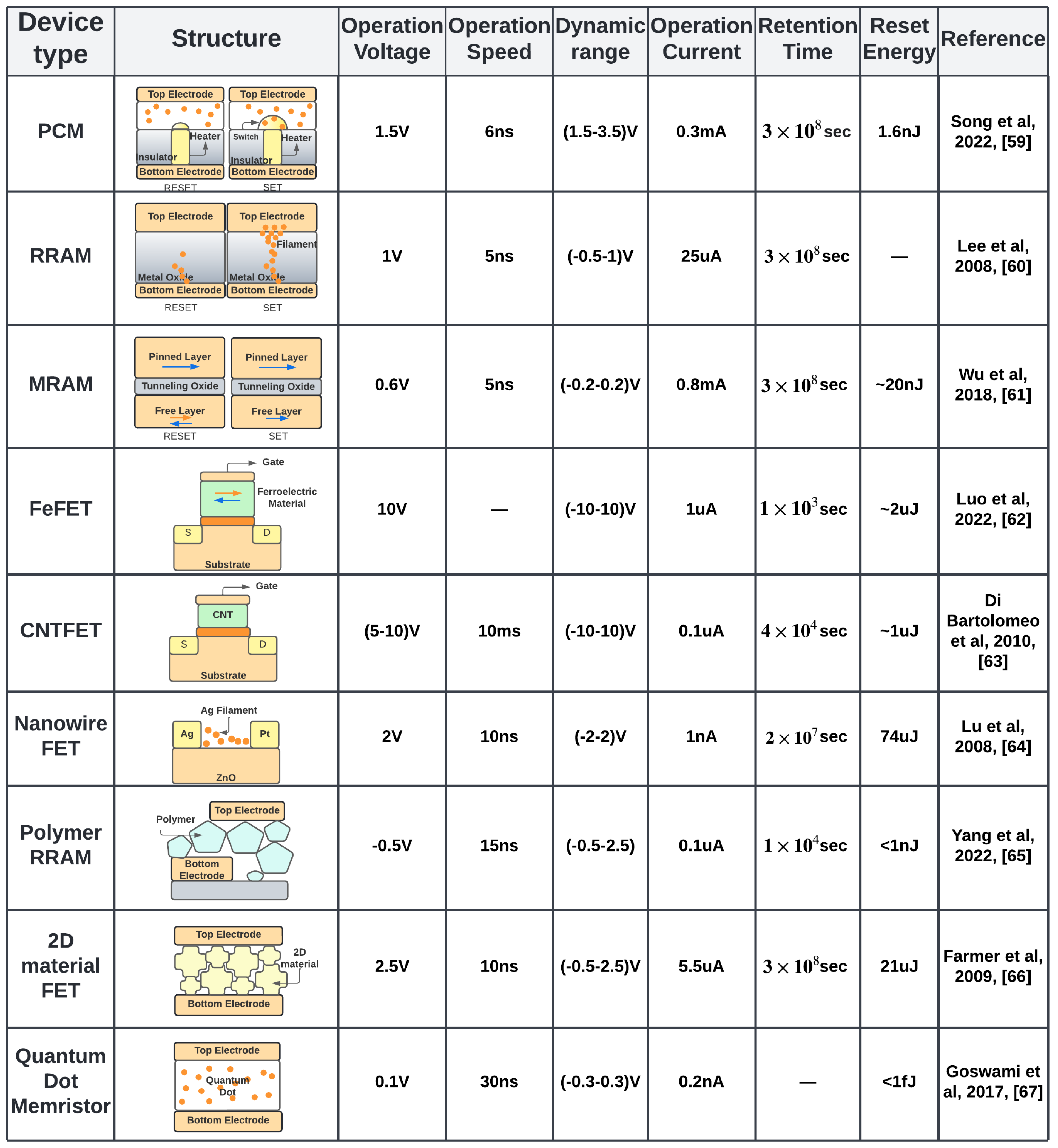
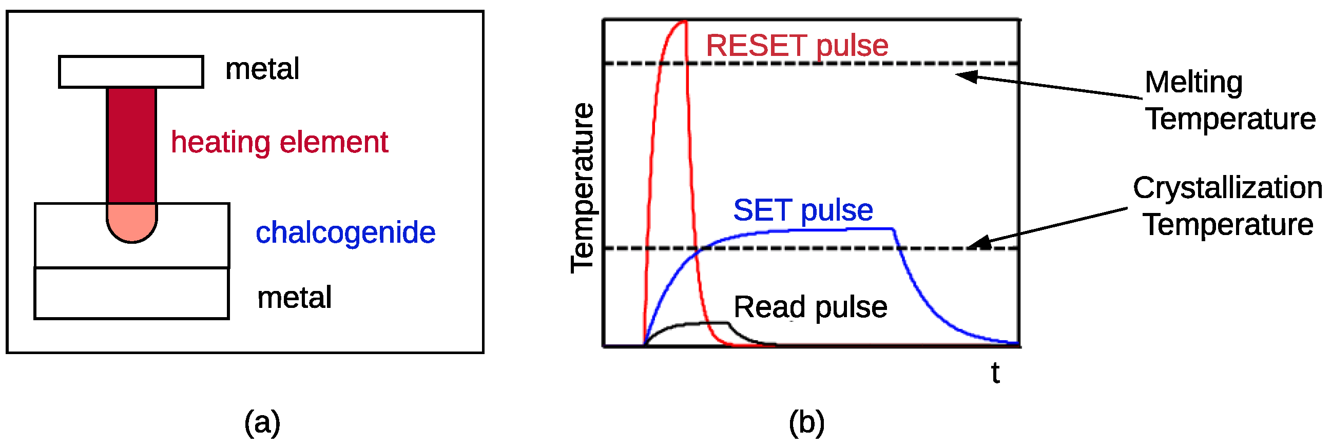

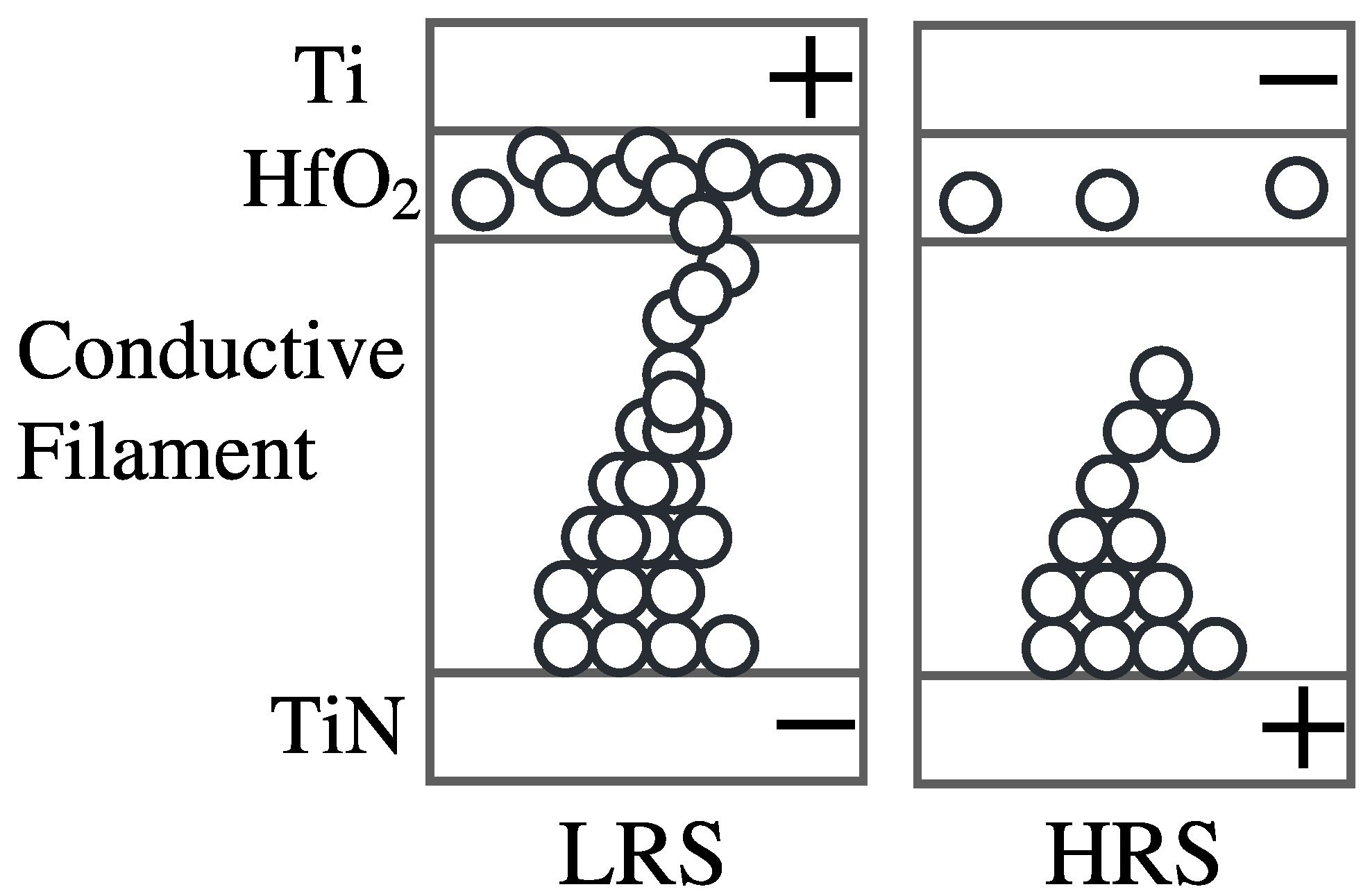
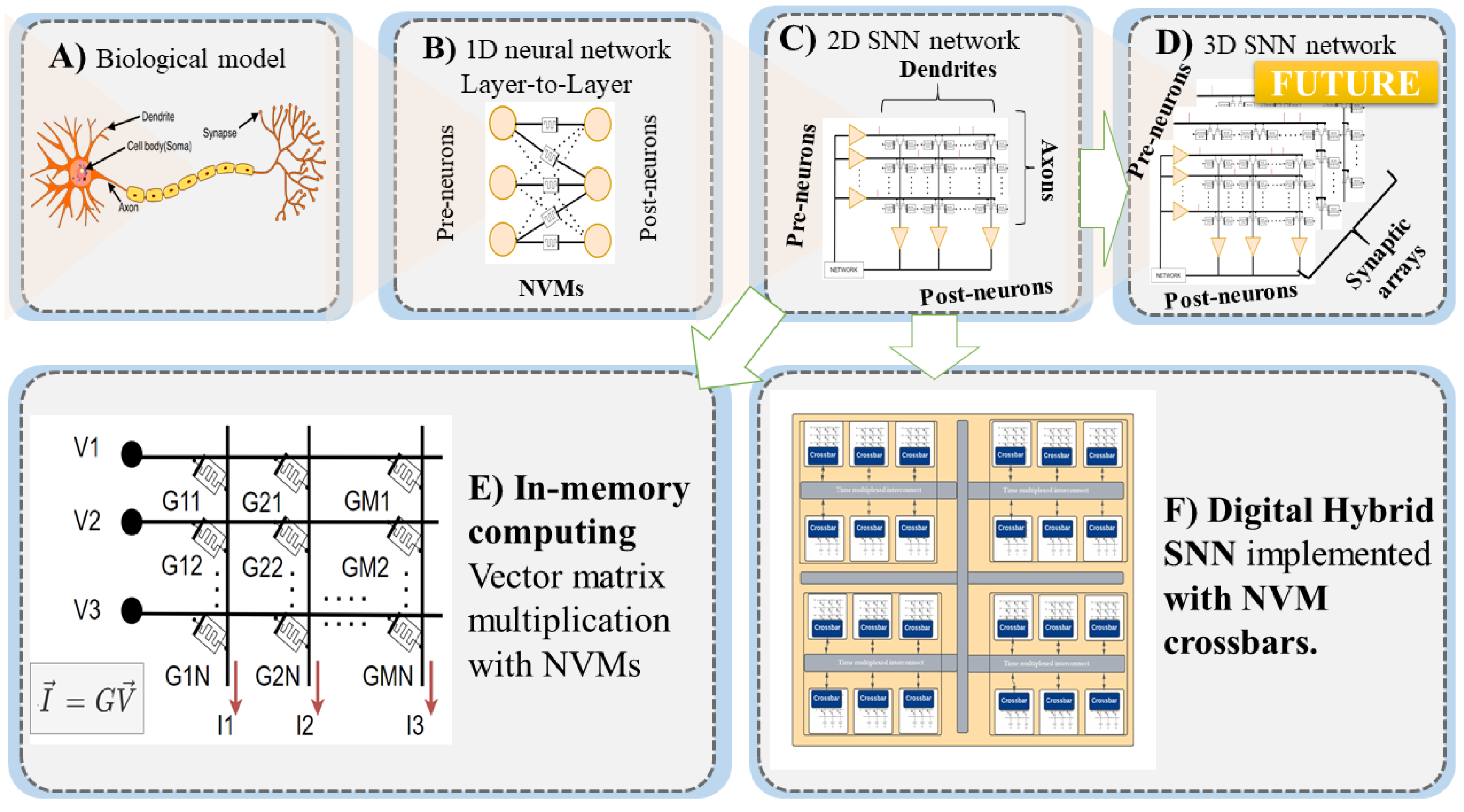
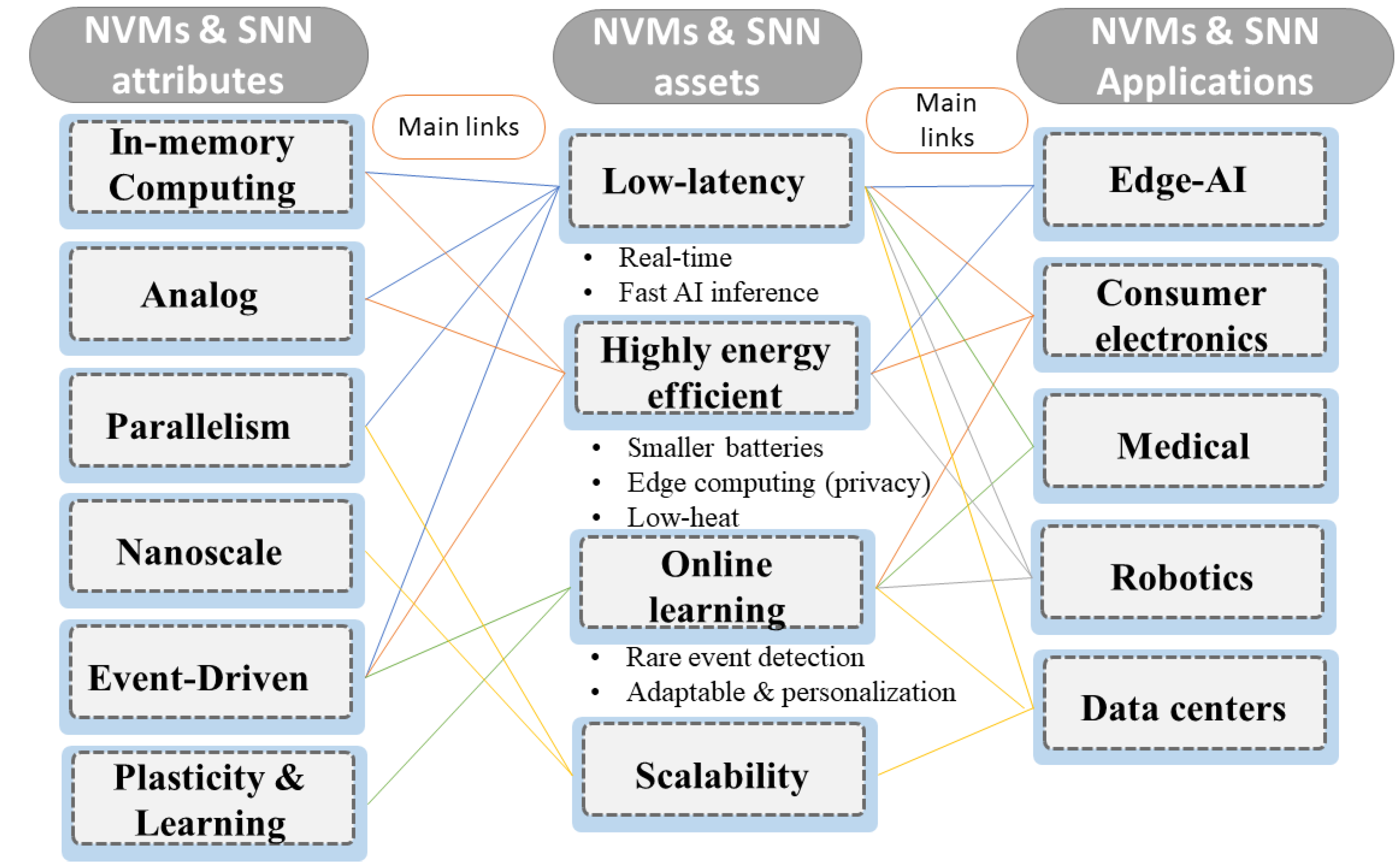
Publisher’s Note: MDPI stays neutral with regard to jurisdictional claims in published maps and institutional affiliations. |
© 2022 by the authors. Licensee MDPI, Basel, Switzerland. This article is an open access article distributed under the terms and conditions of the Creative Commons Attribution (CC BY) license (https://creativecommons.org/licenses/by/4.0/).