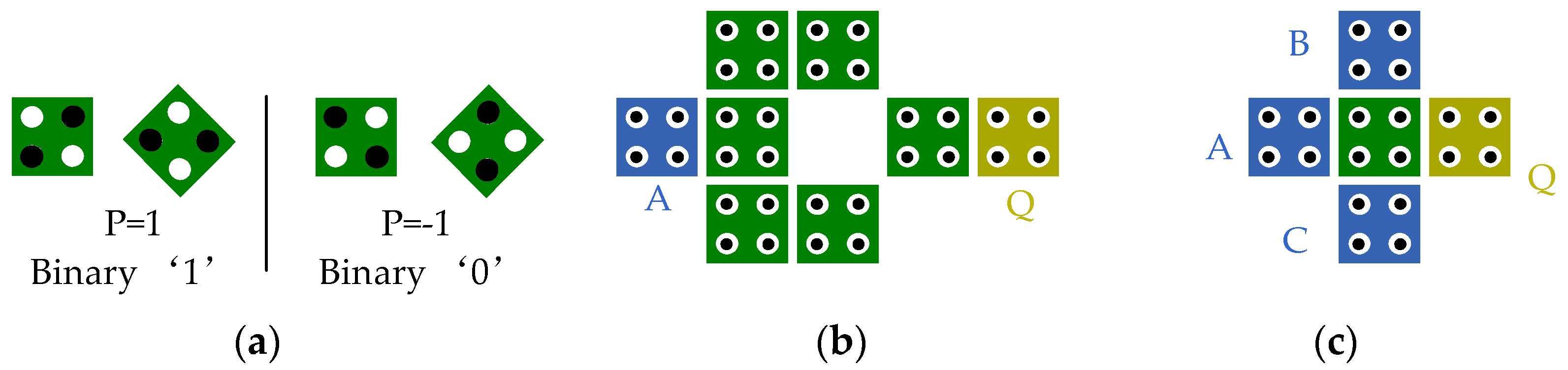
The proposed XOR/XNOR gates can be applied to the design of large QCA circuits. This section uses the proposed XOR/XNOR gates to implement level-sensitive T flip-flops (LST-FFs), negative edge-trigger T flip-flops (NET-FFs), two-to-one multiplexers, reversible gates, and (8, 4) polar encoders, respectively.
3.1. Level-Sensitive T Flip-Flops and Negative Edge-Trigger T Flip-Flops
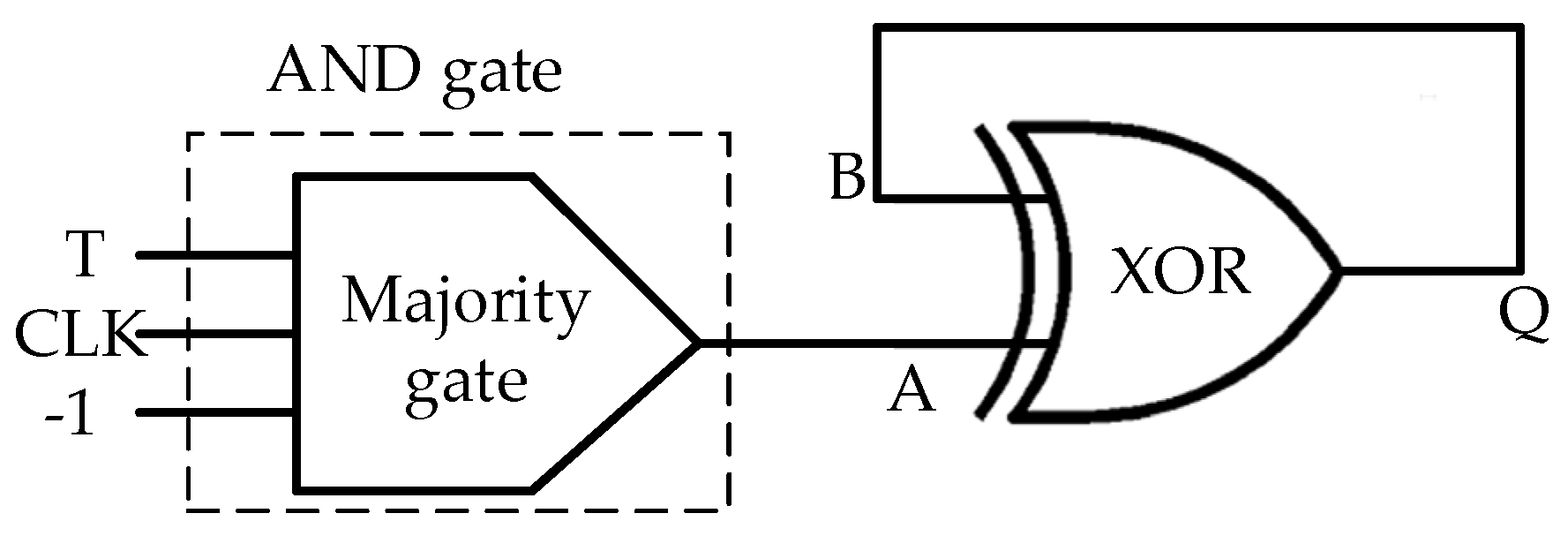
An LST-FF circuit can be implemented by using a two-input XOR gate with an AND gate [
16].
Figure 7 shows the schematic diagram of the LST-FF. An AND gate in QCA can be implemented by setting one input of the three-input majority gate to ‘−1’. The signal CLK is the clock signal of the circuit. The signal T is the input signal.
The following explains how an LST-FF works. As shown in
Figure 7, the result of the AND gate enters the input terminal A of the XOR gate, and a previous signal
is fed back to an input terminal B of the XOR gate. When signals CLK and T are ‘0’, the AND gate outputs ‘0’, and the signal enters the XOR gate to perform the XOR operation. The current output signal of the LST-FF is the same as the previous output signal (i.e., CLK = 0, T = 0,
); when signal CLK is ‘0’ and signal T is ‘1’, the AND gate outputs ‘0’, and the signal enters the XOR gate to perform the XOR operation. The current output signal of the LST-FF is the same as the previous output signal (i.e., CLK = 0, T = 1,
); when signal CLK is ‘1’ and signal T is ‘0’, the AND gate outputs ‘0’, and the signal enters the XOR gate to perform the XOR operation. The current output signal of the LST-FF is the same as the previous output signal (i.e., CLK = 1, T = 0,
); when signals T and CLK are set to ‘1’, the AND gate outputs ‘1’, and the signal enters the XOR gate to perform the XOR operation. The current output signal of the LST-FF is the complement of the previous output signal (i.e., CLK = 1, T = 1,
).
The proposed LST-FFs are sensitive to level signals.
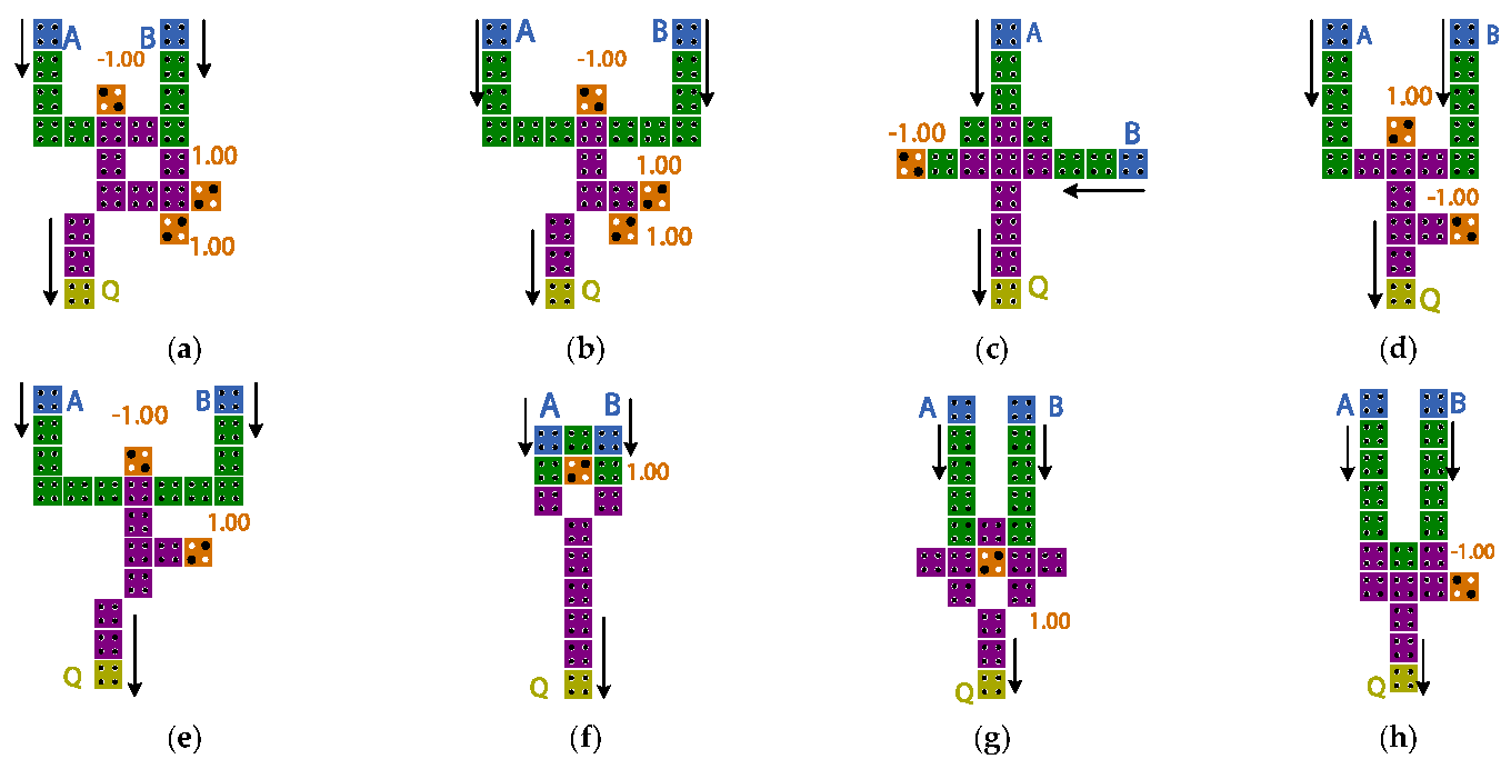
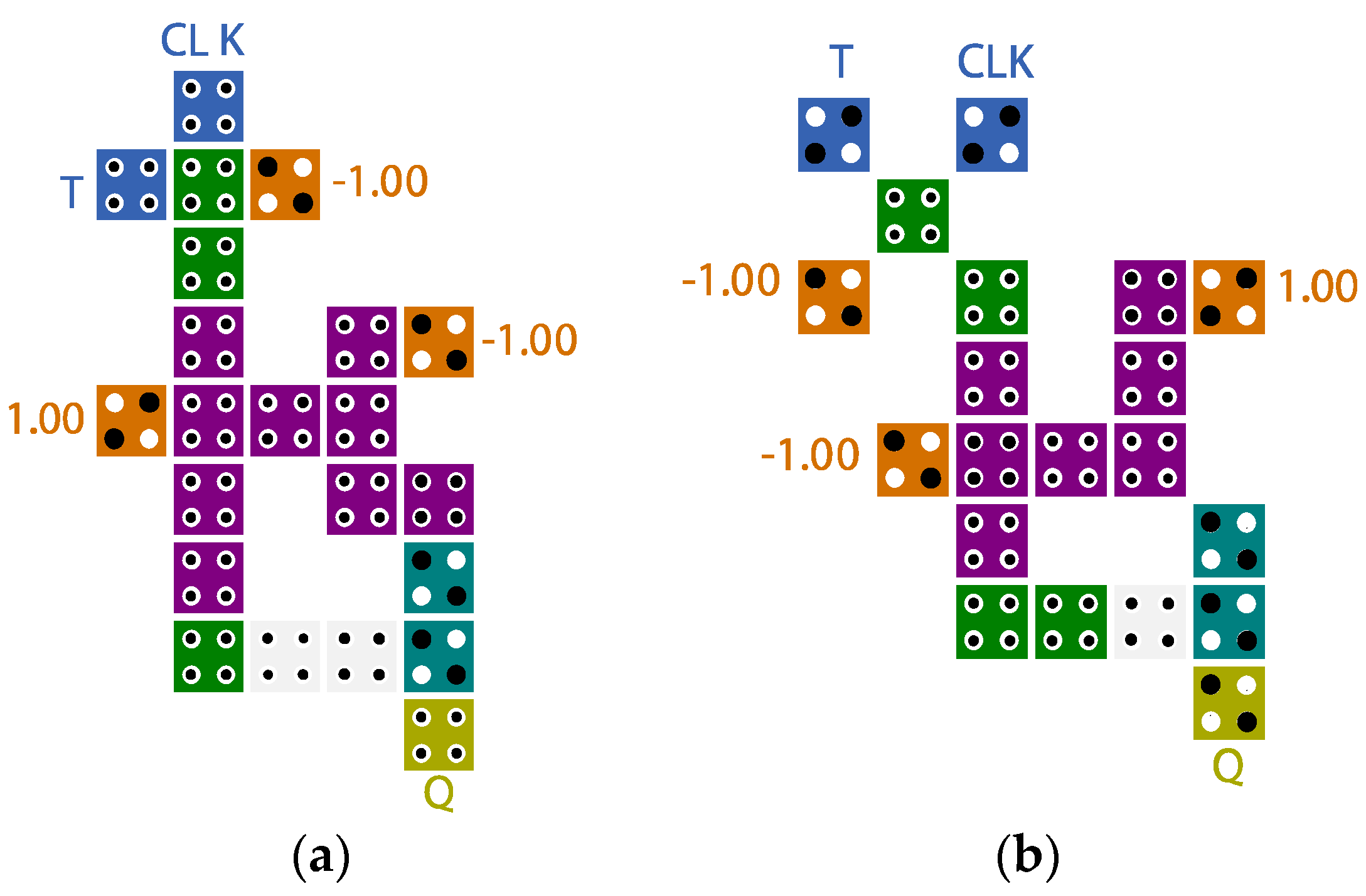
Figure 8 shows the two proposed LST-FF circuits (LST-FF1 and LST-FF2). The proposed LST-FF1 is made up of 22 cells. Its area is 17,444 nm
2 and its delay is 0.75 clock cycles. The proposed LST-FF2 is made up of 20 cells. Its area is 18644 nm
2 and its delay is 0.75 clock cycles. The designs are simulated in QCA Designer.
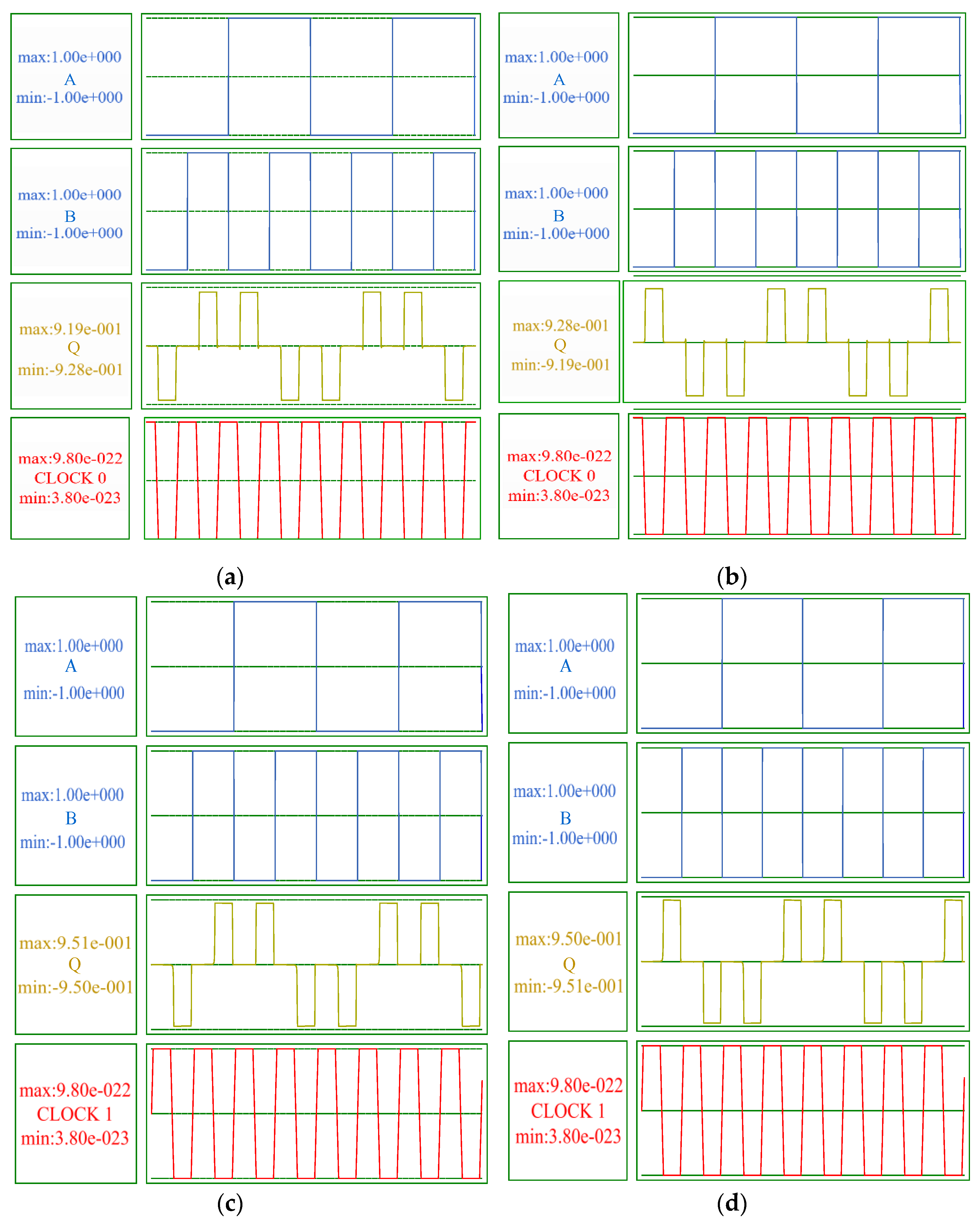
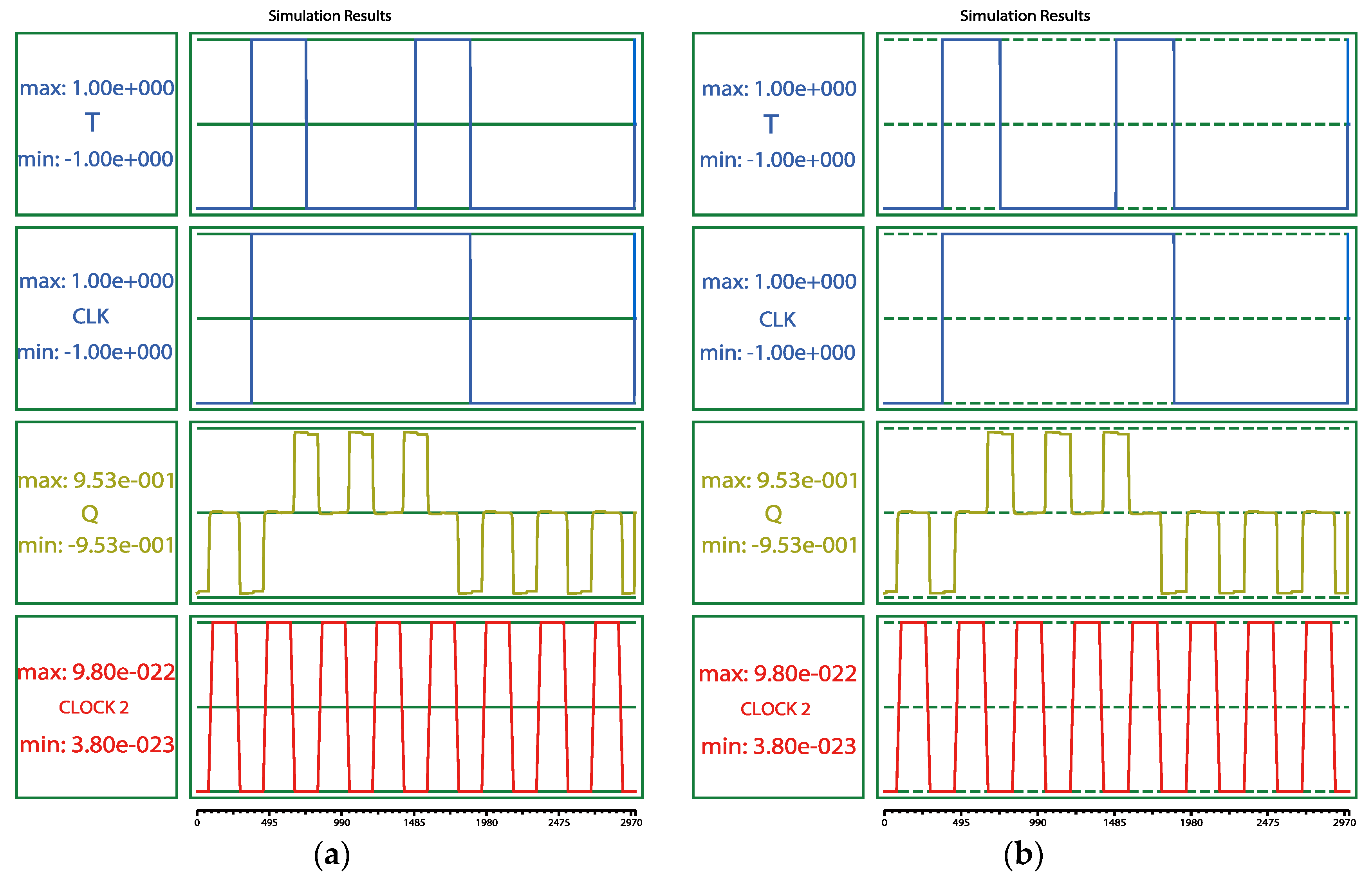
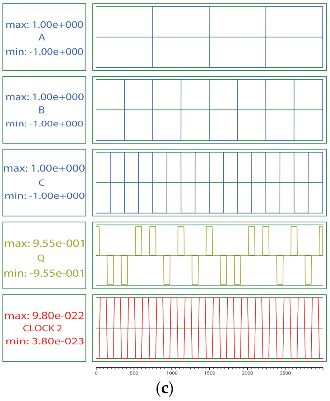
Figure 9 shows the simulation results of the LST-FF circuits. If the clock signal CLK and input signal T are both ‘1’, the current output signal is the complement of the previous output signal; otherwise, the current output signal is the same as the previous output signal.
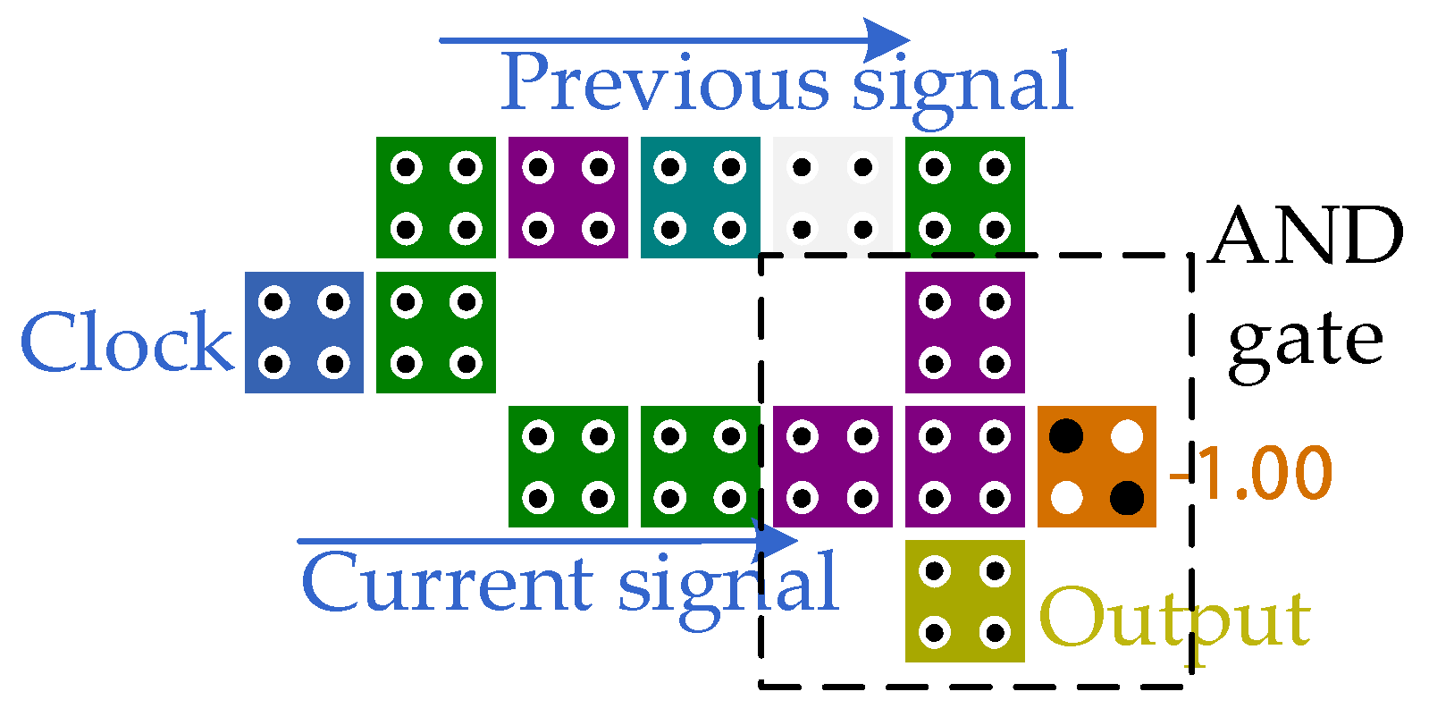
The edge-triggered T flip-flops are implemented by adding an edge detection circuit at the CLK terminal of the LST-FF. The QCA layout of the negative edge detection circuit is shown in
Figure 10 and it consists of a looped design and an AND gate [
16]. The signal clock is transmitted to two wires (previous signal and current signal). The previous signal is transmitted to an input terminal of the AND gate through a clock cycle. The current signal gets its complementary signal firstly, then it is directly transmitted to another output of the AND gate. The two signals are outputted after an AND operation. The truth table of the negative edge detection circuit is listed in
Table 4. According to the truth table, only when the signal clock changes from signal ‘1’ to ‘0’ (i.e., the negative edge is triggered), the negative edge detective circuit can output signal ‘1’, for all other changes of the signal clock, the negative edge detective circuit can output signal ‘0’.
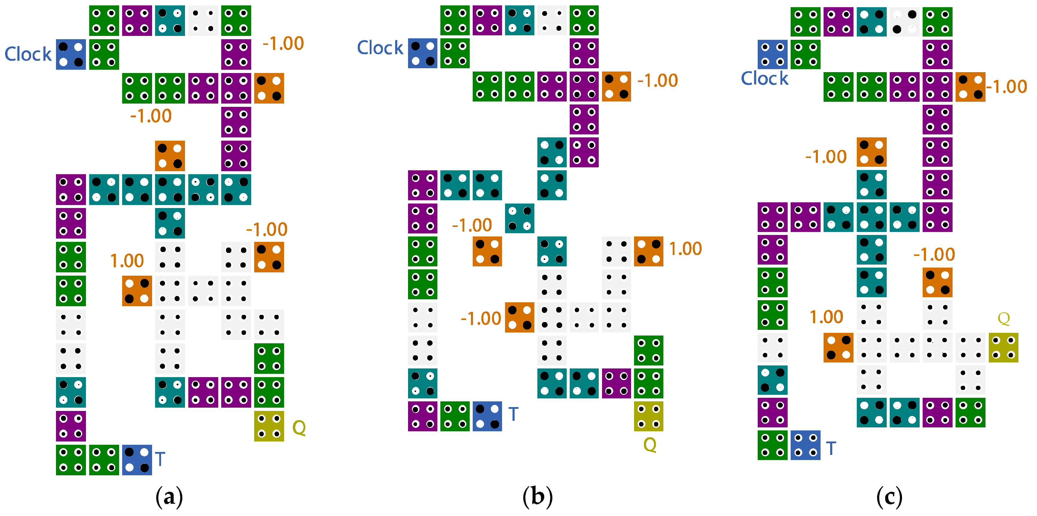
A negative edge-trigger T flip-flop (NET-FF) can be implemented by a negative edge detection circuit and an LST-FF. The negative edge detection circuit detects the changes in the signal clock, and its output state enters into the input terminal CLK of LST-FF. The specific process is as follows: When the negative edge detection circuit is triggered, a signal ‘1’ is transmitted to the CLK signal terminal of LST-FF. If the signal T is ‘1’, the output signal can be reversed; if the signal T is 0, the output signal can keep the previous output state unchanged. When the negative edge detection circuit is not triggered, a signal ‘0’ is transmitted to the input terminal CLK of the LST-FF. If the signal T is 0, the output of LST-FF remains unchanged; if the signal T is 1, the output of LST-FF remains unchanged. The three proposed NET-FFs are shown in
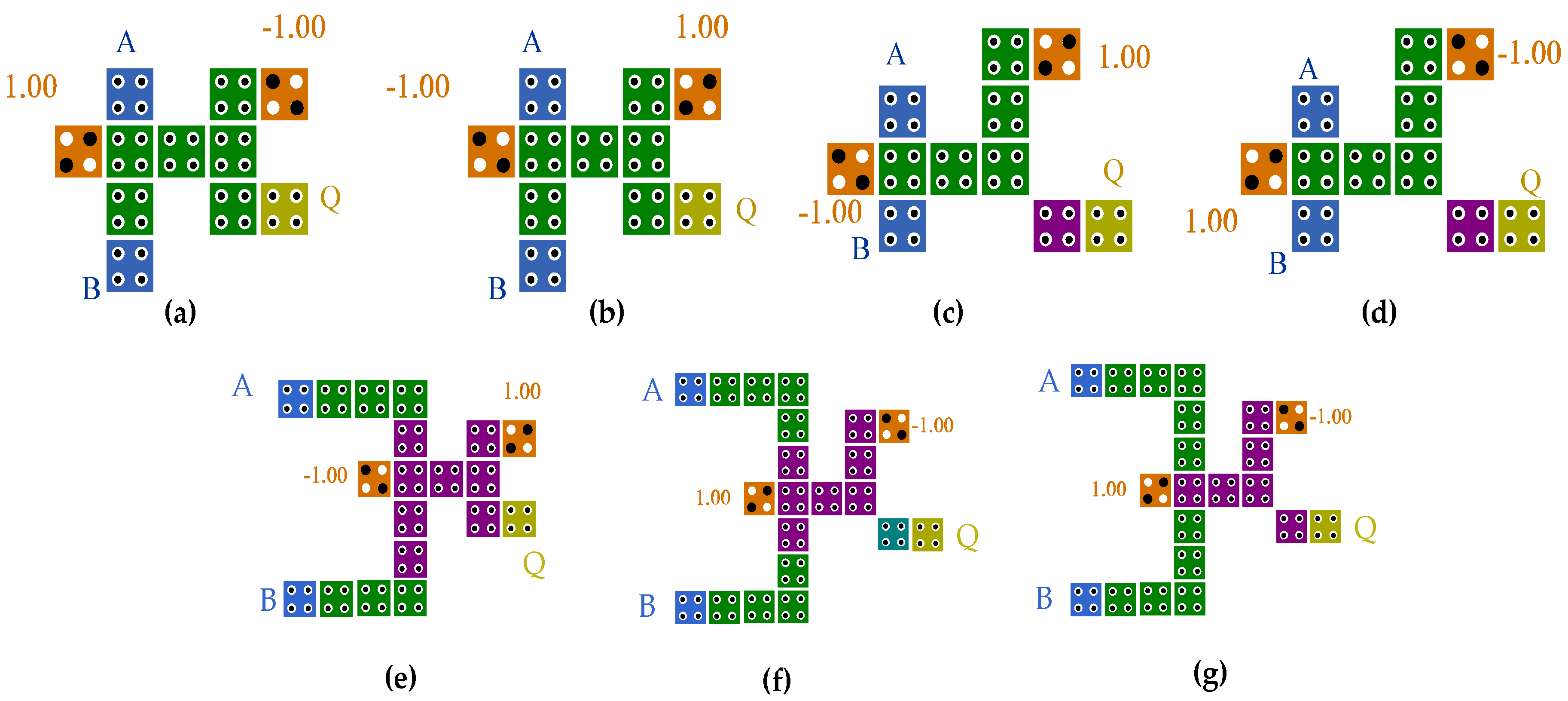
Figure 11 (NET-FF1, NET-FF2, and NET-FF3). The NET-FF3 is proposed based on the LST-FF in [
16]. The proposed NET-FF1 consists of 50 cells with an area of 38,364 nm
2 and a delay of 2.25 clock cycles. The proposed NET-FF2 consists of 47 cells with an area of 40,764 nm
2 and a delay of 2.25 clock cycles. The proposed NET-FF3 consists of 49 cells with an area of 43,924 nm
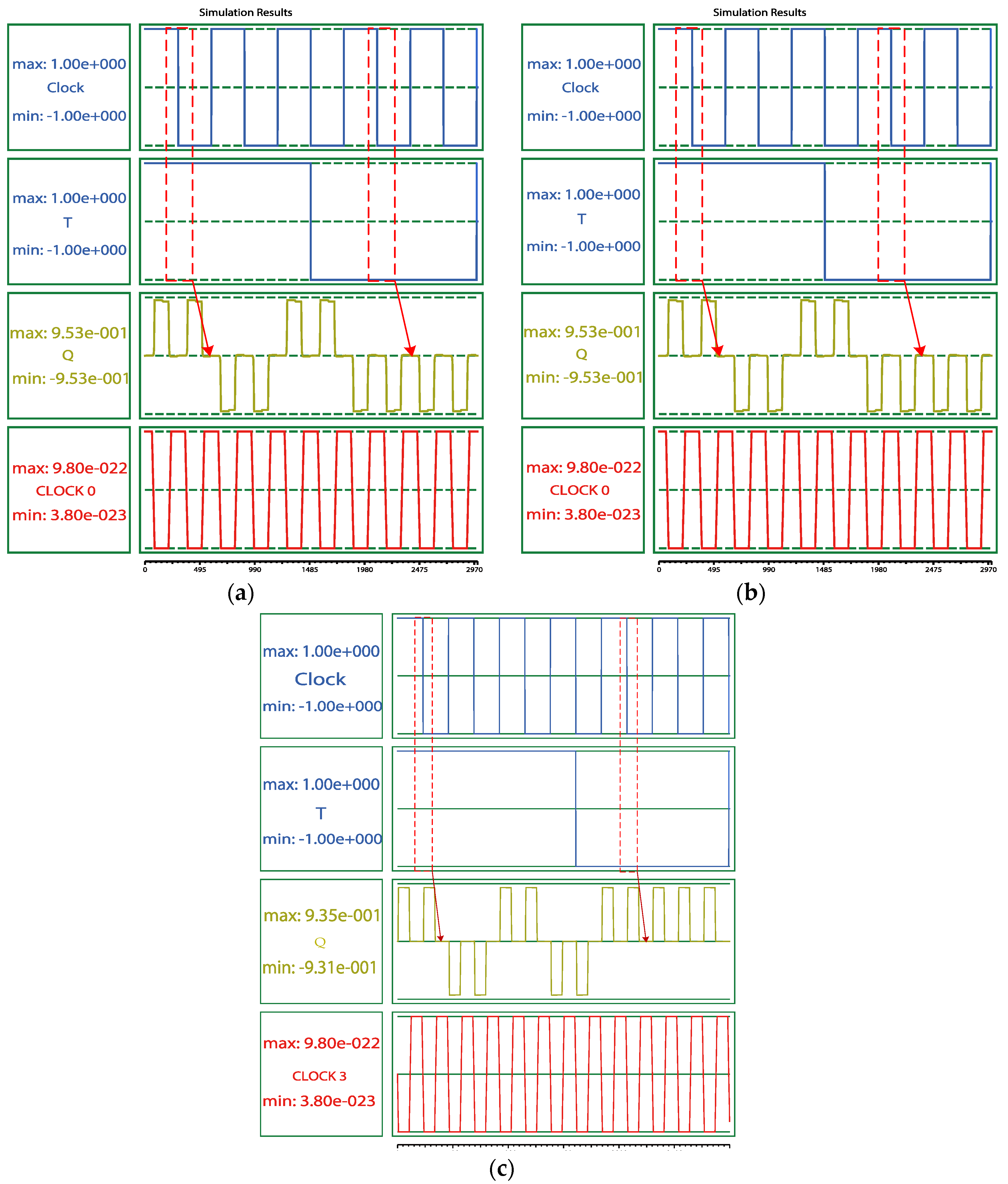
2 and a delay of 2 clock cycles. The simulation results in QCA Designer are shown in
Figure 12. For the NET-FF1 and NET-FF2, it takes 2.25 clock cycles for data to flow from inputs to output. For the NET-FF3, it takes two clock cycles for data to flow from inputs to output.
Table 5 shows the comparisons of the performance and energy consumption of the existing designs of LST-FFs and NET-FFs. It can be seen from
Table 5 that the proposed LST-FF structures are competitive in terms of cell count and area. Compared with other alternative schemes, the proposed second structure has a smaller cell count and lower power consumption. The proposed designs are lower than those designs in [
10,
11,
12,
13,
14,
15] in terms of cell count, area, delay, and power consumption. Compared with the design in [
14], the number of cells in the proposed LST-FF2 is reduced by 56.52%, the area is reduced by 66.85%, the delay is reduced by 25%, and the total energy dissipation is reduced by 60.06%. The proposed LST-FF2 uses a three-input majority gate with low fault tolerance. The second proposed design has the disadvantage of low fault tolerance. In the actual environment, the LST-FF structures should be flexibly chosen. The T-FF in [
11] does not require fixed inputs but requires two additional inputs (reset and preset inputs). The proposed LST-FFs require three fixed inputs, and the proposed NET-FFs require four fixed inputs. Xiao et al. [
35] implemented a dual-edge triggered T flip-flop. Compared with [
35], the proposed NET-FFs have a smaller cell count, smaller area, lower latency, and lower power consumption. The area of the proposed NET-FF1 is smaller than that of the proposed NET-FF2, and the energy consumption of the NET-FF2 is smaller than that of the NET-FF1. The latency of NET-FF3 based on the LST-FF proposed in [
16] is the lowest.
3.2. Two-to-One Multiplexers and Reversible Gates
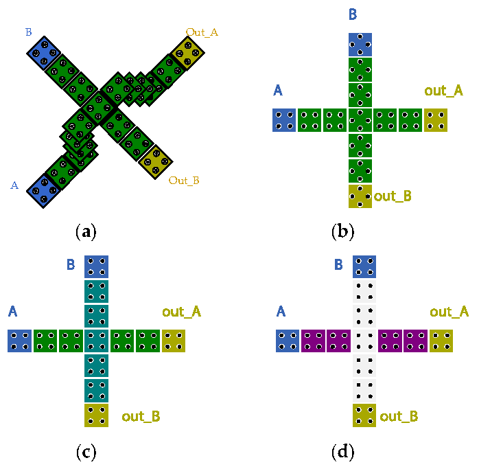
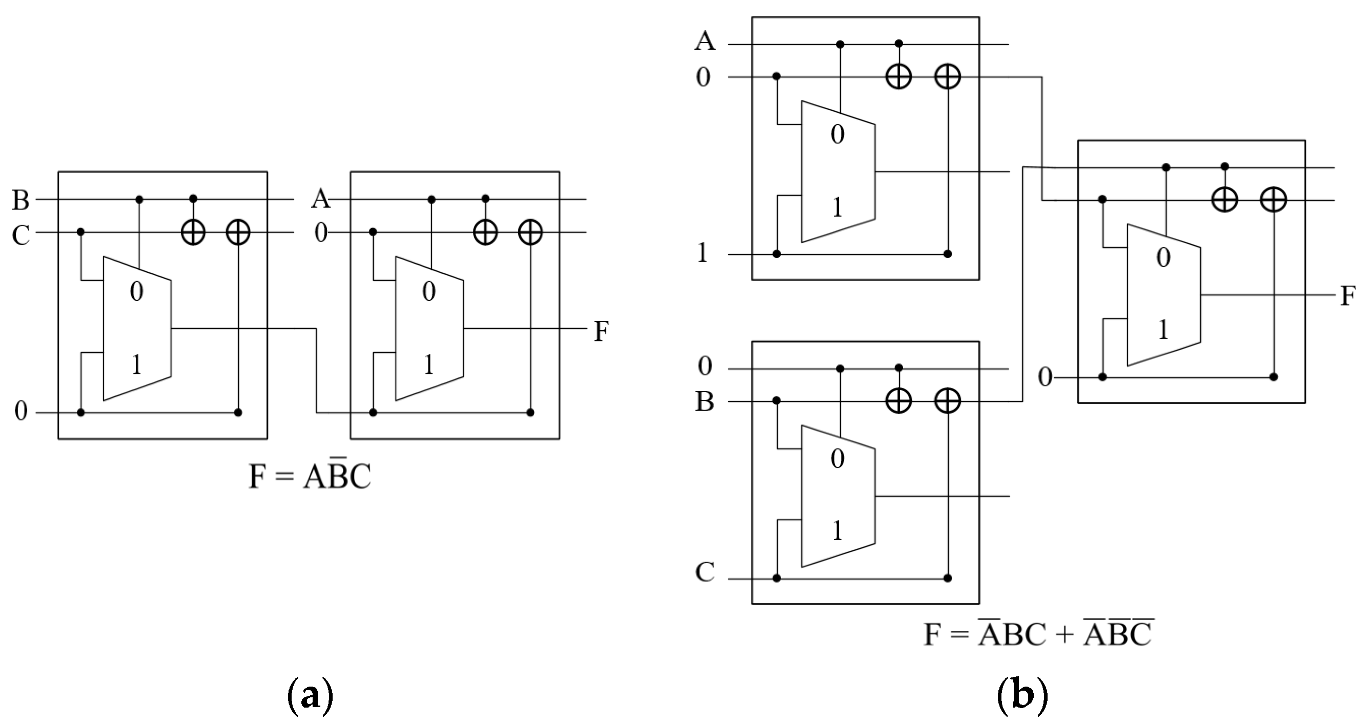
Figure 13 shows the schematic diagram of a two-to-one multiplexer [
19]. A two-to-one multiplexer can be implemented by an XOR gate and a three-input majority gate. Signals A and B perform an XOR operation to get the signal Q. Then the signals Q, B, and C enter into the three-input majority gate. Finally, the function of the two-to-one multiplexer is implemented.
Signal A is the control signal, and signals B and C are multiplexed signals. The boolean expression of the two-to-one multiplexer is derived as follows:
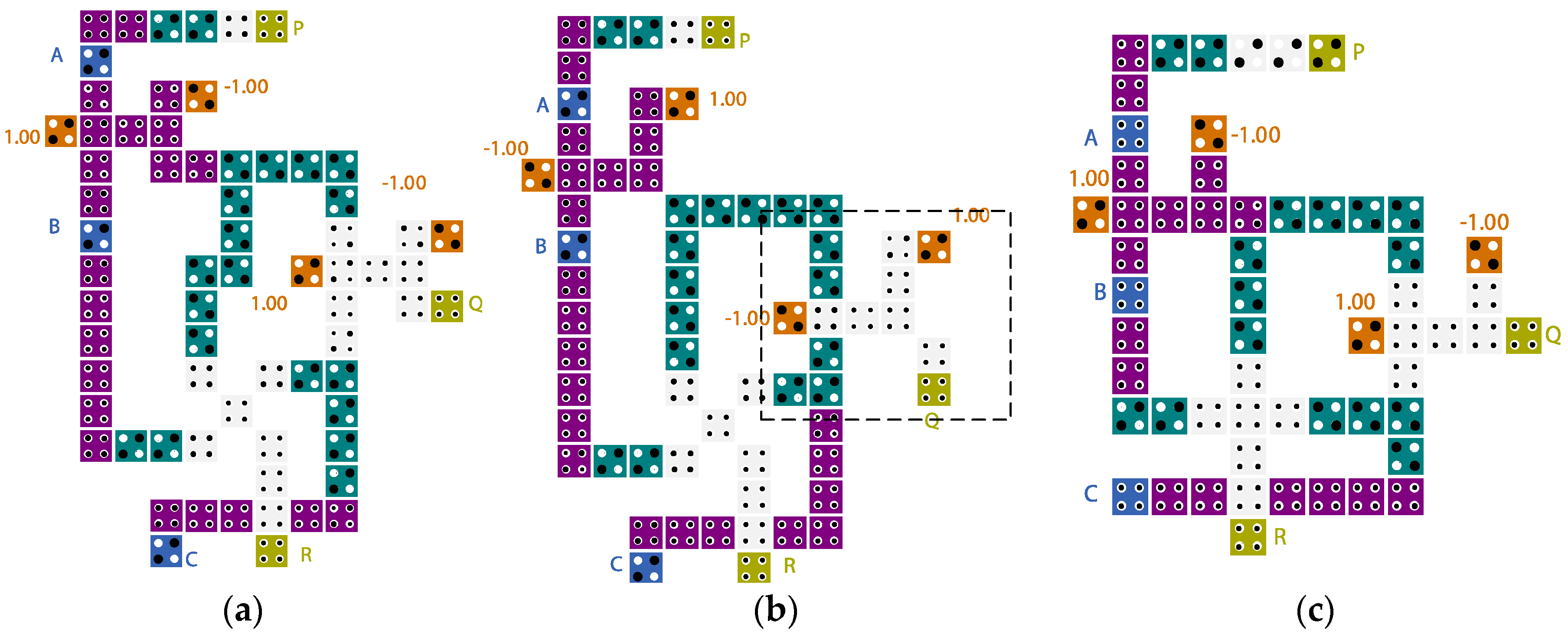
Figure 14 shows the QCA cell layouts of the proposed two-to-one multiplexers (two-to-one MUX1, two-to-one MUX2, and two-to-one MUX3). The XOR gate in the box in
Figure 14b is the proposed second XOR gate after adjusting the clock allocation. The proposed two-to-one MUX3 is based on the XOR gate in [
5]. The proposed two-to-one MUX1 consists of 25 cells with an area of 24,564 nm
2 and a delay of 0.75 clock cycles. The proposed two-to-one MUX2 is composed of 22 cells with an area of 21,804 nm
2 and a delay of 0.75 clock cycles. The proposed two-to-one MUX3 is composed of 22 cells with an area of 21,804 nm
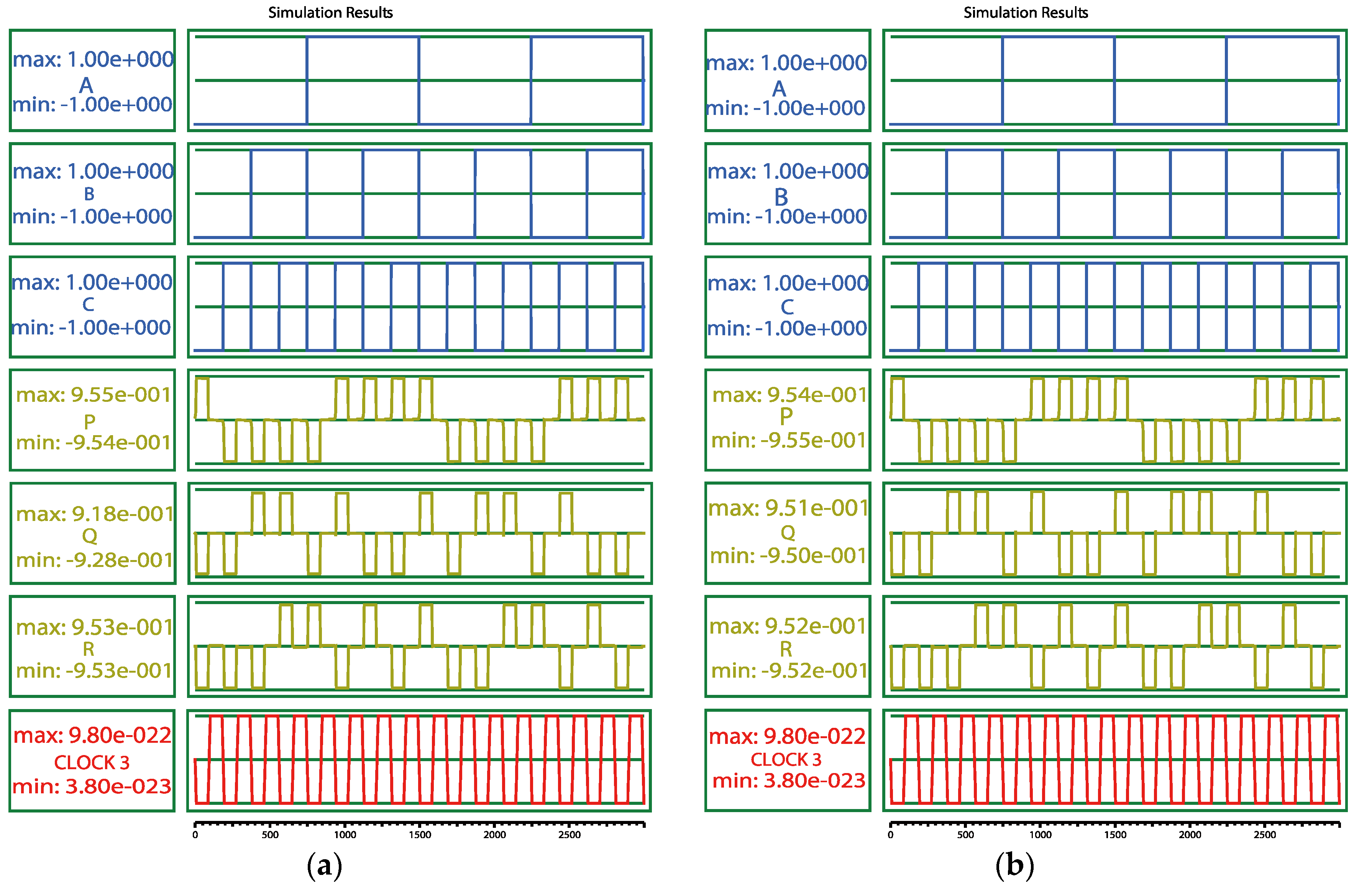
2 and a delay of 0.75 clock cycles. The proposed two-to-one multiplexers all require two fixed inputs. The designs are simulated in QCA Designer, and the simulation results are shown in
Figure 15. When the control signal A is set to ‘0’, the output signal is equal to the input value of signal B (i.e., the two-to-one multiplexer selects signal B to pass). If A is ‘1’ and the output signal is equal to the input value of signal C (i.e., the two-to-one multiplexer selects signal C to pass). It can be seen that the waveforms of the three designs in
Figure 15 are correct.
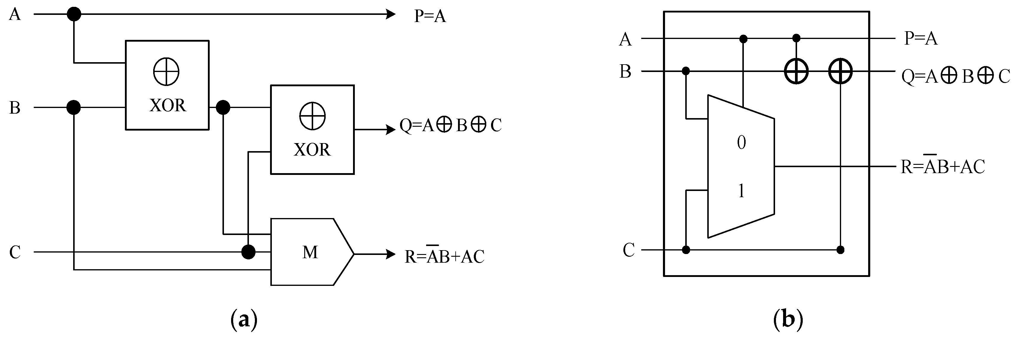
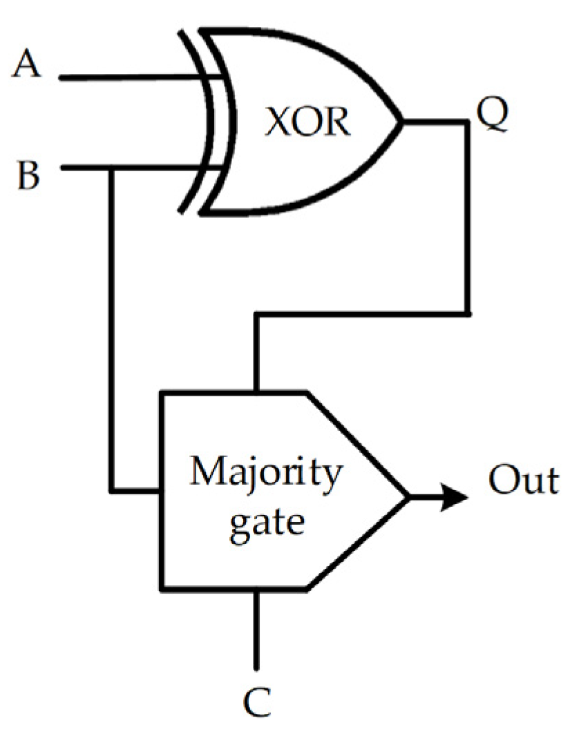
In 2017, Chabi et al. [
19] proposed a new reversible gate, and the schematic diagram is shown in
Figure 16. The reversible gate requires three inputs and obtains three outputs. The boolean expressions for the three functions are
,
, and
, respectively. The reversible gate can be used for the designs of combinatorial logic circuits. The reversible gate is composed of two XOR gates and a three-input majority gate. The output terminal P is equal to the value of the input signal A. The signal A is directly transmitted to the output terminal P through a wire.
The implementation of output terminal Q is as follows. As shown in
Figure 16, signals A and B are transmitted to the first XOR gate for an XOR operation. Then the result and signal C are transmitted to the second XOR gate to implement the XOR operation of the three signals.
The output terminal R implemented the function of the two-to-one multiplexer. The terminal R’s function is implemented by an XOR gate and a three-input majority gate. Signal A is the control signal and B and C are two multiplexed signals. When signal A is low-voltage, signal B is transmitted to the output terminal; when signal A is high-voltage, signal C is transmitted to the output terminal.
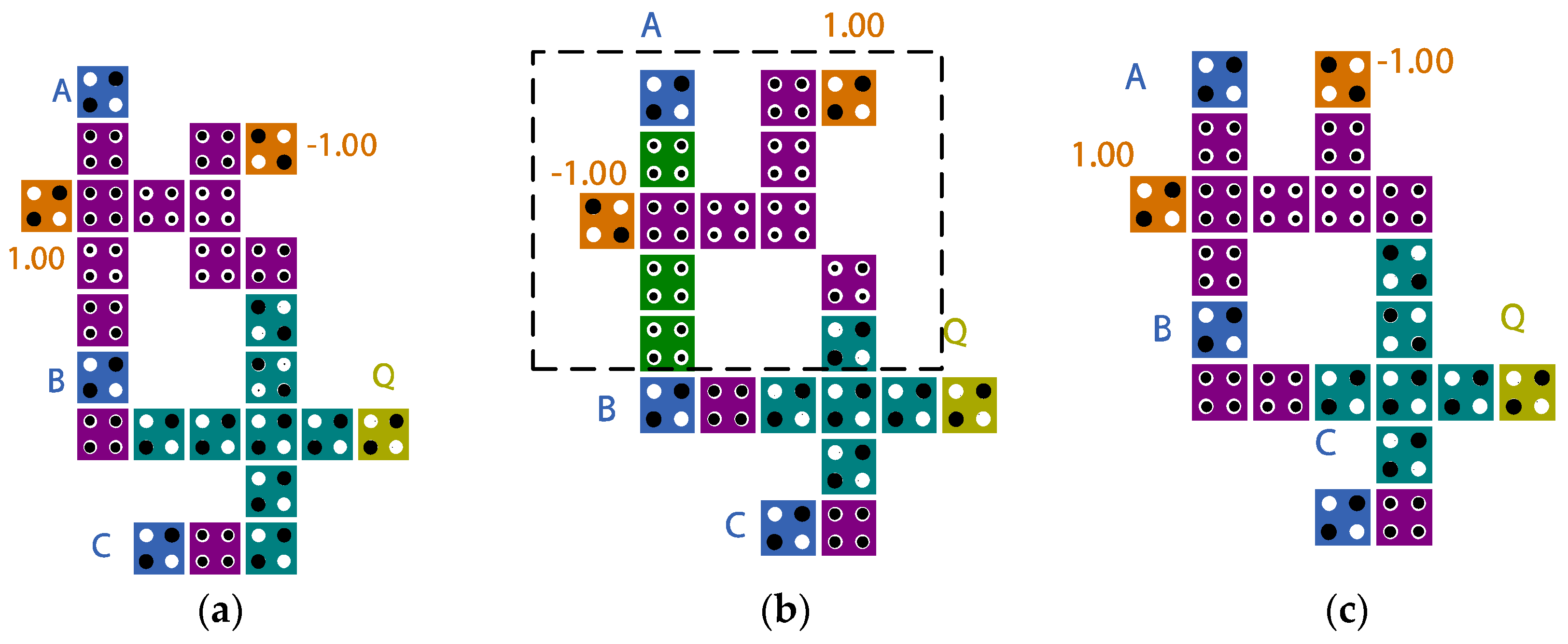
Figure 17 shows the QCA cell layouts of the proposed reversible gates (RG1, RG2, and RG3). The RG3 is implemented by using an existing XOR in [
5]. The XOR gate in the box in
Figure 17b is the proposed second XOR gate after adjusting the clock allocation which reduces a delay of 0.25 clock cycles. The proposed RG1 gate consists of 68 cells with an area of 0.08 µm
2 and a delay of one clock cycle. The proposed RG2 gate consists of 65 cells with an area of 0.08 µm
2 and a delay of one clock cycle. The proposed RG3 gate consists of 57 cells with an area of 0.06 µm
2 and a delay of one clock cycle. The proposed reversible gates all require four fixed inputs. The designs are simulated in QCA Designer.
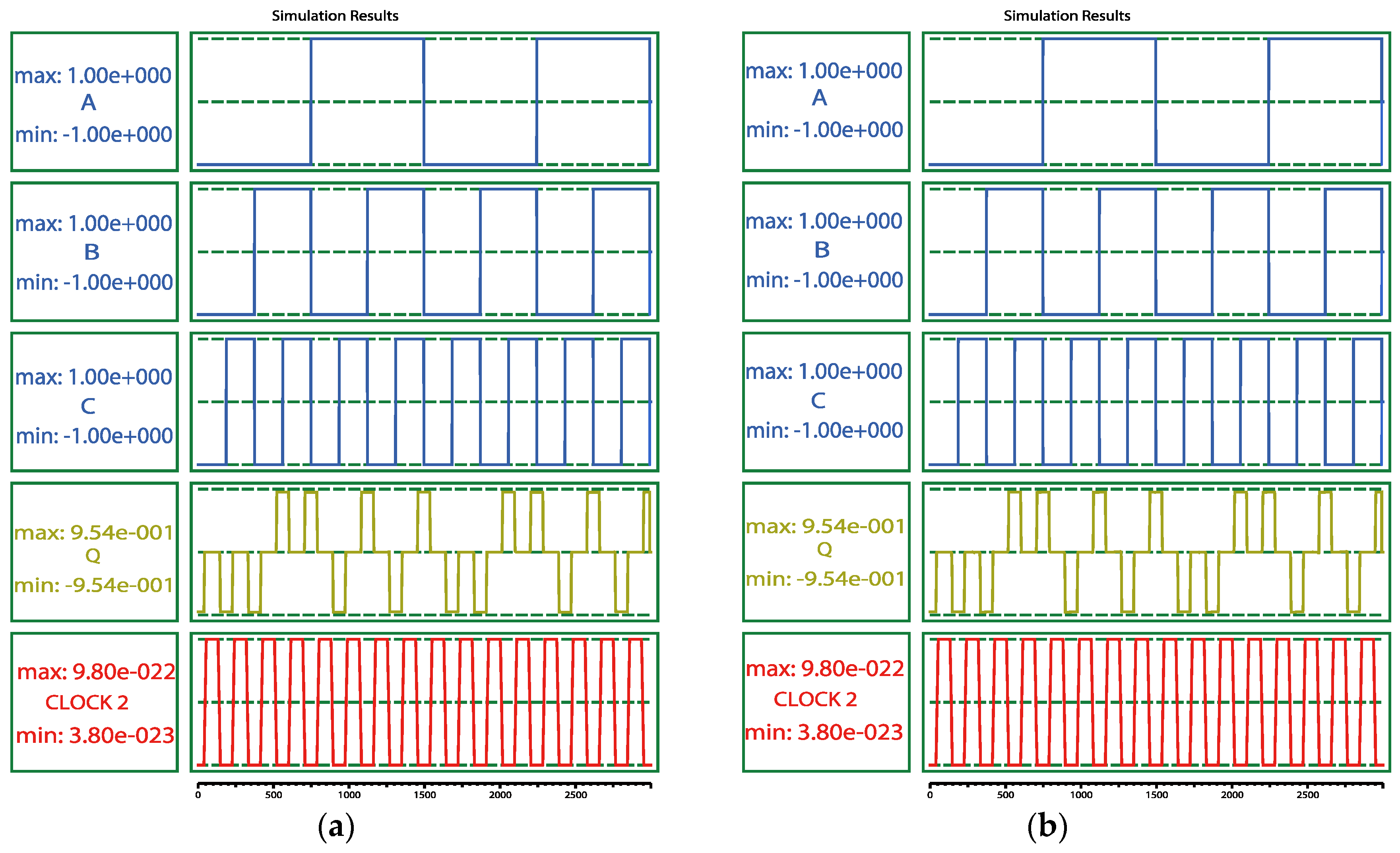
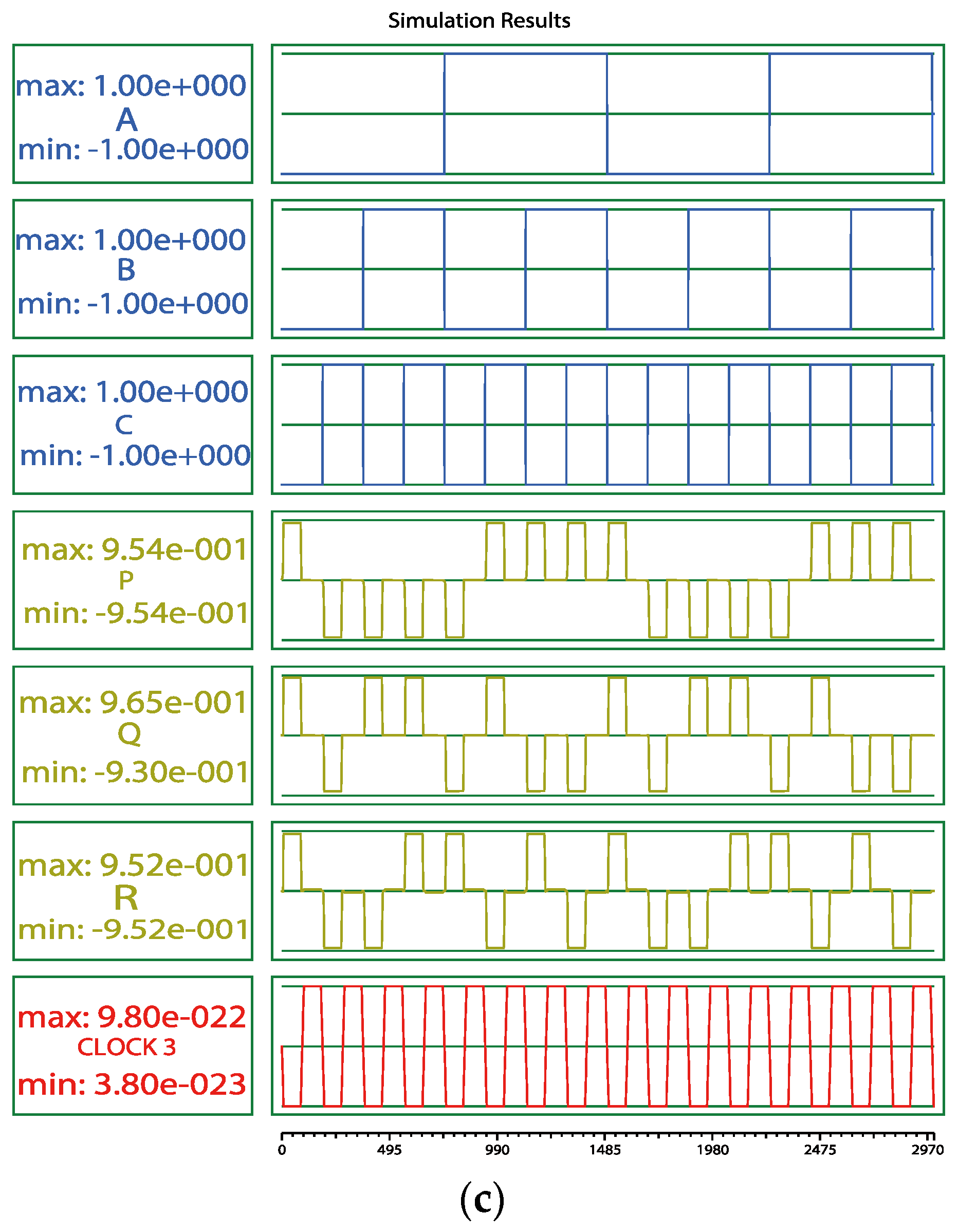
Figure 18 shows the simulation results of three proposed reversible gates. It can be seen that the waveforms of the three designs in
Figure 18 are correct.
The reversible gate can be used to design large combinatorial logic circuits based on boolean functions. Two logic functions are given in
Figure 19. The
can be implemented by the two reversible gates and the
can be implemented by the three reversible gates. Other boolean functions can also be constructed by this reversible gate.
Table 6 shows the comparisons among the existing two-to-one multiplexers. It can be seen from
Table 6 that the proposed two-to-one multiplexers have fewer cells compared with [
17,
18].
Table 7 shows the comparisons between the existing reversible gates. Compared with [
19], the cell count and area of the proposed RG1 are reduced by 24.44% and 11.11%, respectively; the cell count and area of the proposed RG2 are reduced by 27.78% and 11.11%, respectively. It can be seen from
Table 7 that the cell count and area of the third reversible gate designed using the XOR gate in [
5] are the smallest.
Table 8 shows the energy consumption comparisons of alternative two-to-one multiplexers and reversible gates. Only the power consumption of the single-layer designs is considered. It can be seen that the design in [
20] is optimal. However, the three-input majority gates of the multiplexer in [
20] have low fault tolerance. As can be seen from
Table 8, the energy consumption of the proposed two-to-one MUX2 is lower than that design of [
19]. The proposed reversible gates are an improvement of the design in [
19]. Compared with the energy consumption of the design in [
19], the power consumption of the proposed RG2 is lower. The power consumption of the proposed RG1 is higher than that of the design in [
19].
3.3. Polar Encoders
In secure communications, encoders and decoders can be implemented by using QCA circuits. Polar code was initially introduced by E. Arikan in 2009 [
36]. Polar code is a forward error correction code used for signal transmission. Polar code has explicit proof for the channel performance which has now almost closed the gap to Shannon’s limit and is included as code for the control channels in the 5G standard.
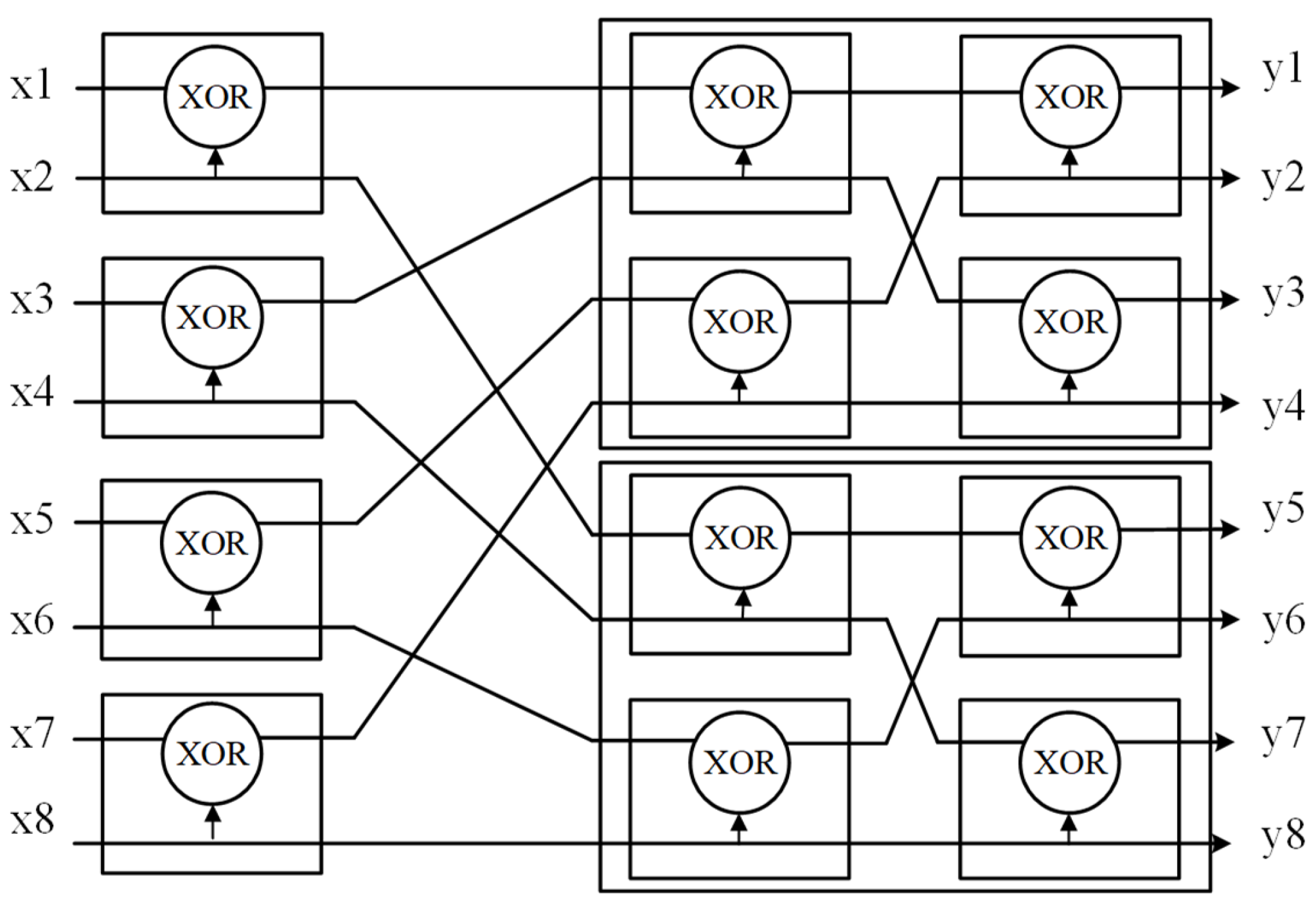
Figure 20 shows the design of polar encoders in the QCA technology proposed by Das et al. [
27]. If the inputs x1, x2, x3, and x5 in
Figure 20 are set to ‘0’, it can act as an (8, 4) polar encoder (G(8, 4)). Formulas (4)–(11) are boolean expressions for the eight outputs of G(8, 4).
We propose and have implemented the two coplanar G(8, 4) circuits using two proposed XOR gates.
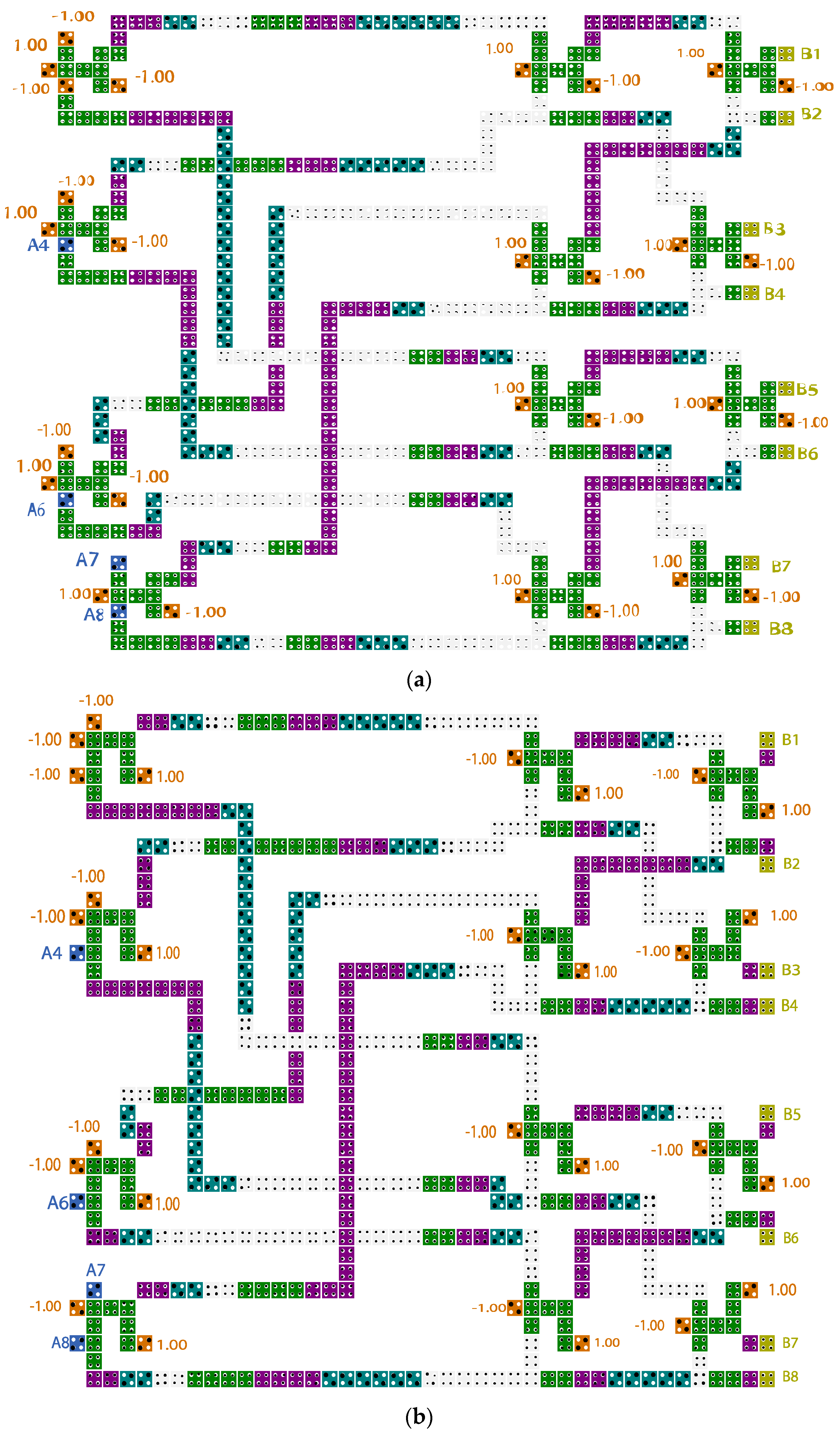
Figure 21 shows the layouts of the two proposed G(8, 4) designs.
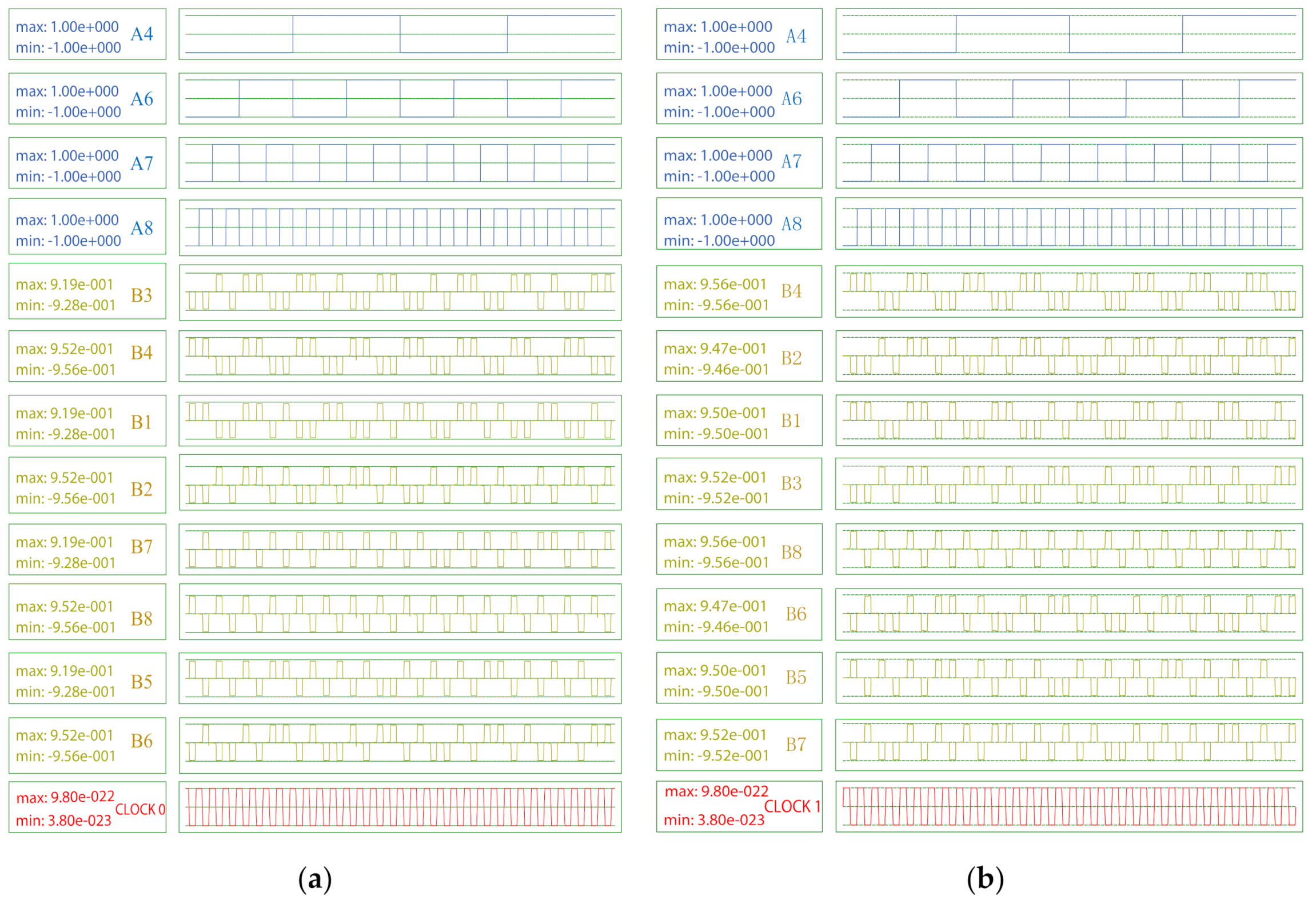
Figure 22 shows the simulation results of the G(8, 4) designs in QCA Designer. The simulation engine of QCA Designer was set to the coherence vector engine, the total simulation time was set to 7.000000e-010 s, and other parameters were set to the default values. The first proposed G(8, 4) consists of 524 cells (see
Figure 21a). Its area is 0.685 µm
2 and its latency is 3.25 clock cycles. The total and the average energy dissipation of the first proposed G(8, 4) is 1.31 × 10
−1 eV and 1.19 × 10
−2 eV. The second proposed G(8, 4) consists of 518 cells (see
Figure 21b). Its area is 0.635 µm
2 and its latency is 3.50 clock cycles. The total and average energy dissipation of the second proposed G(8, 4) are 1.08 × 10
−1 eV and 9.84 × 10
−3 eV.
Table 9 shows the comparisons of the performance and energy consumption of the two proposed G(8, 4) circuits. The cell count, area, and latency of the proposed G(8, 4) circuits are lower compared with alternative solutions and the second proposed G(8, 4) has the lowest energy dissipation. The two proposed G(8, 4) designs have more external fixed inputs than the design in [
28]. In the future, the method proposed by Khosroshahy et al. in [
25] can be applied to reduce external fixed inputs of the proposed G(8, 4) designs. Compared with the best solution in [
28], the cell count and area of the second proposed G(8, 4) are reduced by 13.67% and 12.05%, respectively, and the latency is reduced by 0.25 clock cycles. Therefore, the two proposed (8, 4) polar encoders, especially the second one, are competitive in terms of cell count, area, and energy consumption.


