Abstract
A chiplet placement algorithm for 2.5-D IC integration on an interposer is discussed in this paper. Inspired by the NoC (network-on-chip) mapping problem, we propose a novel chiplet placement algorithm called the CCEOA (chiplet communication energy optimization algorithm), which takes into account the actual size of the chiplet. The CCEOA can map chiplets to mesh topology, resulting in a layout with a low CEC (communication energy consumption). The algorithm considers the spacing of the chiplets while selecting the initial nodes and the nodes to map the next chiplet. Furthermore, because there exist nodes resulting in the same CEC increment during the mapping process, the algorithm adopts a secondary local exploration strategy to further select nodes. Meanwhile, the lateral and vertical placements of chiplets are also considered. The algorithm is implemented and evaluated with a 2.5-D IC integration with 22 chiplets to demonstrate its efficiency and the accuracy.
1. Introduction
Traditional monolithic 2D integrated chip (IC) designs are increasingly having difficulty following Moore’s law, as semiconductor technology advances and the design complexity of system-on-chip (SoC) increases [1]. Printed circuit boards (PCBs) have traditionally been utilized as integration platforms. PCBs are mature and cost-effective, but their lengthy and wide traces cause a high inductance and capacitance, restricted bandwidth and substantial power losses [2,3]. As a result, interposer-based 2.5-D IC integration has received a lot of interest as a way to overcome the constraints of 2-D IC integrations [4,5]. Based on an interposer, 2.5-D IC integration separates a single SoC into numerous functional blocks known as chiplets, which are placed side-by-side on the interposer and coupled with high speed and bandwidth through the interposer. This approach significantly reduces the design cycle, complexity and cost. It enables the heterogeneity of blocks in multiple technologies and permits the reuse of off-the-shelf intellectual properties (IPs) [6,7]. Instead of redesigning the entire system, SoC designers can replace only the necessary chiplets. Because the known good dies (KGDs) are picked as chiplets, the development risk of SoC in 2.5-D integration is reduced much more than that of a traditional 2-D IC design [8]. Furthermore, Intel’s FOVEROS technology and AMD’s Zen 2 microarchitecture show that 2.5-D IC technology is no longer an option but rather a new trend in the system-on-chip (SoC) design.
The speed of the semiconductor development is increasing as a result of fifth-generation (5G technology standard for broadband cellular networks) and artificial intelligence (AI) [9]. While 2.5-D IC integration provides a higher level of integration, the smaller physical size and spacing of the interconnects lead to increased coupling effects and interference between the interconnects, which pose a challenge to chiplet communication issues. A reasonable layout would improve the chiplet communication.
The advancement of chip technology has resulted in ongoing advancements in packaging technologies. Kim et al. presented an effective methodology for the co-design, co-analysis and the system-level optimization of the chiplet/interposer power network (PDN) in 2.5-D IC integration [10]. Kabir et al. proposed a chip-package co-design flow for 2.5-D IC integration. Their flow included 2.5-D-aware partitioning suitable for SoC design, chip-package floor planning, post-design analysis and the verification of the entire 2.5-D IC integration [11]. Park et al. presented a complete EDA flow and design strategies targeting active interposer-based 2.5-D IC integration. They concentrated on the co-analysis of power, performance, signal and power integrity, the related co-optimization of chiplets and the active interposer [12].
Various chiplet placements result in different CECs. It is crucial to figure out how the chiplets should be arranged. Various heuristic techniques have been used to handle similar problems in NoC. Murali, S. et al. presented NMAP, which was a fast algorithm that mapped the cores onto a mesh NoC architecture under bandwidth constraints, thus, minimizing the average communication delay [13]. Wang et al. proposed a new effective optimization method based on the discrete particle swarm optimization framework, including the novel principles for representation, velocity computing and position-updating of the particles [14]. Liu et al. proposed a multi-objective ant colony algorithm (MOACA) that mapped IP cores onto mesh-based NoC architectures, which showed to be an efficient way of finding the pareto-optimal front-optimizing energy consumption and hotspot temperature of an NoC [15].
In this article, we propose a heuristic algorithm, the CCEOA (chiplet communication energy optimization algorithm), based on the 2D NoC mapping algorithm SYMMAP (symmetry mapping) [16] to discover a feasible layout of 2.5-D IC integration for a low CEC, considering the peculiarities (actual size, chiplet space, etc.) of 2.5-D IC integration.
2. Model Establishment
Mesh topology is used in mapping. Standard NoC mapping only considers that one IP core occupies one node in topology, but this is not the case in 2.5-D IC integration. Because the chiplets are different sizes, we should take the area factor into account. At the same time, the distance between the chiplets would be different if the chiplets were placed horizontally or vertically. To solve these problems, we needed the following novel models.
2.1. The 2.5-D IC Integration Mapping Model
In this study, a 2.5-D IC integration with 22 chiplets was used as an example. The model consisted of an FPGA, Memory, AD, DA, etc.
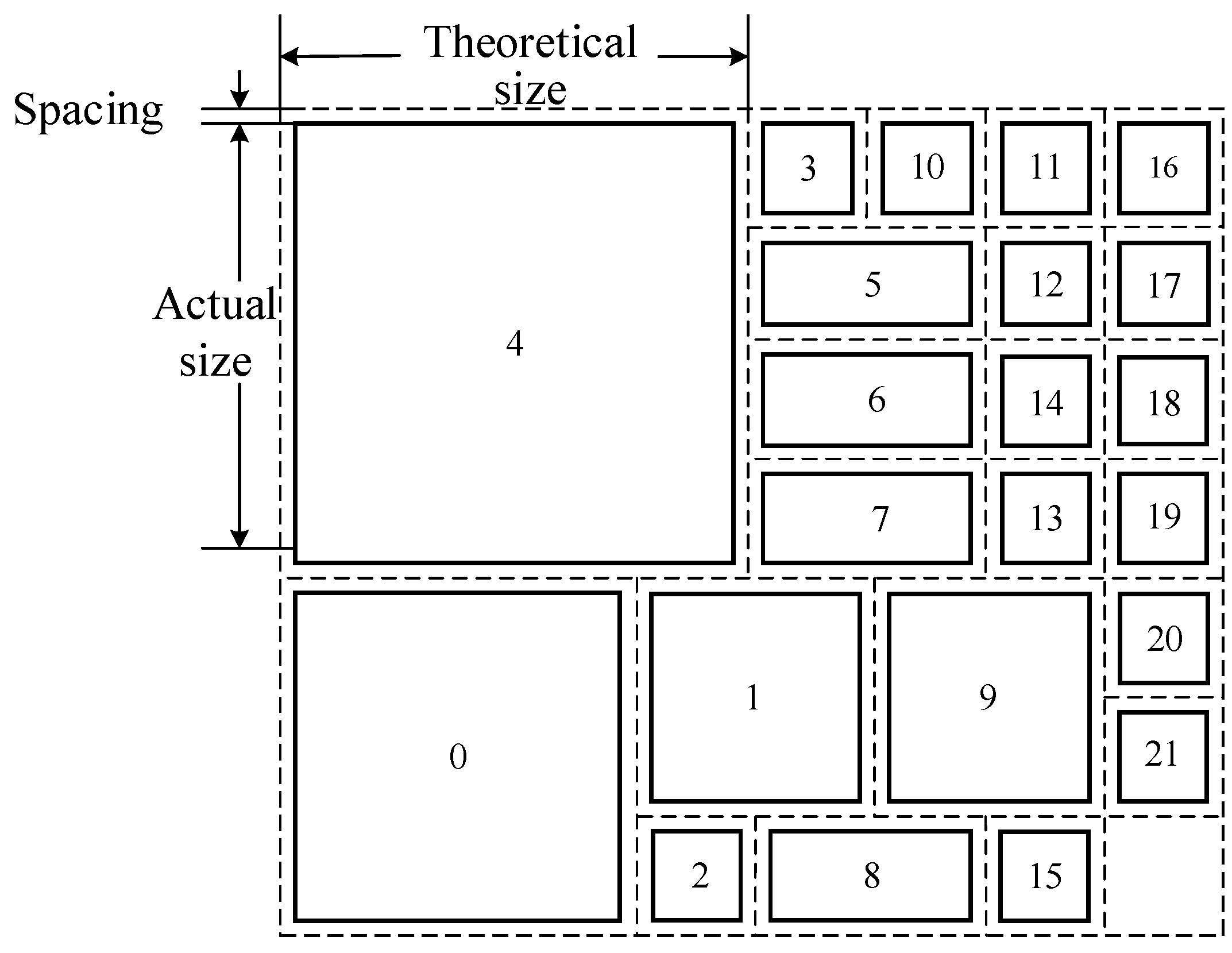
In this algorithm, mesh topology was used. In order to take into account the area factor, it could be assumed that a chiplet mapping with a certain area would occupy multiple nodes in the topology. Meanwhile, there should be a certain spacing between the chiplets, which also needed to be considered. In Figure 1, chiplet numbers are used to represent the chiplets. The chiplet sizes in the algorithm were regarded as the theoretical value based on the actual size containing the spacing, which was slightly larger than the actual size. The theoretical sizes of all chiplets and their numbers are shown in Table 1.

Figure 1.
Schematic diagram of the actual and theoretical dimensions of chiplet 4.

Table 1.
The actual sizes and the theoretical sizes of chiplets.
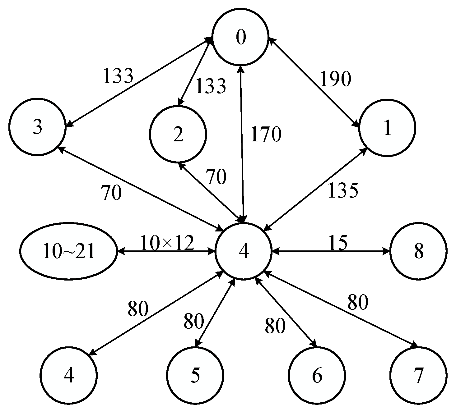
The chiplet communication volume is depicted as a directed graph in Figure 2. Each chiplet (number of chiplets) is represented by a vertex in the graph, and each directed edge represents the communication volume (Mbit/s) between two chiplets.
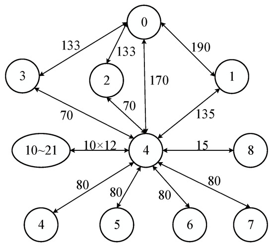
Figure 2.
Communication volume between chiplets of the 2.5-D IC integration.
2.2. Communication Energy Consumption Model
Energy minimization is one of the most important aspects of IC design. In a 2D mesh NoC, the energy consumption of transferring 1 bit of data between node i and j could be described as [17]:
where represents the energy consumption of transferring 1 bit of data from node i to node j. di,j is the Manhattan distance between node i and j. Erouter and ELbit are the energy consumed in routers and links, respectively.
In 2.5-D IC integration, chiplets are directly connected through the interposer. Therefore, the energy consumption can be simplified as:
where is the energy consumption of transferring 1 bit of data from chiplet i to chiplet j. di,j is the Manhattan distance between chiplet i and chiplet j. ELbit is the energy consumed per unit distance.
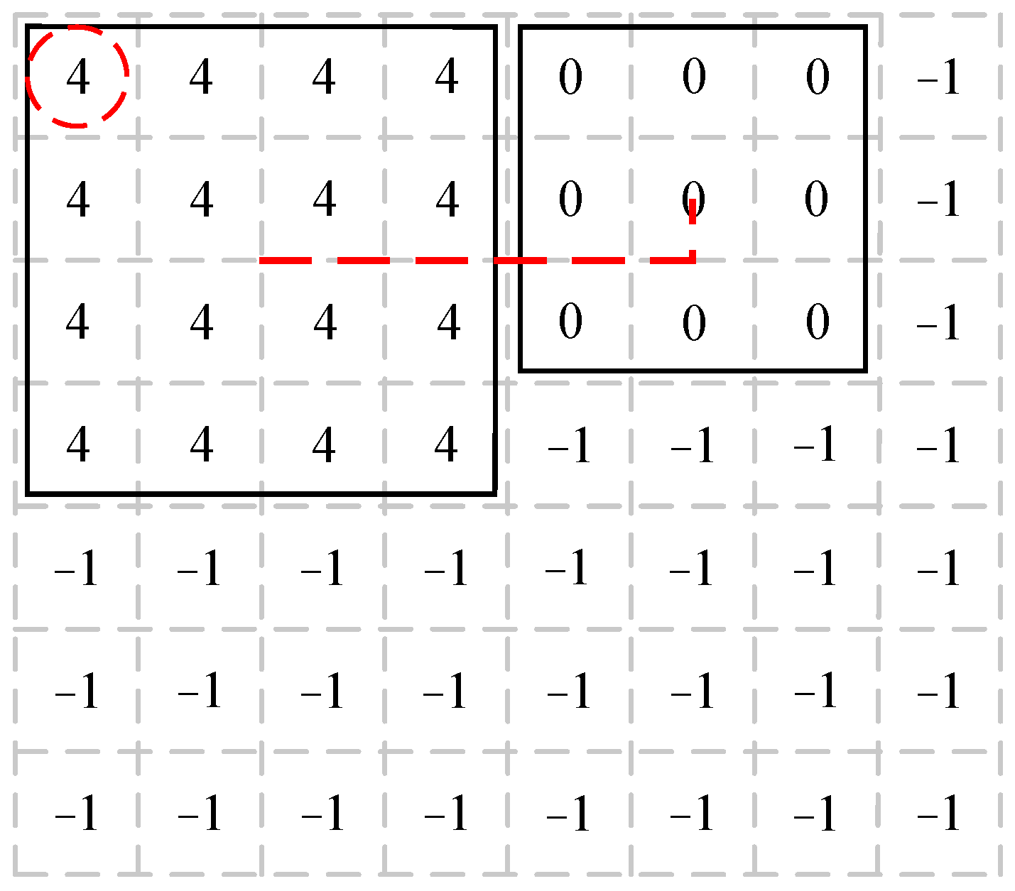
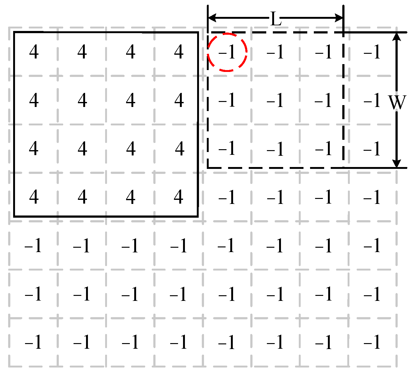
The computing method of distances between chiplets also needed to be examined. In Figure 3, the distances between the chiplet midpoints (dotted line) were used to calculate the average distances. Mapped nodes were given the chiplet number of the corresponding region in the topology, while unmapped nodes were given the initial value “−1”. The node in the top left corner (dashed circle) was used to record the location of the chiplet.
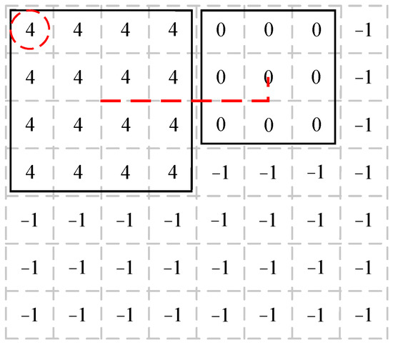
Figure 3.
The representation of chiplet location and distance between chiplets.
The initial layout of the system is shown in Figure 4, and the CEC was 1209.56 μJ, which was calculated by Equation (2).

Figure 4.
The initial layout of the 2.5-D IC integration.
3. Mapping Algorithm Description
This mapping algorithm maps chiplets one after the other by selecting chiplets according to the CPL. Because of the symmetry of the topology, several nodes had the same mapping effect and the number of final schemes was equal to the number of asymmetric initial nodes.
In this algorithm, there were two key phases: Step 1, choose an initial chiplet and map it onto the initial nodes. Step 2, choose the next chiplet and filter the remaining nodes to map it. At the beginning, the function priority_generate generated a CPL. The first chiplet in the CPL, which always has the highest communication volumes with other chiplets, would be mapped first. Following the mapping of the first chiplet, the locations of initial nodes were determined by the function initialnode_generate. The first chiplet in the CPL would be mapped onto the initial nodes. After the first chiplet was mapped, the function next_chiplet selected which chiplet would be mapped next. The location of the next chiplet in the topology was decided by the function next_node for the minimal CEC increment. The CEC increment Eadd could be calculated by Equation (3):
where ELbit is the energy consumed per unit distance. n denotes the number of mapped chiplets. Chiplet j is the chiplet that needs to be mapped, while chiplet i represents the chiplet that has already been mapped. di,j is the distance between chiplet j and chiplet i. If chiplet j communicated with chiplet i, s0 would be “1”. If chiplet i was mapped, s1 would be “1”. Aside from that, s0 and s1 would be “0”.
The next selected chiplets and nodes were checked continually by the function of next_chiplet and next_node, until all chiplets were mapped. In this algorithm, different initial nodes generated different mapping schemes, and the total CEC of each scheme was calculated. The mapping scheme with the minimal CEC would be the algorithm result. Algorithm 1 gives the pseudo-code of our algorithm.
The following sections went over the specifics of the above functions.
| Algorithm 1 The pseudo-code of chiplet communication energy consumption optimal algorithm |
| Input: a chiplet size table. a chiplet communication graph. a topology graph. Output: a mapping result mapbest with best energy consumption. |
| 1. Obtain CPL by priority_generate(G); 2. Initial chiplet i = first chiplet in CPL; 3. Initial node set ITS = initialnode_generate(M); 4. Communication energy consumption CECmin = +∞; 5. For (k = 1; k ≤ |ITS|; k++) { 6. Gmapped = ∅; Gummaped = G; Tunmapped = T; 7. mapk(ci) = tk; Tunmapped = Tunmapped − {tk};//tk ∈ITS 8. Gmapped = Gmapped +{ci}; Gunmapped = Gunmapped − {ci}; 9. While (Gunmapped ≠ ∅) { 10. Next selection chiplet cj = next_priority (Gunmapped,Gmapped); 11. Next selection node tn = next_node (Tunmapped); 12. mapk(cj) = tn; Tunmapped = Tunmapped − {tn}; 13. Gmapped = Gmapped +{cj}; Gunmapped = Gunmapped − {cj};} 14. CECk = calculate_cec (mapk ( )); 15. If (CECk < CECmin) { 16. CECmin = CECk; mapbest = mapk ( );}} 17. Return mapbest ( ); |
3.1. The Priority_Generate Function
The priority_generate function was used to generate the CPL, and the mapping order was based on the CPL. The chiplet that had the largest communication volume with other chiplets would be the first in the CPL. In addition, the chiplet that had the largest communication volume with the already mapped chiplets would be chosen as the next chiplet in the CPL. If chiplets had the same communication volumes with others, the mapping order would be considered to have no differences. Table 2 shows the CPL for this example.

Table 2.
CPL of the 2.5-D IC integration with 22 chiplets.
3.2. The Initialnode_Generate Function
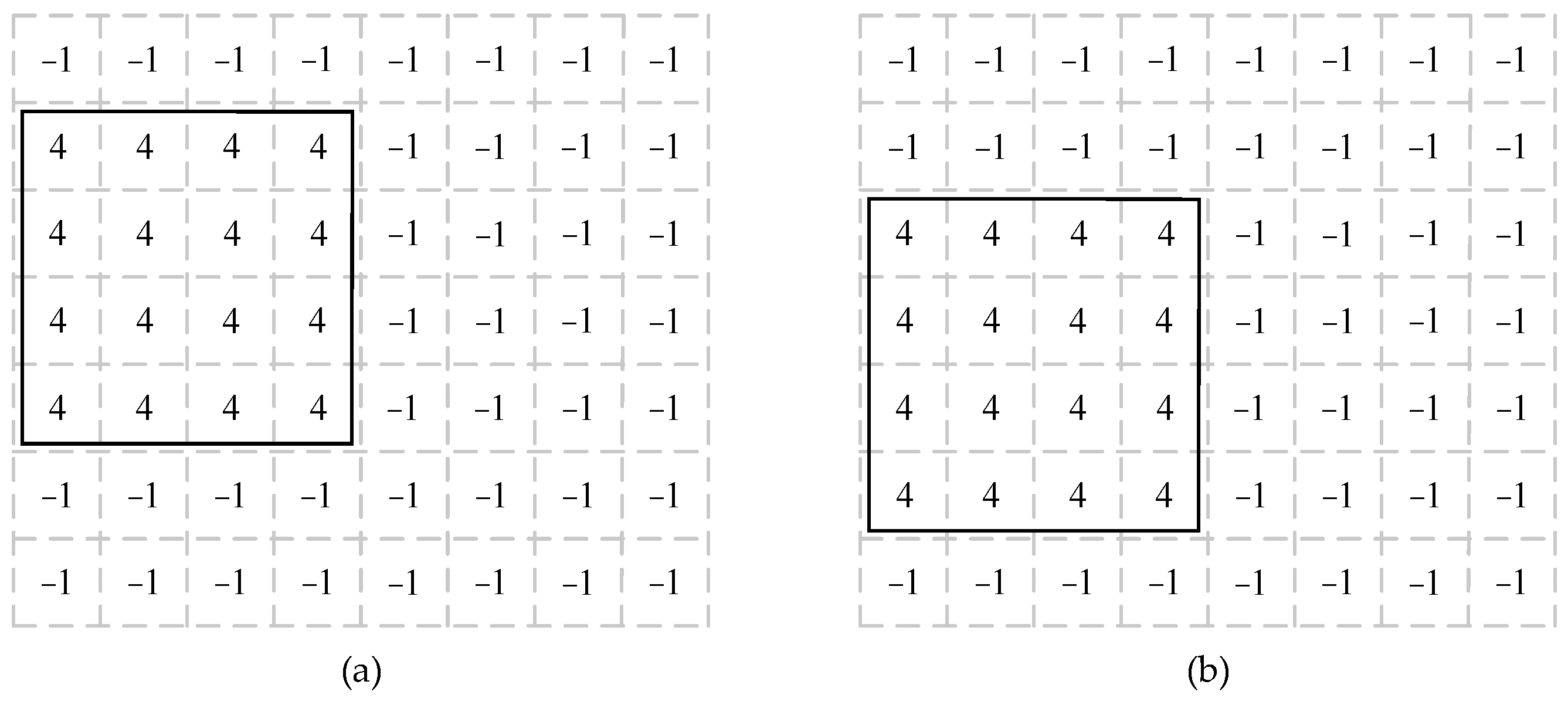
The mapping schemes generated by the CCEOA correspond to initial nodes. Different initial nodes resulted in different layouts. The initialnode_generate function determined these initial nodes. In mesh topology, some nodes had the same mapping effect due to symmetry. Only the CECs of these asymmetric nodes needed to be considered during the algorithm search. Figure 5a shows an example of the initial layout, and Figure 5b shows the symmetrical layout with the same mapping effect.

Figure 5.
(a) An example of initial chiplet placement. (b) Symmetrical placement with the same mapping effect.
The number of initial nodes was also related to the size of the initial chiplet. It could be obtained from Equation (4):
where ceil is the upward rounding function; N1 is the length of the topology; N2 is the width of the topology; L0 is the length of the first mapped chiplet; W0 is the width of the first mapped chiplet; and M is the number of initial nodes.
3.3. The Next_Chiplet Function
The next_chiplet function determines the next chiplet once the initial chiplet is mapped. In this function, chiplets were searched by the Algorithm 2. “N” is the number of the chiplets. The chiplet that was not mapped would be marked “−2” in the chiplet-mapping flag matrix G(k). The communication between chiplets was recorded by the matrix cost(k1) (k2).
| Algorithm 2 The next_chiplet function |
| Input: chiplet priority list, CPL. a chiplet mapping flag matrix, G(k). a chiplet communication matrix, cost(k1) (k2). Output: the next chiplet tk. |
| 1. For (k1 = 0; k1 < N; k1++) { 2. tcost = 0, tmax = 0; 3. If (G[k1] != −2){ 4. For (k2 = 0; k2 < N; k2++){ 5. If (G[k2] == −2 && cost[k1] [k2] > 0) 6. tcost = tcost + cost[k1] [k2];} 7. If (tcost > tmax){ 8. tmax = tcost; 9. tk = k1;}}} 10. Return tk; |
3.4. The Next_Node Function
The location of the next chiplet can be determined by the next_node function. During the mapping process, only unmapped regions larger than the size of the chiplets could map it. For example, the size of the initial chiplet (chiplet 4) was 4 × 4 (L × W), while the second chiplet (chiplet 0) was 3 × 3 (L × W). In Figure 6, if the nodes in a region of length L and width W are all “−1” and do not exceed the topology boundary, the node in the upper left corner of the area (dashed circle) can be used as a mapping node.

Figure 6.
Schematic diagram of the next node screening method.
Usually, there may be multiple nodes making the CEC increment Eadd equal. At this time, the secondary local exploration algorithm can be applied. Algorithm 3 gives the main part of the secondary local exploration algorithm.
| Algorithm 3 Secondary local exploration algorithm |
| Input: the CEC of the chiplet to be mapped, tcost. a chiplet mapping flag matrix, G(k). a chiplet communication matrix, cost(k1) (k2). Output: The next chiplet tk. |
| 1. tmin = 0, tmax = 0, tp = 0; 2. If (tcost < tmin) { 3. tmin = tcost 4. tp = k1;} 5. Else if (tcost = tmin){ 6. For (k1 = 0; k1 < N; k1++) { 7. tcost = 0; 8. If (G[k1] != −2) { 9. For (k2 = 0; k2 < N; k2++) { 10. If (G[k2] == −2 && cost[k1] [k2] > 0) 11. tcost = tcost + cost[k1] [k2]; } 12. If (tcost > tmax || (tcost == tmax && 13. DG[k3] > DG[tk2])) { 14. tmax = tcost; 15. tk2 = k1; 16. tcost = 0;}}} 17. Return tk2; |
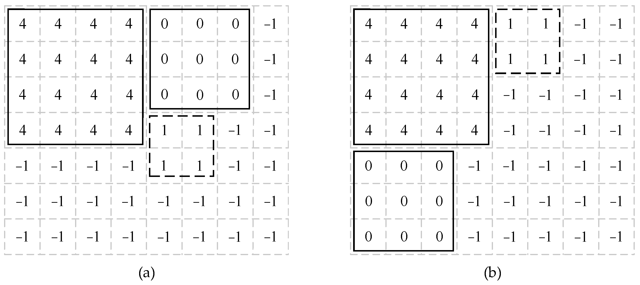
As shown in Figure 7, assuming that the chiplet to be mapped is chiplet 0, the CECs for the cases in Figure 7a,b are the same. At this point, the mapping position of chiplet 0 would be determined by the next chiplet (chiplet 1). In Figure 7a, the unmapped nodes were filtered and mapped for chiplet 1 (dashed box), and the minimum CEC increment was ∆E1. Similarly, in the case shown in Figure 7b, the unmapped nodes were filtered and mapped for chiplet 1 (dashed box) and the minimum CEC increment was ∆E2. If ∆E2 was greater than ∆E1, Figure 7a would be chosen as the mapping scheme for chiplet 0. Conversely, if ∆E1 was greater than ∆E2, Figure 7b would be selected as the mapping scheme for chiplet 0.
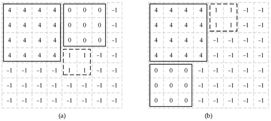
Figure 7.
The method of secondary local exploration. (a) One of the layouts of chiplet 0 with minimum CEC. (b) An alternative layout for chiplet 0 with the same CEC.
Then, the optimal CEC increment Eadd could be expressed by Equation (5):
where is the CEC increment of Figure 7a, and is the CEC increment of Figure 7b.
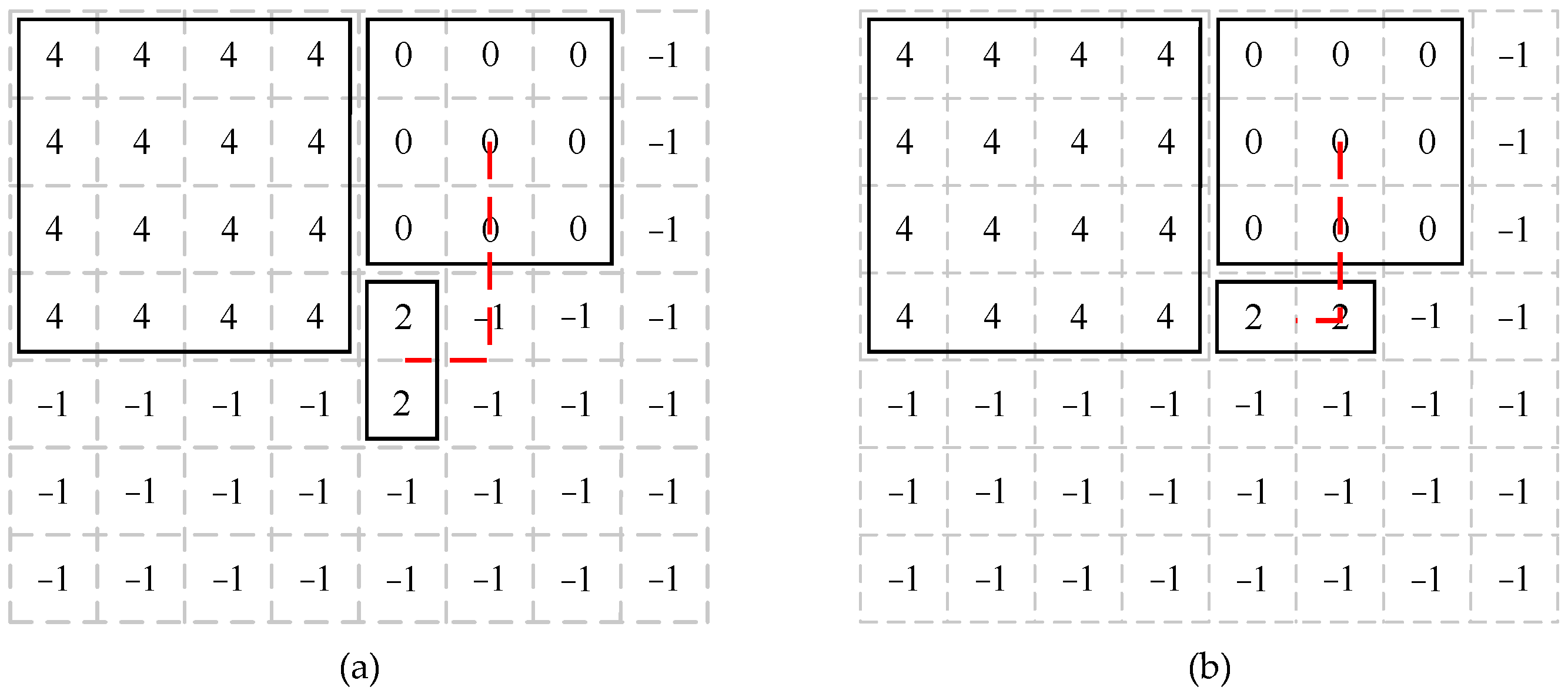
In addition, when considering the distances of the chiplets with different shapes, the distances (dotted line) between the midpoints of chiplets could be taken as the average distances, as shown in Figure 8. When calculating the distances between chiplets in this way, the distances between chiplets placed horizontally and vertically would also be different. In Figure 8, the dotted line is the Manhattan distance between the chiplets. When the chiplets were placed vertically, the distance between chiplet 0 and chiplet 2 was 3.5 units, while when the chiplets were placed horizontally, the distance between the two chiplets was 2.5 units. Therefore, the horizontal and vertical placements should have been calculated separately, and we could obtain the minimum Eadd by the following Equation (6):
where Eaddhor is the CEC increment of the chiplet placed horizontally and Eaddver is the CEC increment of the chiplet placed vertically.
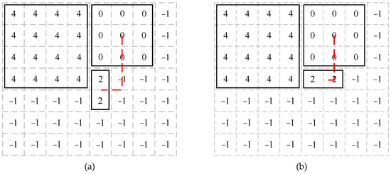
Figure 8.
The distance between chiplets placed (a) vertically and (b) horizontally.
According to these steps, the next_node function would decide which node was selected.
4. Experiment Results
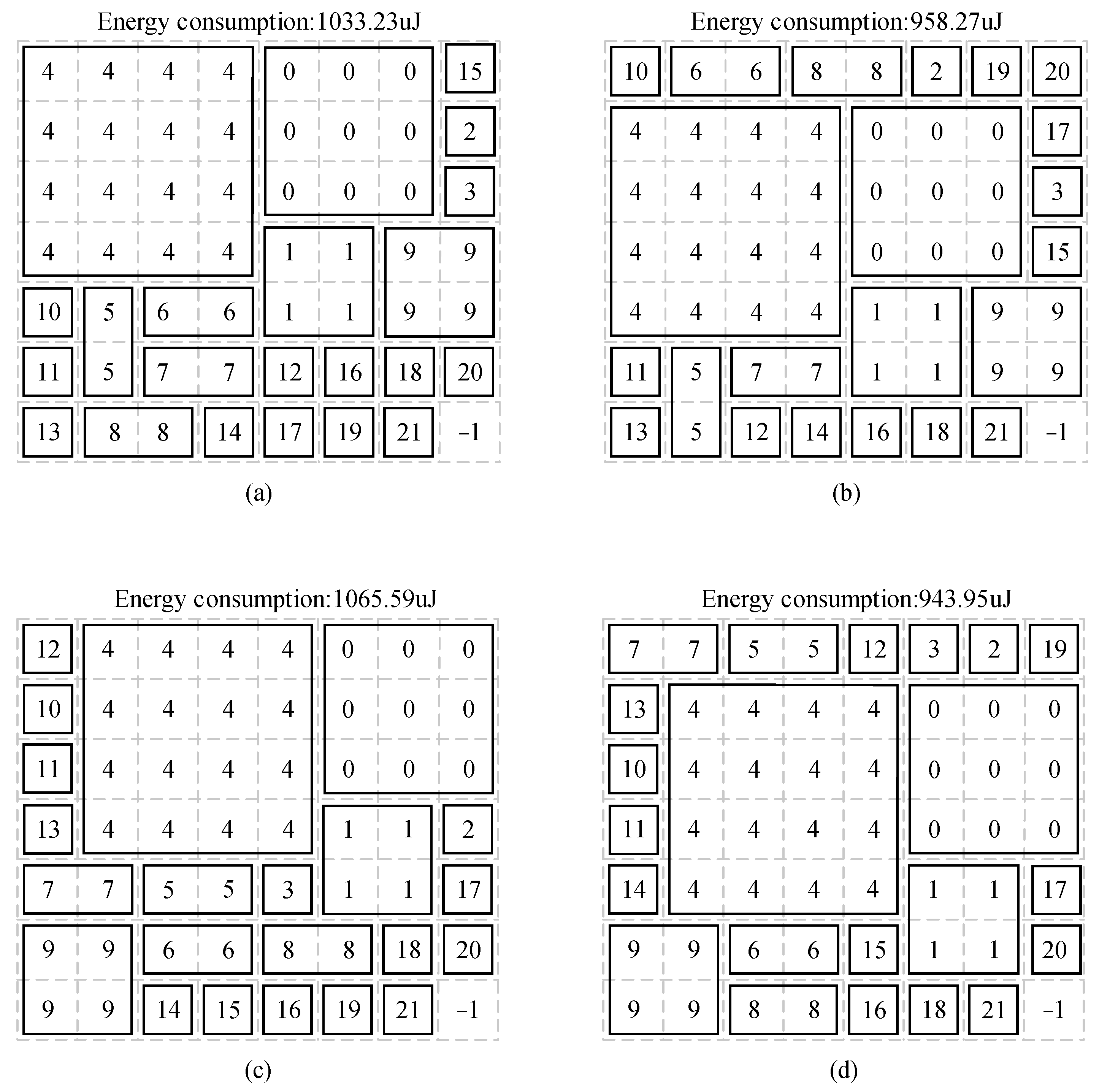
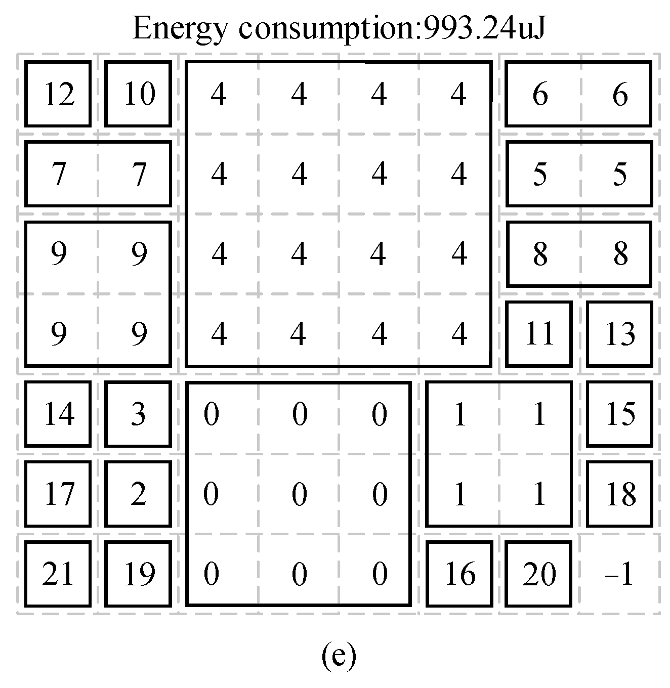
This study used the C++ language to implement the CCEOA in order to verify its performance and efficiency. To examine the mapping process and algorithm performance, we used a 2.5-D IC integration with 22 chiplets as an example. The entire algorithm took only 0.101 s to produce all the results. The layout of the chiplets could be derived very efficiently. According to initialnode_generate function, the initial nodes had five different distributions, and the algorithm could obtain five alternative final mapping schemes, as illustrated in Figure 9. In Figure 9d, the optimal CEC was 943.95 μJ. The chiplet with the highest communication volume was in the middle, and the other chips with which it communicated were distributed around it, minimizing the distance and CEC between them.

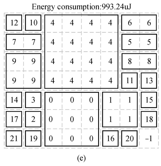
Figure 9.
Results of the algorithm corresponding to different initial nodes. Energy consumption: (a) 1033.23 μJ; (b) 958.27 μJ; (c) 1065.59 μJ; (d) 943.95 μJ; (e) 993.24 μJ.
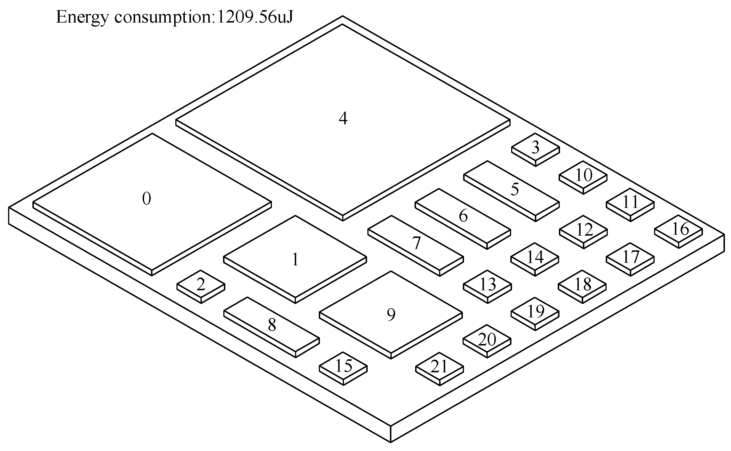
In Figure 10a, compared with the original layout placement, all CECs of these schemes obtained by our algorithm were lower than the initial layout. The CEC of the optimal scheme was 943.95 μJ (Figure 10a), which was 22.0% lower than the initial layout. Figure 10b shows the 3D schematic diagram of the optimal result.
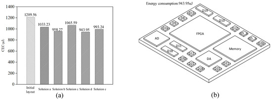
Figure 10.
(a) Contrast of initial layout and CCEOA results; (b) 3D schematic diagram of the optimal result.
5. Conclusions
A proper layout of chiplets in 2.5-D integration could improve the communication energy consumption of the whole system. In this paper, we proposed an algorithm considering the area factor of the chiplet using multiple nodes to map them based on the SYMMAP algorithm. At the same time, due to the area factor, we examined the selection of unmapped nodes, including secondary local exploration methods. The CECs of the horizontal placement and vertical placement were also calculated, respectively, and the smaller value was taken as the result. Through the above steps, we could complete the mapping of chiplets and obtain a chiplet layout placement with a low CEC. Based on a 2.5-D IC integration with 22 chiplets, the CEC of the optimal scheme of our algorithm was 22% lower than the initial layout. Furthermore, based on our heuristic algorithm, the inputs, including the numbers and sizes of chiplets and the size of the topology, could be modified to suit the needs of different systems.
Author Contributions
Conceptualization, H.S. and Y.L.; methodology, H.S. and X.P.; software, H.S., X.P. and D.C.; validation, X.P.; formal analysis, X.P.; investigation, X.P. and D.C.; data curation, D.C.; writing—original draft preparation, X.P. and D.C.; writing—review and editing, H.S. and X.P.; visualization, D.C.; supervision, H.S. and J.Z. All authors have read and agreed to the published version of the manuscript.
Funding
This research was funded by the National Natural Science Foundation of China (Grant No. 61974077).
Conflicts of Interest
The authors declare no conflict of interest.
References
- Moore, G.E. Cramming More Components Onto Integrated Circuits. Proc. IEEE 2002, 86, 82–85. [Google Scholar] [CrossRef]
- Kabir, M.A.; Peng, Y. Holistic Chiplet–Package Co-Optimization for Agile Custom 2.5-D Design. IEEE Trans. Compon. Packag. Manuf. Technol. 2021, 11, 715–726. [Google Scholar] [CrossRef]
- Lim, S.P.S.; Chidambaram, V.; Jaafar, N.; Seit, W. Development of 2.5 D high density device on large ultra-thin active interposer. In Proceedings of the 2019 IEEE 21st Electronics Packaging Technology Conference (EPTC), Singapore, 4–6 December 2019. [Google Scholar]
- Chaware, R.; Nagarajan, K.; Ramalingam, S. Assembly and reliability challenges in 3D integration of 28nm FPGA die on a large high density 65nm passive interposer. In Proceedings of the Electronic Components & Technology Conference, San Diego, CA, USA, 29 May–1 June 2012. [Google Scholar]
- Coskun, A.; Eris, F.; Joshi, A.; Kahng, A.B.; Ma, Y.; Narayan, A.; Srinivas, V. Cross-layer co-optimization of network design and chiplet placement in 2.5-D systems. IEEE Trans. Comput.-Aided Des. Integr. Circuits Syst. 2020, 39, 5183–5196. [Google Scholar] [CrossRef]
- Kim, J.; Murali, G.; Park, H.; Qin, E.; Kwon, H.; Chekuri, V.C.K.; Rahman, N.M.; Dasari, N.; Singh, A.; Lee, M.; et al. Architecture, Chip, and Package Codesign Flow for Interposer-Based 2.5-D Chiplet Integration Enabling Heterogeneous IP Reuse. IEEE Trans. Very Large Scale Integr. (VLSI) Syst. 2020, 28, 2424–2437. [Google Scholar] [CrossRef]
- Kim, J.; Chekuri, V.C.K.; Rahman, N.M.; Dolatsara, M.A.; Torun, H.; Swaminathan, M.; Mukhopadhyay, S.; Lim, S.K. Silicon vs. Organic Interposer: PPA and Reliability Tradeoffs in Heterogeneous 2.5 D Chiplet Integration. In Proceedings of the 2020 IEEE 38th International Conference on Computer Design (ICCD), Hartford, CT, USA, 18–21 October 2020. [Google Scholar]
- Li, T.; Hou, J.; Yan, J.; Liu, R.; Yang, H.; Sun, Z. Chiplet heterogeneous integration technology—Status and challenges. Electronics 2020, 9, 670. [Google Scholar] [CrossRef] [Green Version]
- Lau, J.H. Recent advances and trends in advanced packaging. IEEE Trans. Compon. Packag. Manuf. Technol. 2022, 12, 228–252. [Google Scholar] [CrossRef]
- Kim, J.; Chekuri, V.C.K.; Rahman, N.M.; Dolatsara, M.A.; Torun, H.M.; Swaminathan, M.; Mukhopadhyay, S.; Lim, S.K. Chiplet/Interposer Co-Design for Power Delivery Network Optimization in Heterogeneous 2.5-D ICs. IEEE Trans. Compon. Packag. Manuf. Technol. 2021, 11, 2148–2157. [Google Scholar] [CrossRef]
- Kabir, M.A.; Peng, Y. Chiplet-package co-design for 2.5 D systems using standard ASIC CAD tools. In Proceedings of the 2020 25th Asia and South Pacific Design Automation Conference (ASP-DAC), Beijing, China, 13–16 January 2020. [Google Scholar]
- Park, H.; Kim, J.; Chekuri, V.C.K.; Dolatsara, M.A.; Nabeel, M.; Bojesomo, A.; Patnaik, S.; Sinanoglu, O.; Swaminathan, M.; Mukhopadhyay, S.; et al. Design Flow for Active Interposer-Based 2.5-D ICs and Study of RISC-V Architecture With Secure NoC. IEEE Trans. Compon. Packag. Manuf. Technol. 2020, 10, 2047–2060. [Google Scholar] [CrossRef]
- Murali, S.; De Micheli, G. Bandwidth-constrained mapping of cores onto NoC architectures. In Proceedings of the Design, Automation and Test in Europe Conference and Exhibition, Paris, France, 16–20 February 2004. [Google Scholar]
- Wang, X.; Choi, T.M.; Yue, X.; Zhang, M.; Du, W. An effective optimization algorithm for application mapping in network-on-chip designs. IEEE Trans. Ind. Electron. 2019, 67, 5798–5809. [Google Scholar] [CrossRef]
- Liu, Y.; Ruan, Y.; Lai, Z.; Jing, W. Energy and thermal aware mapping for mesh-based NoC architectures using multi-objective ant colony algorithm. In Proceedings of the 2011 3rd International Conference on Computer Research and Development, Shanghai, China, 11–13 March 2011. [Google Scholar]
- Liu, Y.; Ruan, Y.; Lai, Z. New heuristic algorithms for low-energy mapping and routing in 3D NoC. Int. J. Comput. Appl. Technol. 2013, 47, 1–13. [Google Scholar] [CrossRef]
- Ye, T.T.; Micheli, G.D.; Benini, L. Analysis of power consumption on switch fabrics in network routers. In Proceedings of the 39th Annual Design Automation Conference, New Orleans, LO, USA, 10–14 June 2002. [Google Scholar]
Publisher’s Note: MDPI stays neutral with regard to jurisdictional claims in published maps and institutional affiliations. |
© 2022 by the authors. Licensee MDPI, Basel, Switzerland. This article is an open access article distributed under the terms and conditions of the Creative Commons Attribution (CC BY) license (https://creativecommons.org/licenses/by/4.0/).

