1. Introduction
GaN-HEMT has attracted a lot of interest because of its high two-dimensional electron-gas (2DEG) density and electron mobility, which have wide applications in 5G communication, electric vehicles and consumer electronics [
1,
2,
3]. At present, GaN substrates with large sizes and low prices are unavailable, hence GaN materials are mostly epitaxially produced on heterogeneous substrates such as Si, sapphire and silicon carbide. However, due to a large number of defects in heteroepitaxial GaN materials, the BV of GaN-HEMT devices is far from satisfactory, limiting their use in high-power applications. There are several methods to enhance BV [
4,
5]. In the field of epitaxial material growth, using the AlGaN channel to replace the GaN channel [
6,
7] and using the AlGaN as a back-barrier layer [
8] have attracted the attention of researchers. The AlGaN back-barrier layer can lift the conduction band on the side of the channel and reduce electron leakage to the buffer layer [
9], and the theoretical breakdown voltage of AlGaN is also higher than that of GaN. However, the introduction of the AlGaN back-barrier will weaken the polarization effect in the heterojunction, and the higher the Al component is, the more the polarization effect will be weakened, resulting in a considerable reduction in the I
D of the device [
10,
11,
12,
13]. Zhang et al. [
14] introduced the p-type region in the GaN buffer layer, which improved the breakdown voltage of the device by making the distribution of the electric field more uniform. Jun et al. [
15] used a double p-type-doped layer in the buffer layer in a HEMT with an 8 μm gate-drain distance, and the BV was enhanced due to the decreased peak electric field. However, the preceding studies examined only the GaN buffer layer and ignored the effect of introducing a local p-doped region on the I
D.
It is necessary to enhance the BV of the device as much as feasible under the condition of high I
D to accomplish the use of the HEMT device in high-power applications. In this study, we used a local p-doped region in the traditional AlGaN back-barrier structure to reduce the peak electric field and increase the BV, while also investigating its effect on I
D. Even though the local p-doping in AlGaN material is still being developed, it is critical to provide a direction for balancing the I
D and BV of back-barrier application. In this study, the I-V characteristics, the BV characteristics, the distribution of the electric field in the device and the distribution of the space charge in the buffer layer were obtained by a SILVACO ATLAS simulator. We had already used the reference data [
7] to calibrate the simulation results to the experimental data before we carried out this simulation.
2. Structures and Simulation
The two structures used in the simulation are shown in
Figure 1. The schematic in
Figure 1a is the conventional back-barrier structure.
Figure 1b depicts the proposed structure for introducing the local p-doped region in the back-barrier. Both of them are based on an Al
0.45Ga
0.55N/Al
0.15Ga
0.85N heterojunction. The gate width and length are 100 μm and 1.5 μm, respectively. The gate–source distance is 2.5 μm, and the gate–drain distance is 5 μm. The width of the cross section of each structure is set to 10 μm, and the thickness of the barrier layer and channel layer is 25 nm and 50 nm, respectively. D1, D2 and D3 in
Figure 1b are the distance from the doped region to the channel, the width of the doped region and the distance between the region and the drain, respectively.
The Al component of the buffer layer in both structures was fixed at 0.18 at first. For the proposed structure, the uniform doping concentrations of 3 × 10
16 cm
−3, 5 × 10
16 cm
−3 and 7 × 10
16 cm
−3 were employed in the Al
0.18GaN back-barrier separately. The D1, D2 and D3 were set at 200 nm, 4.5 μm and 2 μm to obtain the effects of different doping concentrations on BV and I
D. It should be noted that the initial X coordinate of D3 was set to 3.5–8 μm, and it was adjusted when we studied the influence of the position of the doped region on the BV. The passivation layer was silicon nitride, and its thickness was 300 nm. For the buffer layer, a 1 × 10
15 cm
−3 concentration was taken as the background-carrier density. The acceptor-like trap’s density of 1 × 10
17 cm
−3 was also considered in the buffer layer for both structures [
16]. The Newton iteration was used in the simulation.
In this work, the polarization model was used for imitating the spontaneous and the piezoelectric polarization effect. The polar scale was set as 0.6, and the polarization charge in the heterojunction is 1.029 × 10
20 cm
−3 at this setting. A Shockley–Read–Hall model and Fermi–Dirac statistics were utilized in the simulation. In addition, the Albrecht model was chosen as the low-field mobility model, and a high-field mobility model based on Monte Carlo data for bulk nitride was also used [
17]. For the BV characteristics, the Selberherr impact ionization model was taken and the coefficients in that model were adjusted following the work of Hideyuki et al. [
16] and Bulutay [
18]. The work function of the gate electrode was set to 5.0 eV and 4.04 eV for the source and the drain, respectively, and the contact length was set as 0.5 μm. For a fair comparison, the physical parameters and models mentioned above were used for both structures. The drain voltage was chosen as the off-state BV when I
D reached 1 mA/mm at V
gate = −10 V. The lat.temp model was considered when we investigated the device’s BV in different temperatures.
3. Results and Discussion
The BV characteristics of the two structures are shown in
Figure 2. In
Figure 2a, the BV corresponding to the Al
0.18Ga
0.82N back-barrier structure is 1068.44 V. In the device with three local p-doped regions, the BV was found to be 1107.14 V, 1139.67 V and 1179.21 V, respectively, for the doping concentrations of 3 × 10
16 cm
−3, 5 × 10
16 cm
−3 and 7 × 10
16 cm
−3, which means that the BV of the device increases when the doping concentration increases.
The breakdown of the device normally happens at the peak electric field. Thus, the BV of the device is higher when the internal peak electric field is weakened. We considered the distribution of electric field below the heterojunction in the structure at V
ds = 650 V and V
gate = −10 V, which is shown in
Figure 2b. The peak electric field in the device at three doping concentrations was lower than the Al
0.18Ga
0.82N back-barrier structure, and the higher the doping concentration was, the smaller the peak electric field was. When the doping concentration was 7 × 10
16 cm
−3, the peak electric field decreased by 3.06 × 10
5 V/cm, and the BV increased to 1179.21 V correspondingly, with an increase of about 11%. That means that the p-type doped region can weaken the electric field because there is a space charge region in the back-barrier layer due to the reversed PN junction, which is formed by a hole in the p-doped region and the electron in the back-barrier layer [
15,
19]. The positive electron in a doped region can attract part of the electric field, resulting in a rise in another peak in the electric field distribution. As the doping concentration increases, the space charge region becomes larger, which is shown in
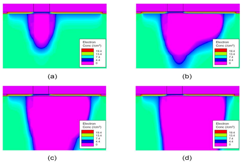
Figure 3, and the presence of the space charge region can also weaken the transverse electric field [
14]. Furthermore, the electron mobility in the space charge region is limited, which reduces the probability of collision ionization and increases the BV.
For the output characteristics of the two structures, as shown in
Figure 4a, we increased the Al component of the back-barrier in
Figure 1a from 0.18 to 0.20 and 0.22. When V
gate = 0 V, the maximum output current density (I
Dmax) reduced from 783.9 mA/mm to 704.3 mA/mm and 596.9 mA/mm, which decreased by about 10% and 24%, respectively, while the BV increased by only about 5% and 14%. The reason for the drop in I
D is that the buffer layer is thick in general, which could be considered a completely relaxed state. The channel layer on the top of it is thin, and it is under compressive strain, weakening the lattice mismatch in the heterojunction and decreasing the polarization effect. For the structure with the local p-doped region, the I
Dmax decreased by only 23.3/49.4/66.1 mA/mm at three concentrations, although p-type doping can deplete the 2DEG in the channel [
20]. The preceding results show that the introduction of a local p-doped region can not only improve the BV of the device, but also reduce the influence on the I
D. The transfer characteristics of the structures are shown in
Figure 4b, and the introduction of the local p-doped region does not affect the threshold voltage of the device. The electron concentration and conduction band (E
C) near the heterojunction are shown in the inset of
Figure 4b, which is consistent with the change in the I
D.
The transconductance (g
m) of the two structures is compared in
Figure 5. We found that the g
m was slightly increased in the structure with the p-doped region, and this is because the electron mobility increased as the 2DEG density decreased. The f
T of the traditional Al
0.18GaN back-barrier structure and the proposed structure with 7 × 10
16 cm
−3 was found to be 1.19 GHz and 1.23 GHz, respectively. Because the heterojunction in the study is made entirely of AlGaN, the alloy-disordered scattering will rise, and the RF characteristics will be inferior to those of devices with an AlGaN/GaN heterojunction.
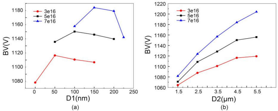
We also investigated the effect of the distance (D1) between the top of the doped region and the channel on the BV with three different doping concentrations.
Figure 6a shows that there were different optimized values of D1 for different doping concentrations: when D1 was 50 nm, which indicates that the doped region is 100 nm away from the heterojunction, the structure with the 3 × 10
16 cm
−3 doping concentration had the largest BV of 1116.44 V. The optimized values of D1 are 100 nm and 150 nm for doping concentrations of 5 × 10
16 cm
−3 and 7 × 10
16 cm
−3, respectively. The corresponding BVs were found to be 1150.22 V and 1184.07 V, respectively. It may be noted that the optimal value of D1 varies with different doping concentrations. The reason for this is that when D1 is bigger, a larger p-type doping concentration is required to generate a larger space charge area, allowing for a stronger modulation on the electric field [
14].
In addition, as shown in
Figure 6b, we compared the BV with different doping lengths (D2). When D1 was fixed as an optimized length for each concentration and the left boundary of the doping region was fixed, D2 varied from 1.5 μm to 5.5 μm. The BV increased with D2 for each doping concentration without exception. The reason for this is that when D2 became larger, a larger depletion region occurred. For 7 × 10
16 cm
−3, the BV increased from 1081.64 V to 1204.18 V when D2 varied from 1.5 μm to 5.5 μm.
Figure 7 shows the effects of changes in D1 and D2 on I
D. The I
D increased quietly with the D1. However, when D1 was fixed, the effect of the change in D2 on I
D could be ignored. That is, the depletion of the 2DEG by the p-doped region is mostly dependent on distance rather than length. However, the change in I
D is slight, so the geometric parameter of the p-doped region could be adjusted for a higher BV.
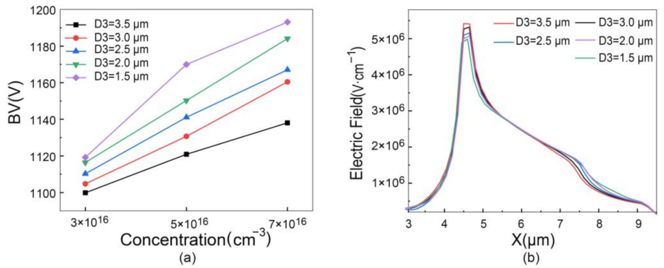
Furthermore, when D1 was set to the optimal value for those concentrations, the BV was higher when the doped region was closer to the drain, as shown in
Figure 8a. The electric field distribution is plotted in
Figure 8b, illustrating the electric field distribution when the concentration was 7 × 10
16 cm
−3 and D1 = 150 nm. It was observed that when the doped region was closer to the drain, the electric field weakened more obviously, which is consistent with the improvement in the BV. When the distance between the doped region and the drain was changed from 3.5 μm to 1.5 μm, the X coordinate of the corresponding doped region ranged from 2–6.5 μm to 4–8.5 μm. The peak electric field below the heterojunction decreased from 5.42 × 10
6 V/cm to 4.98 × 10
6 V/cm, and the BV increased from 1138.06 V to 1193.09 V.
Finally, we took the lattice heating into consideration, and obtained the BV of the traditional structure and the structure with 7 × 10
16 cm
−3 doping under different temperatures where the simulation parameters remained as the initial setting, as shown in
Figure 9. The thermal contact was set at the bottom of the two structures, and the temperature was changed from 300 K to 450 K. When the lattice heating model is considered, the results demonstrate that the BV in the proposed structure is lower than the traditional structure, because the doping in the buffer layer increases the collision–ionization probability at high temperatures.


