1. Introduction
The micro light emitting diode (Micro-LED) refers to a high-density, integrated LED array [
1]. A micro-LED display uses inorganic LED devices as light-emitting pixels to realize an active light-emitting matrix display, which surpasses the current mainstream liquid crystal (LCD) and organic light-emitting diode (OLED) displays, in terms of power consumption, resolution, contrast and life, and represents significant progress in the area of display fields [
2,
3,
4]. The performance parameters of related devices are shown in
Table 1. The size of a micro-LED is reduced to the micron level (generally less than 50 μm) [
5], which can realize the control of each pixel and a single-point light drive, and the single pixel produces high brightness [
6]. The application prospects are very broad, and they are widely used in virtual reality displays, neuron stimulation, optical wireless communication and other fields [
7,
8,
9]. However, the application of micro-LED still faces some challenges, such as: small size effect; chip and backplane technology; mass transfer technology; full-color technology; bonding and driving technology; defect and yield technology; inspection and maintenance technology; etc. [
10,
11,
12,
13,
14]. Driving technology is also one of these challenges [
15].
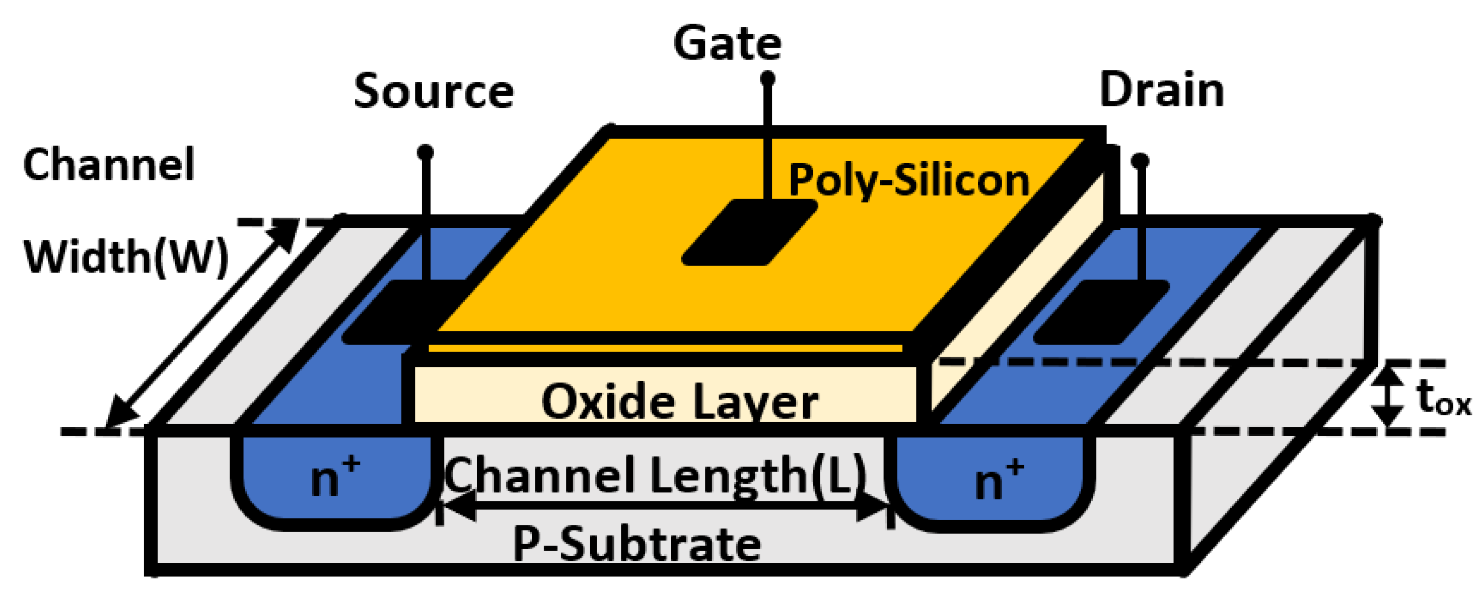
A metal-oxide-semiconductor field effect transistor (MOSFET) is the basic unit of MOS and digital CMOS integrated circuits. It is a field effect transistor that can be widely used in analog circuits and digital circuits. The basic structure of an N-channel polysilicon gate MOS transistor is shown in
Figure 1.
A complementary metal oxide semiconductor (CMOS) inverter represents the basic module of a CMOS digital integrated circuit based on a CMOS inverter [
16]. The size of CMOS devices can be easily reduced—analog and digital circuits can be placed on the same chip—and the manufacturing cost of CMOS circuits is low [
17]. Under the condition of the same geometric size and absolute value of working voltage, the NMOS transistor has a large transconductance and small on resistance, but the NMOS transistor also has many disadvantages, such as a large volume, complex circuit structures and high costs [
18]. The PMOS transistor has a high threshold voltage and strong anti-interference abilities, but its on-resistance is relatively large, load current is large, and heating is significant [
19]. In 2011, the Shin team conducted research on an NMOS direct driving Micro-LED. They used gold bump bonding and anisotropic conductive adhesive to flip-chip connect an NMOS silicon driving circuit and micro-LED array. The micro-LED array had 8 × 8 pixels and each pixel size was 30 μm × 30 μm [
20]. In the same year, McGovern’s team conducted research on PMOS direct driving micro-LEDs. They used a PMOS driver with a pixel size of 150 μm × 150 μm and a resolution of 64 × 64 to drive gan-based micro-LEDs with a diameter of 25 μm [
21]. However, up to now, there is no research on directly driving a micro-LED with a CMOS inverter [
22,
23,
24,
25,
26].
Therefore, the circuit design of Micro-LEDs driven by CMOS inverters is proposed for the first time in this paper. By designing the structures of NMOS and PMOS devices and defining related parameters, and comparing the three driving modes of NMOS, PMOS and CMOS inverters to drive individual Micro-LEDs by TCAD simulation, the best driving circuit was determined according to the current characteristics of the transient characteristic curve of the simulation results, which lays a foundation for the design of an array micro-LED driving circuit.
2. Simulation Parameters and Model Settings
In this paper, based on the SWB environment of Sentaurus software, the design and application of the TCAD simulation project is organized and implemented, and the TCAD project is realized in parametric form. Through simulation and analysis of the characteristics of the 0.18 μm process MOS transistor, the NMOS transistor and PMOS transistor which meet the requirements of this experiment, were designed, and the CMOS inverter was designed and built. The circuit of the CMOS inverter driving the micro-LED directly is proposed for the first time. By comparing the simulation performance of the NMOS, PMOS and CMOS inverters driving the Micro-LED, the best driving circuit was determined, which laid the foundation for driving an array Micro-LED.
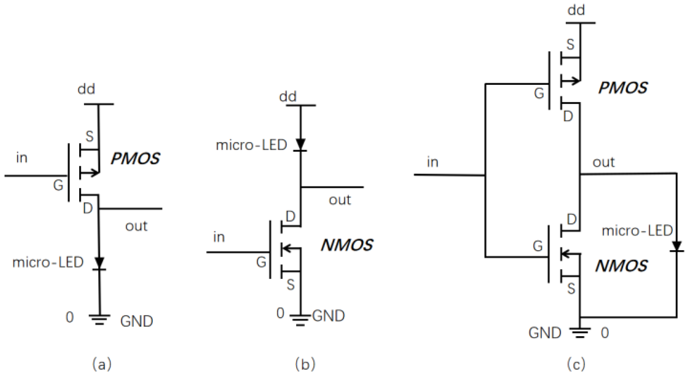
Circuit symbols of an N-channel and P-channel enhancement MOSFET are shown in
Figure 2. In this experiment, nMOSFETs are used as the lower tubes and pMOSFETs as the upper tubes; as shown in
Figure 2a,b.
The variation trend of the width-length ratio of PMOS and NMOS under different process conditions are shown in
Figure 3, and also the width-length ratio W/L = 2.25 under 0.18 μm process conditions. The gate length L is 0.18 μm, which makes the NMOS device width W
N = 2.0 μm and PMOS device width W
P = 4.5 μm. The thickness (tox) of the oxide layer was selected to be 16 Å.
The gate-source voltage V
GS used to generate the surface inversion layer (to generate the conduction channel) is called the threshold voltage
VT0. The threshold voltage formula is:
where
VT0 is the threshold voltage at zero substrate bias;
γ is the substrate bias coefficient;
VSB is the substrate bias voltage;
ϕF is the Fermi potential of the substrate.
Fermi potential formula of n-type semiconductor substrate:
In which k is the Boltzmann constant; q is the unit (electron) charge; T is the temperature (T = 300 K at room temperature); ni is a function of temperature T (ni = 1.45 × 1010 cm−3 at room temperature); NA is the substrate doping concentration.
The work function difference formula between the gate and the channel is:
Charge density formula of the depletion region:
where
εsi is the dielectric constant of silicon;
VSB is the substrate voltage.
The charge formula of oxidation interface is:
where
NOX is the interface of the oxide layer, there is charge density, and
NOX = 2 × 10
10 cm
−2.
The gate oxidation capacitance
COX per unit area can be obtained by the dielectric constant ε
OX and the oxidation thickness
tOX of the silicon oxide layer, and the formula is:
According to the experience of MOSFETs design, a voltage of 0.18 μm process MOSFETs is about 0.5 V, and under the same process conditions, the substrate doping concentration of pMOSFETs is larger than that of nMOSFETs, so the absolute value of the threshold voltage of pMOSFETs is larger than that of nMOSFETs. Therefore, the threshold voltage of the NMOS transistor and PMOS transistor used in this paper is about 0.45 V and −0.5 V respectively. The oxide thickness
tOX of the MOSFETs is set to 16 Å, and the substrate bias is the same as the source potential, that is, V
SB = 0. Combined with formula (1–8), the threshold voltage formula of NMOS transistor can be obtained as follows:
Introducing VTN = 0.45 V into formula (9) can determine the substrate doping concentration (NA) of nMOSFETs to be 3.556 × 1018 cm−3, and similarly, introducing VTP = −0.5 V into the corresponding formula can detemine the substrate doping concentration ND of pMOSFETs to be 4.202 × 1018 cm−3.
The above simulation parameter values were entered into the Sentaurus TCAD simulation software, NMOS and PMOS simulation models were built, and the obtained NMOS simulation device and PMOS simulation device were combined in MixedMode, so that the CMOS inverter simulation device designed by us can be obtained.
Figure 4 shows the structural diagram of the CMOS inverter, in which PMOS is the upper tube, NMOS is the lower tube, and there is a common gate input and common drain output. The PMOS source was connected with a 5 V source voltage, and the NMOS source was grounded. The transmission characteristic curve and transient characteristic curve are important reference curves for testing the electrical performance of the CMOS inverter.
3. The MOS Driving Circuit Drives the Micro-LED
The simulation parameter values were entered into the Sentaurus TCAD simulation software to simulate the electrical characteristics of the MOSFETs, and the parameters were adjusted according to the obtained output characteristic curve, so as to obtain various physical parameters of MOSFETs, and the simulation value of the threshold voltage of MOSFETs was obtained according to the transfer characteristic curve, which is compared with the expected threshold voltage value, so as to judge whether the simulation result is correct or not.
The simulation result of NMOS and PMOS structure models are shown in
Figure 5.
Figure 5a,b are the physical structure model simulation diagrams of NMOS and PMOS devices, respectively. The length of the model simulation diagram is 1.48 μm and the height is 1.2 μm.
Figure 5c is a simulation graph of transmission characteristics of NMOS devices. When the gate voltages are fixed at 1.0 V, 2.0 V, 3.0 V, 4.0 V and 5.0 V, respectively, the relationship curves between drain current and drain voltage are obtained. It can be found that when the gate voltage is greater than the turn-on voltage, the drain current curve shows a linear curve when the drain voltage is low, and the NMOS is equivalent to a variable resistor. At high level, the drain current does not change with the gate voltage, but mainly depends on the drain voltage.
Figure 5d is a simulation graph of transmission characteristics of PMOS devices. When the gate voltages are fixed at −1.0 V, −2.0 V, −3.0 V, −4.0 V and −5.0 V, the relationship curves between drain current and drain voltage are obtained. Contrary to NMOS, the drain current curves show a linear curve when the drain voltage is at a high level, while the drain current is mainly determined by the drain voltage at a low level. By analyzing the simulation results of the NMOS and PMOS structure models, it can be concluded that NMOS and PMOS devices accord with their electrical characteristics.
The transfer characteristic simulation curves of NMOS and PMOS devices are shown in
Figure 6.
Figure 6a is the curve of drain current changing with gate voltage for the NMOS devices, with fixed drain voltages of 3.0 V, 4.0 V and 5.0 V, and
Figure 6b is a partially enlarged diagram at low gate voltage. From
Figure 6a,b, it can be found that the curves of NMOS transfer characteristics are similar under different drain voltages, and the threshold voltage points are the same, from which it can be concluded that the threshold voltage of NMOS is V
TN ≈ 0.45 V.
Figure 6c is the curve of drain current changing with gate voltage of the PMOS device, when the drain voltage is fixed at −3.0 V, −4.0 V and −5.0 V, and
Figure 6d is a partially enlarged view of low gate voltage. From
Figure 6c,d, it can be seen that the threshold voltage of PMOS is V
TP ≈ −0.5 V. V
TN ≈ 0.45 V and V
TP ≈ −0.5 V and meet the expected threshold voltage values, which further verifies the correctness of the NMOS and PMOS simulation models designed in this experiment.
The transmission characteristic curve and the transient characteristic curve of the CMOS inverter are shown in
Figure 7.
Figure 7a,b are the transmission characteristic curves of CMOS inverters. The input voltage is a linear voltage curve, and the output voltage is 5 V when the input voltage is low, and 0 V when the input voltage is high, which has good anti-phase characteristics. The output current shows an off-on-off trend in this process and has good switching characteristics.
Figure 7c,d show the transient characteristic curve of a CMOS inverter, and the input voltage is a trapezoidal pulse voltage curve. From
Figure 7c, it can be seen that the rising curve of the output voltage curve at the end of the cycle is close to 5 V, so it will have good switching characteristics, and there will be no case where the secondary turn-on voltage cannot reach the turn-on voltage of the Micro-LED. However, the curve of current changing with time shown in
Figure 7d has a long visual on time, which may have an important influence on the switching characteristics and needs further verification.
Compared with NMOS or PMOS devices, the switching characteristics of CMOS inverter devices have more obvious advantages in transmission characteristics. Therefore, this presents the research of Micro-LEDs driven by CMOS inverters and compares the situation of a micro-LED driven by NMOS and PMOS devices to explore the best MOS device for driving Micro-LEDs.
The micro-LED used in the simulation is a simulation device independently designed by our research group. For a Micro-LED, the physical models used include a mobility model, tunnel model, piezoelectric polarization model, incomplete ionization model, radiation recombination model, unbalanced carrier recombination (SRH recombination) model, Auger recombination model and a drift diffusion model. The epitaxial structure is shown in
Figure 8a. The total length of the device is 10 μm. The substrate material is sapphire. From bottom to top, there are 4μm thick n-GaN layers and 15 nm thick quantum well layers, in which the barrier layer is 10 nm thick. The InGaN layer is 5 nm thick, and the quantum well layer is covered with a p-AlGaN layer with a thickness of 20 nm. The top layer is a 0.3 μm thick p-GaN layer.
Table 2 summarizes the basic parameters of epitaxial structure.
Figure 8b is the simulation result of the micro-LED device.
Figure 8c is the simulation result of the volt-ampere characteristic curve of the Micro-LED, from which we can see that the turn-on voltage of the micro-LED is about 2.9 V. When the voltage is less than 2.9 V, it is called dead-time voltage. At this time, the external electrical field is not enough to overcome the blocking effect of the internal electrical field on majority carriers, and the forward current is almost zero. When the direct voltage exceeds 2.9 V, the internal electrical field is greatly weakened, the micro-LED is turned on, and the current increases with the increase of voltage. At 5 V, the current can reach 88 μA.
The micro-LED simulation device was combined with PMOS, NMOS and CMOS inverter driving circuits in MixedMode, and the micro-LED driving circuit diagram shown in
Figure 9 is obtained. PMOS is still used as the upper tube and NMOS as the lower tube. The model structure of the MOS device driving the micro-LED is illustrated in
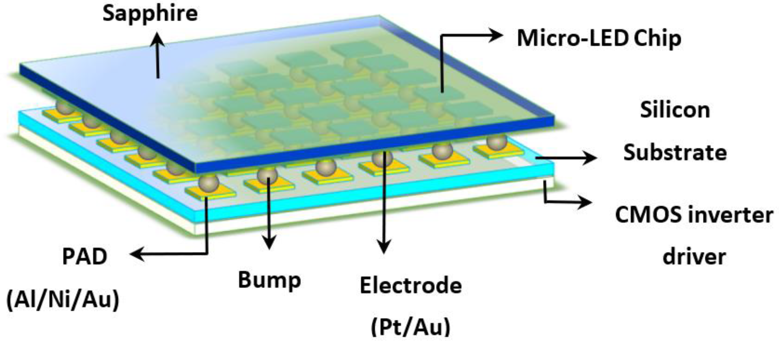
Figure 10–CMOS inverter driving micro-LED device model. The flip-chip bonding method is adopted, in which indium balls are used as solder, the CMOS inverter driver is located under the silicon substrate, the indium balls are connected with pads on the silicon substrate, and then the metal electrodes and micro-LED chips are connected, and sapphire is on the top.
The simulation results of PMOS, NMOS and CMOS inverters driving Micro-LEDs directly are shown in
Figure 11.
Figure 11a,b show the output characteristic curve. The green curve is the change curve of Micro-LEDs driven by NMOS. It can be seen that when the input level is low, the output voltage is less than 5 V, (about 2.2 V), and the current value through the micro-LED is close to 0 A (1.9275 pA). This is because the NMOS is not completely turned off at a low level, and current flows through it, and the equivalent resistance of NMOS is similar to that of the micro-LED at this time, which leads to the voltage division between the NMOS and the Micro-LED. When the input voltage is high, the NMOS is on, and the micro-LED has a large partial voltage, which makes the output voltage close to 0 V and the current through the micro-LED close to 90 mA. Therefore, the driving circuit forms the switching characteristics of low-level off and high-level on, but an NMOS driving micro-LED has the disadvantage of an incomplete low-level off. The red curve is the change curve of the PMOS driven Micro-LED. When the input level is low, PMOS is on, its output voltage is close to 5 V, and the current through the micro-LED is close to −90 mA. When the input voltage is high, its output voltage is less than 0 V (about 2.8 V), and the current value through the micro-LED is close to 0 A (−0.9679 pA). This is because the PMOS is not completely turned off at the high level, current flows through it, and the equivalent resistance of the NMOS is close to that of the Micro-LED, so the voltage division between the NMOS and the micro-LED is close. Therefore, the driving circuit has the switching characteristics of low-level on and high-level off, but the PMOS driving the micro-LED has the disadvantage of an incomplete high-level off. The blue curve is the change curve of the CMOS inverter driving the Micro-LED. Unlike the first two, in the circuit of the CMOS inverter driving the Micro-LED, the micro-LED device is located between the output terminal of the CMOS inverter and the ground level. Therefore, the micro-LED will not start until the output voltage reaches the micro-LED turn-on voltage. As can be seen from
Figure 11a, when the input voltage is about 2.644 V, the output voltage is 2.9 V, which reaches the turn-on voltage of the Micro-LED. Therefore, when the input voltage is low, the driving circuit is on, and the current value through the micro-LED is close to −90 mA; when the input voltage is high, the driving circuit is off, and the current value through the micro-LED is close to 0 A. Therefore, the driving circuit forms the switching characteristics of low-level on and high-level off, and the CMOS inverter driving the micro-LED does not have the problem of incomplete off.
In addition to judging the switching characteristics of the driving circuit according to the output characteristic curve, there is a relatively more important reference condition, that is, the rising time and falling time of the current in the transient characteristic curve. The smaller the sum of the two values, the steeper the rising edge and falling edge, the wider the signal bandwidth and the better the switching performance. The simulation results of transient characteristic curves of the micro-LED directly driven by PMOS, NMOS and CMOS inverters are shown in
Figure 12a,b. The input voltage is a trapezoidal pulse voltage curve. From
Figure 12b, it can be seen that three curves of current value passing through the micro-LED have rising edges and falling edges. Each curve of output current versus time is analyzed in more detail, that is, the rising time and falling time in the curve of output current versus time were analyzed.
Through the analysis of the graph simulation results of output current changing with time, we can get the rise time (tr), fall time (tf) and turn-on time (t) of the PMOS, NMOS and CMOS inverter driving circuits. The rise time (tr), is defined as the time value of 10–90% of the rise curve amplitude, the fall time (tf) is defined as the time value of 10–90% of the fall curve amplitude, and the turn-on time (t) is defined as the sum of the rise time (tr) and fall time (tf).
Figure 13 is the analysis of the process of rising time and falling time of the NMOS output current versus time.
Figure 14 is the analysis of the process of rising time and falling time of the PMOS output current versus time.
Figure 15 is the analysis of the process of rising time and falling time of the CMOS inverter output current versus time. According to the graphical analysis of simulation results, the rising time, t
r = 4.94 ps, and the falling time, t
f = 5.98 ps, t
N = t
r + t
f = 10.92 ps; rise time t
r = 3.0 ps and fall time t
f = 3.3 ps, t
P = t
r + t
f = 6.3 ps of the PMOS drive circuit; The rising time t
r = 5.45 ps and falling time t
f = 4.54 ps, t
C = t
r + t
f = 9.99 ps of the CMOS inverter driving circuit.
According to the results’ analysis, it can be found that the turn-on times of the micro-LED directly driven by the PMOS, NMOS and CMOS inverters are as follows: NMOS driver, CMOS inverter driver and PMOS driver.
The surge phenomenon can be clearly observed in the curves of the output current of the micro-LED directly driven by the PMOS, NMOS and CMOS inverters with time. Connecting a current limiting resistor in the circuit can solve this problem. At the same time, the current limiting resistor can reduce the current at the load end of the Micro-LED and prevent the device from being damaged by excessive current. In addition, the current limiting resistor can also play the role of voltage division. In the previous analysis of the simulation results, the NMOS driver has no advantage. Therefore, next, we analyzed the situation where the PMOS and CMOS inverters are connected with current-limiting resistors to drive the Micro-LED. Two driving circuit diagrams of Micro-LEDs with series current limiting resistors are shown in
Figure 16, and the resistance of the current limiting resistor is 10 KΩ.
Figure 17 is an analysis of the process of the rising time and falling time of the output current of the PMOS access current limiting resistor driving the micro-LED with time, and
Figure 18 is an analysis of the process of the rising time and falling time of the output current of the CMOS inverter access current limiting resistor driving the micro-LED with time. According to the graphical analysis of the simulation results, the rising time t
r = 5 ps, falling time t
f = 6.71 ps, t
N1 = t
r + t
f = 11.71 ps. The rising time t
r = 17.2 ps, falling time t
f = 17.2 ps, t
C1 = t
r + t
f = 34.4 ps when the CMOS inverter is connected to the current-limiting resistor in the driving circuit.
According to the result analysis, it can be found that the turn-on time of the micro-LED driven by an access current-limiting resistor from long to short is the CMOS inverter driving circuit and the PMOS driving circuit.
The PMOS, NMOS and CMOS inverter drive circuits, which directly drive the Micro-LED, have more advantages than driving the micro-LED with a current limiting resistor. In terms of switching characteristics caused by output characteristics, the CMOS inverter driving the micro-LED has greater advantages; the PMOS driving micro-LED circuit has greater advantages in switching characteristics caused by transient characteristics. Statistics of on/off times under different driving conditions are shown in
Table 3.


