Abstract
In this paper, an asynchronous and decoupled Hardware-In-the-Loop simulation of a DC nanogrid is presented. The DC nanogrid is a recent way to solve problems presented in traditional power generation, such as low efficiency, pollution, and cost increase. The complexity of this kind of system is high due to the interconnection of all the composing elements, making the use of HIL simulation attractive due to its advantages regarding computational power and low solution time. However, when a nanogrid is simulated in commercial and personalized platforms, all the elements presented are solved at the same integration time, even if some elements could be solved at smaller integration times, causing a slowdown of the system solution. The results of the asynchronous HIL simulation are compared with a synchronous HIL simulation with an integration time of 425 ns, and also with an offline simulation performed in PSIM software. The proposal achieves an integration time of 200 ns for the fastest element and 425 ns for the slowest, with an error of less than 0.2 A for current signals and less than 2 V for voltage signals. These results prove that the asynchronous and decoupled solution of an HIL simulation for nanogrid is possible, allowing each element to be solved as fast as possible without affecting the accuracy of the result, as well as simplifying programming.
1. Introduction
In recent years, the concept of distributed generation (DG) has been gaining attention due to its capability to mitigate the limitations of traditional power systems, mostly based on large-scale fossil-fueled generators. By using DG, power is generated close to the consumer, which reduces the size of transmission lines and consequently increases the efficiency and reliability of the system [1].
To use DG, the concept of nanogrid (NG) is gaining more and more attention worldwide. An NG is a power distribution system for a single house or small building, with the ability to connect or disconnect from other power entities via a gateway [2]. NG is mainly classified as AC or DC ones, according to the kind of power used by the bus that interconnects all its components. Both topologies have their benefits and drawbacks, and the selection depends on the NG application and its ultimate purpose. For instance, in a case where the system’s efficiency is of utmost importance, a DC topology is more suitable, as one power conversion stage is omitted [3]. Currently, AC topology is most commonly adopted, a decision mainly driven by financial reasons. As most electrical appliances in the market are supplied from AC power, retrofitting an existing building with DC loads would increase the cost of the NG infrastructure.
The typical structure of a DC NG distribution system is depicted in Figure 1. It consists of renewable energy sources (RES), energy storage systems, loads, and a gateway to interface with other power entities, such as adjacent NG or Microgrids (MG) and the power grid.
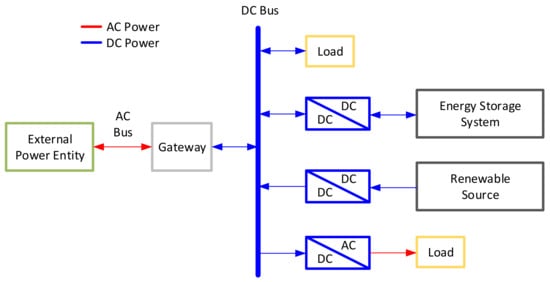
Figure 1.
Typical structure of DC nanogrid.
To develop an NG, the simulation plays an important role, as it permits safely testing the NG and studying particular scenarios that are difficult to recreate in a real NG. The Hardware In the Loop (HIL) is a technique where actual signals from a controller are fed into a test system that simulates the behavior of a real system. The test system typically runs a mathematical model of the system to be controlled on a real-time digital device, such as an FPGA, a microprocessor, or a DSP.
To simulate complex models as an NG, commercial HIL equipment is often used. Its main disadvantages are its high cost and the integration time (ti) that can be obtained in the range of 0.5 to 2 µs [4]. This ti limits the switching frequency of power converters to around 20 kHz. When the simulation of an NG is executed in commercial hardware, all the element models are solved at the same ti. In recent years, some researchers have started implementing complex models for HIL simulation using FPGA due to their inherent parallelism and low latency.
In [5,6,7,8,9,10], commercial hardware simulates DC or AC MG. In these references, the main goal is to prove novel controllers for the power exchange between the main grid and MG.
Many efforts have been made to simulate MG using FPGAs. In [4], a method that allows simulating an AC MG using a low-cost FPGA is presented, which proposes a strategy that simulates the models of the converters in Real-Time in less than a microsecond, using a decoupling method between the elements. However, all models must be solved using the same ti, even when some elements could be solved more quickly.
Another method to simulate complex systems using decoupled methods can be seen in [11], based on using Zhen’s method [12]. This method consists of converting elements into current and voltage sources, for example, inductors as current sources and capacitors as voltage sources. A more electric plane is used as a case study. However, it is not mentioned whether the ti used in the simulation and the whole system is solved using the same ti.
Another strategy to simulate MGs in FPGA is observed in [13,14], where using an FPGA is proposed to simulate systems with several elements, such as MG. The models of each of the MG elements are implemented in different FPGAs, generating larger systems. However, a synchronization signal should be used between the different FPGAs, and all systems are solved at the same ti.
In this paper, an asynchronous and decoupled method to simulate NG is presented. This method allows simulating and evaluating each component of an NG independently, using the minimum ti for each component, resulting in an accurate simulation for each NG element and the whole NG. The RES systems are decoupled with each other and simulated in parallel so that new RES integrations can be easily achieved; the main novelty of this proposal is the possibility of using different integration times in different parts of the system. In addition, it makes possible the simulation of power converters at different commutation frequencies, which are no longer limited due to the ti of the slowest simulated element. The type of simulation presented in this work achieves results more similar to what happens while implementing a physical NG. Also, the implementation of this simulation is easier than others because a synchronization signal is not required.
This paper is organized as follows; in Section 2, the main idea to perform the HIL simulation of an NG is depicted. Section 3 shows the modeling of all the elements that constitute the NG and its implementation in the FPGA. Section 4 shows the results obtained from the asynchronous HIL simulation compared to an offline simulation and a synchronous HIL simulation, and finally, Section 5 presents our conclusions.
2. Proposed HIL Simulation for NG
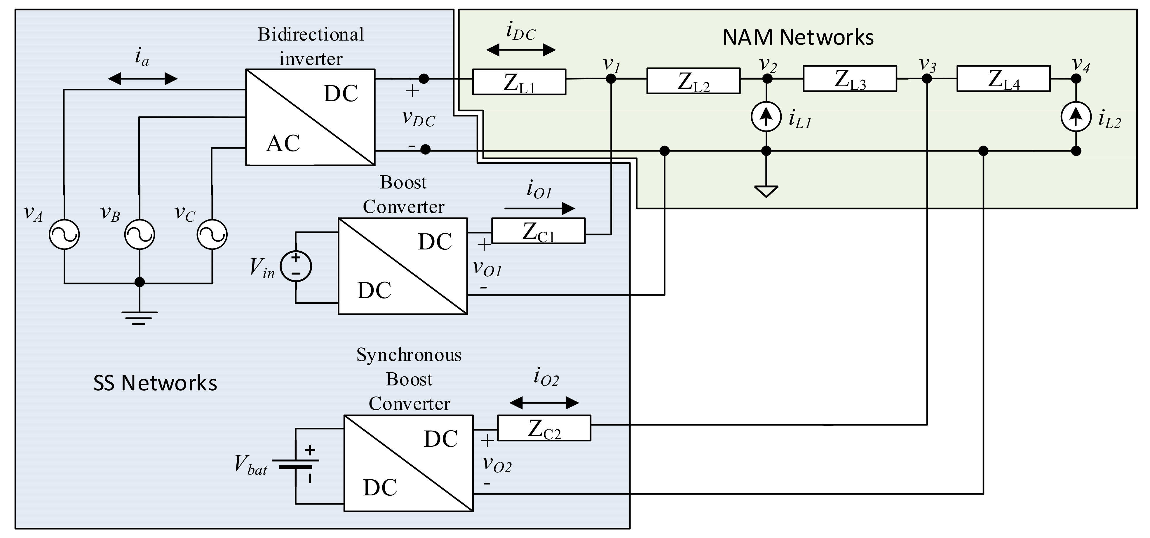
Traditionally, the nodal analysis method (NAM) is used as the solution method in commercial HIL simulation hardware. As it is well known, this forces using a single ti to solve the whole system. As a result, the actual execution time and the FPGA resource consumption will increase quickly as the complexity of the system increases. Unlike the centralized NAM used in commercial hardware, the main objective of this proposal is to decouple an NG in several submodules. In this way, each module can be solved as fast as possible and with different solution methods, if required, such as state-space (SS) or NAM.
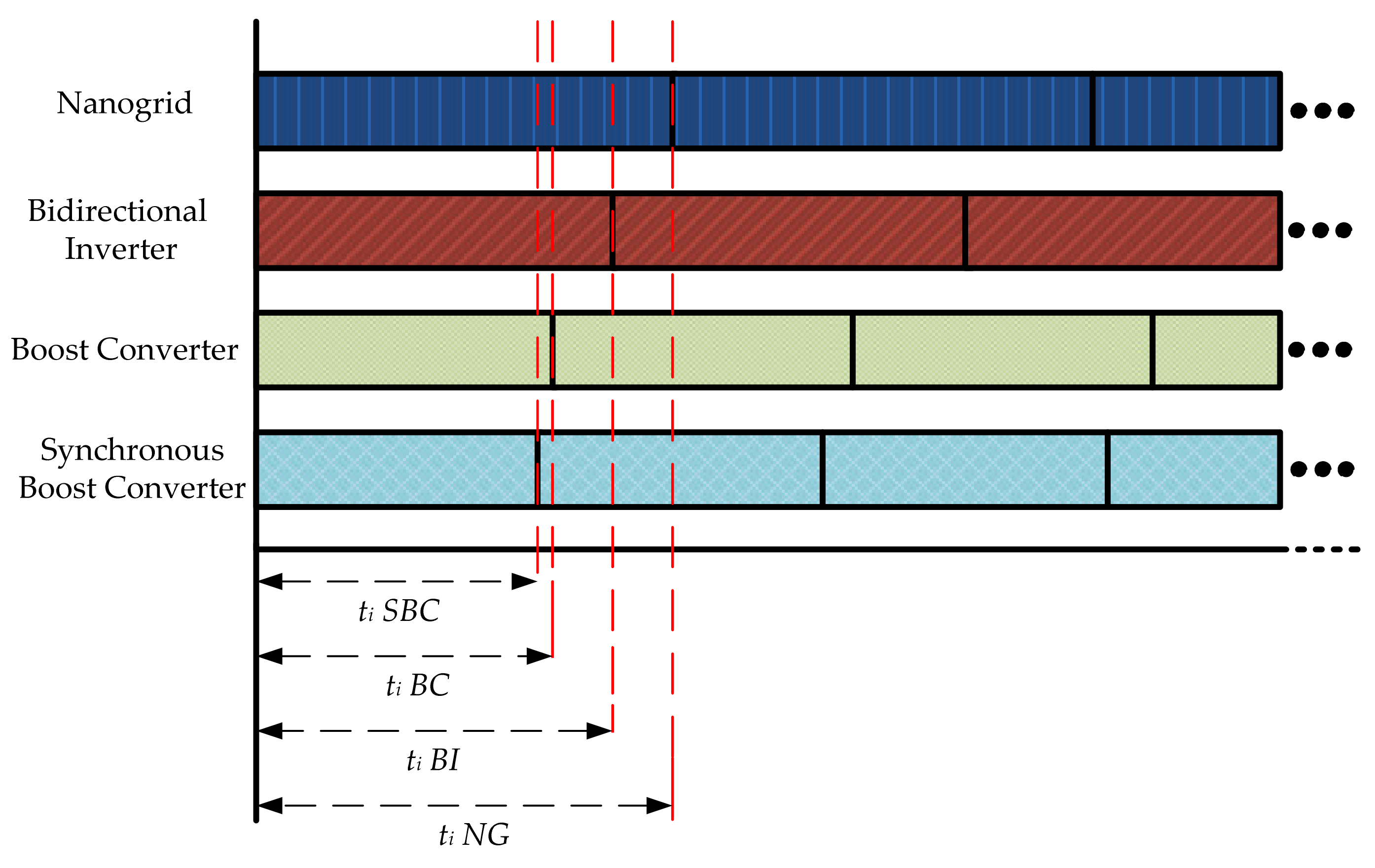
Therefore, a hybrid solution is obtained to perform the real-time simulation of an NG, as shown in Figure 2. The power converters in DG systems (including the energy storage systems) are modeled using state spaces and solved with the Euler method, from now on referred to as the SS networks in this paper. The distribution lines are modeled with NAM, and are called the NAM network. Both the SS and the NAM networks are solved asynchronously (Figure 3), allowing each element of the NG to be solved at a minimum ti. It is important to notice that other solution methods can be used to solve the different systems.
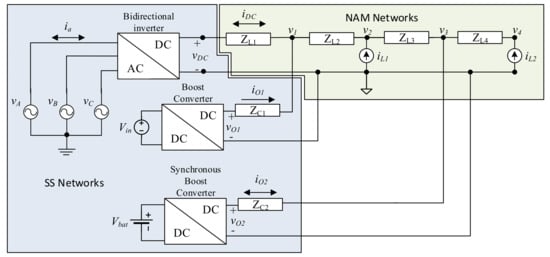
Figure 2.
DC NG proposed topology, the power electronic converters are solved using SS, and the NG is solved using NAM.
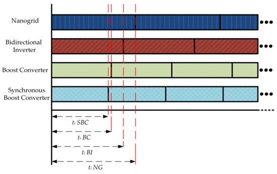
Figure 3.
Asynchronous solution of DC NG.
3. Methodology
3.1. DC Nanogrid Topology
Figure 2 shows the DC NG topology proposed in this paper, derived from that presented in [15]. It consists of: a boost converter (BC) connected to a RES that supplies DC power, its voltage is represented as Vin; a synchronous boost converter (SBC) connected to a battery with a voltage Vbat; a bidirectional power inverter (BI) that works as a gateway between the grid and the DC bus, and two loads represented as current sources iL1 and iL2. The impedances between components are included as well.
3.2. DC Nanogrid Model
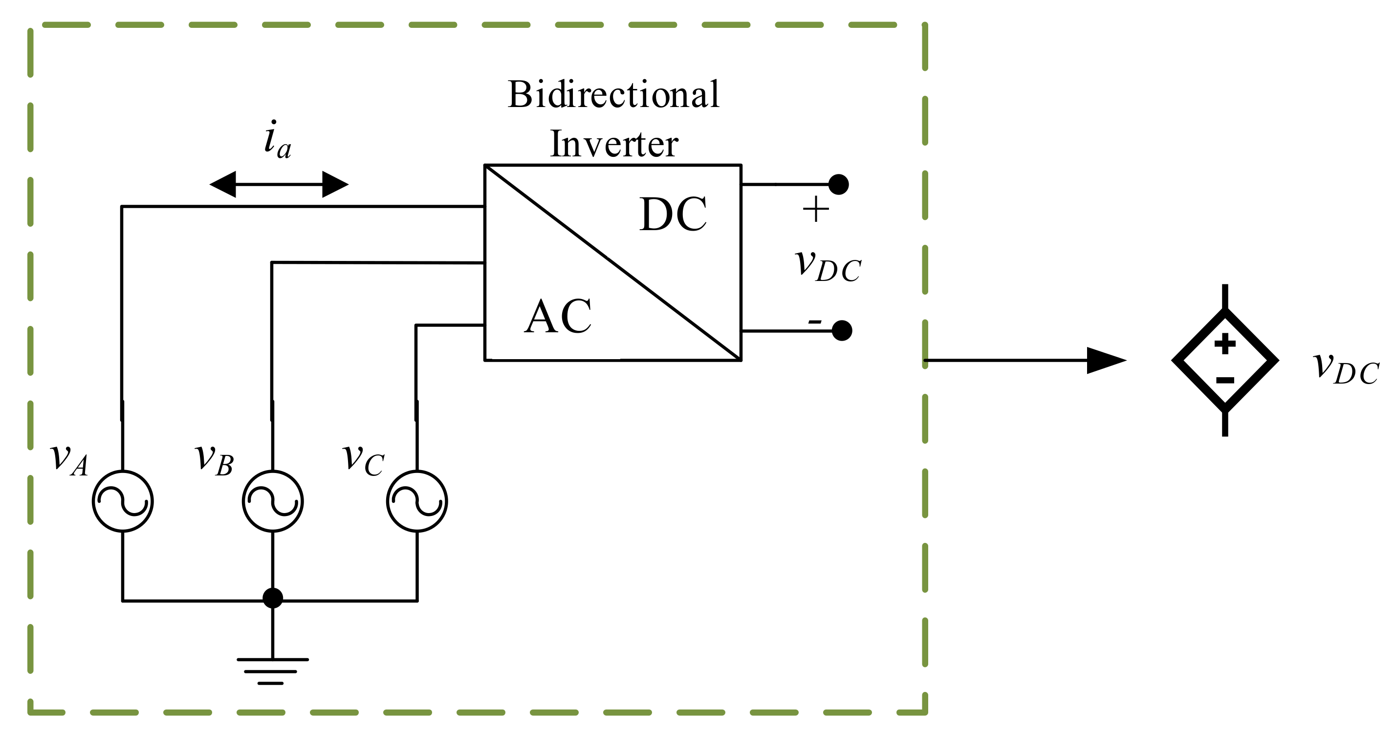
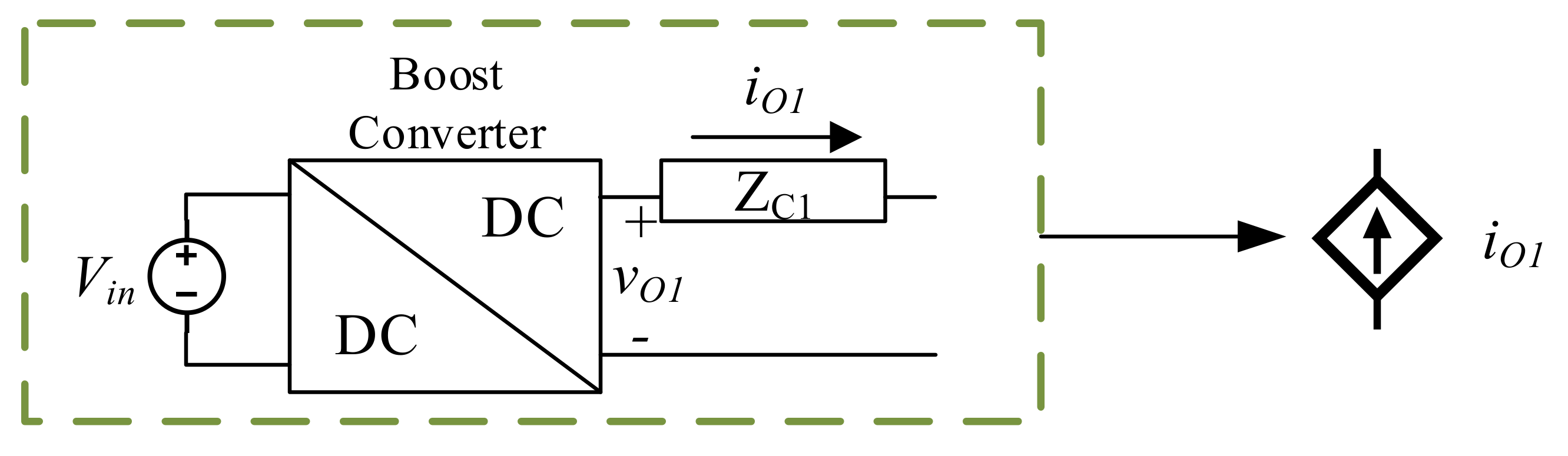
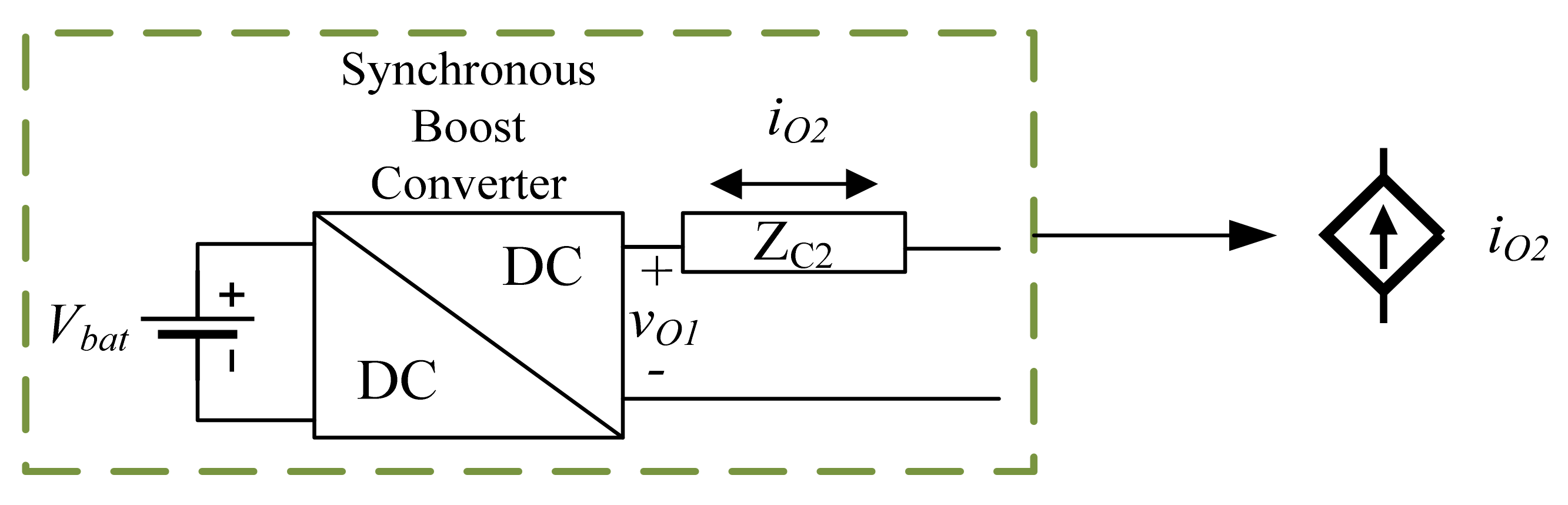
To model the DC NG, dependent power supplies replace the DC-DC converters and the bidirectional inverter, which is replaced by a DC voltage power supply with vDC value (Figure 4) since its main function is to regulate the DC bus voltage. The DC-DC converters and their impedance associated with the connection to the NG are replaced by two dependent DC power supplies, iO1, and iO2 (Figure 5 and Figure 6). Finally, two independent DC power supplies replace the loads. It is important to notice that the values of the dependent power supplies are continuously solved using their models.
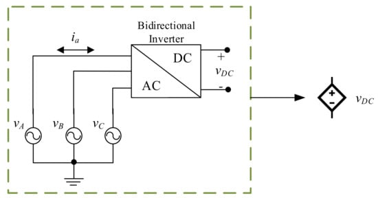
Figure 4.
Equivalent DC voltage power supply for BI.
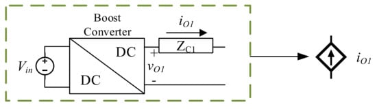
Figure 5.
Equivalent DC power supply for BC.
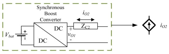
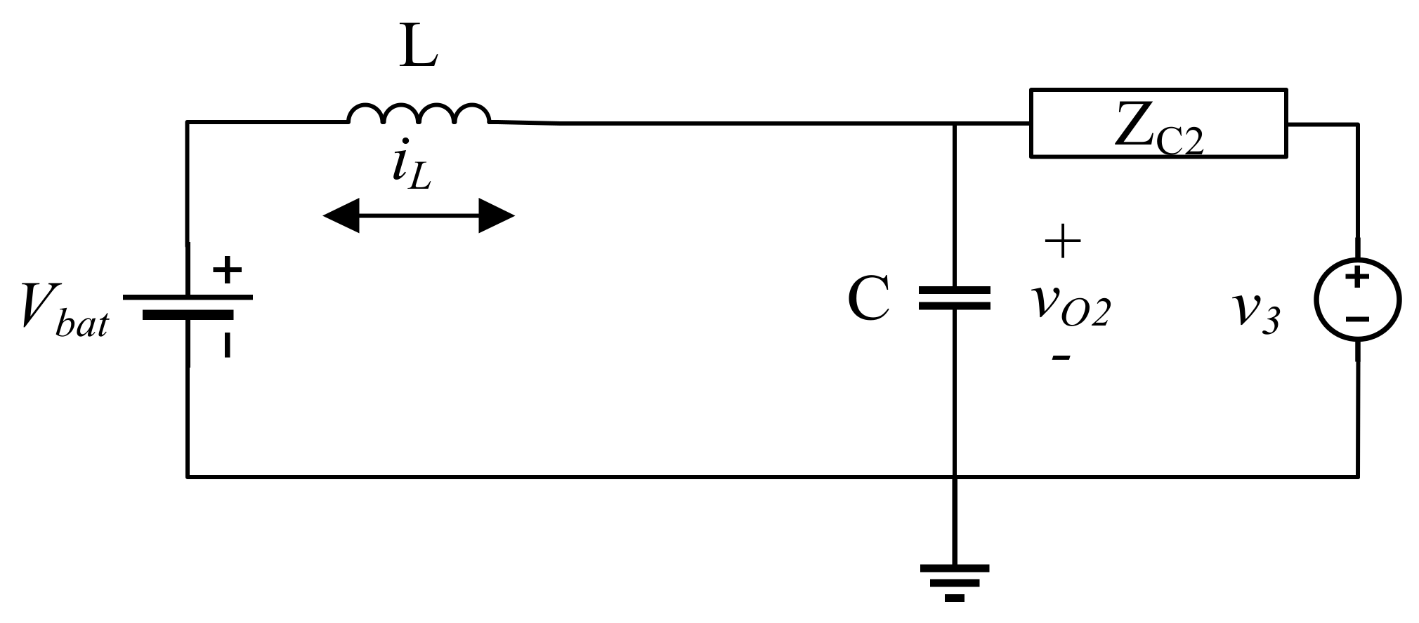
Figure 6.
Equivalent DC power supply for SBC.
From Figure 2, iO1 and iO2 can be obtained by using:
where iOx is the converter output current, vOx is the converter output voltage, vx is the node voltage where the converter is connected to the NG, and ZCx is the impedance between the NG and the DC/DC converter.
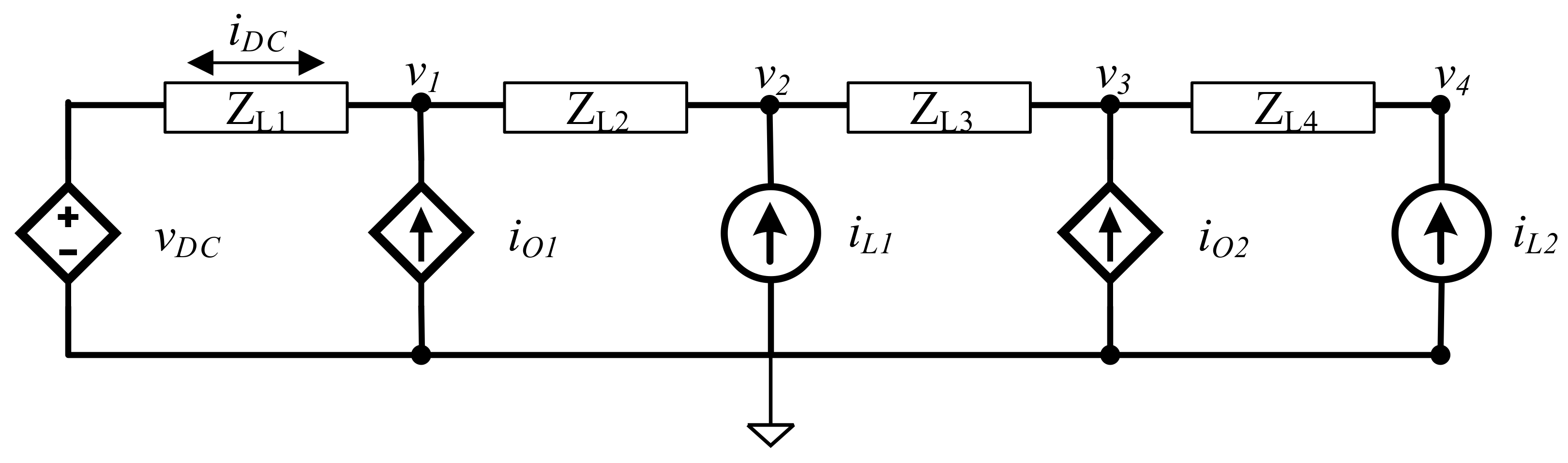
Using the replacements from Figure 4, Figure 5 and Figure 6, an equivalent circuit of the DC NG is obtained (Figure 7). The mathematical model is obtained using classic circuit analysis techniques.
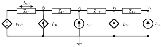
Figure 7.
DC NG equivalent circuit.
Taking the circuit in Figure 7 and applying Kirchhoff’s current law, it is possible to find the voltage in each node of the NG. The matrix representation of the system, considering that all the impedances between the NG nodes (ZLx) are equal, can be written as:
It can be observed from Figure 7 that:
Equation (2) is of the form:
where:
The solution of (4) is given by:
It is important to note that matrix Y is time-invariant, and values for the j vector are easily obtained from (1).
3.3. Power Converter Models
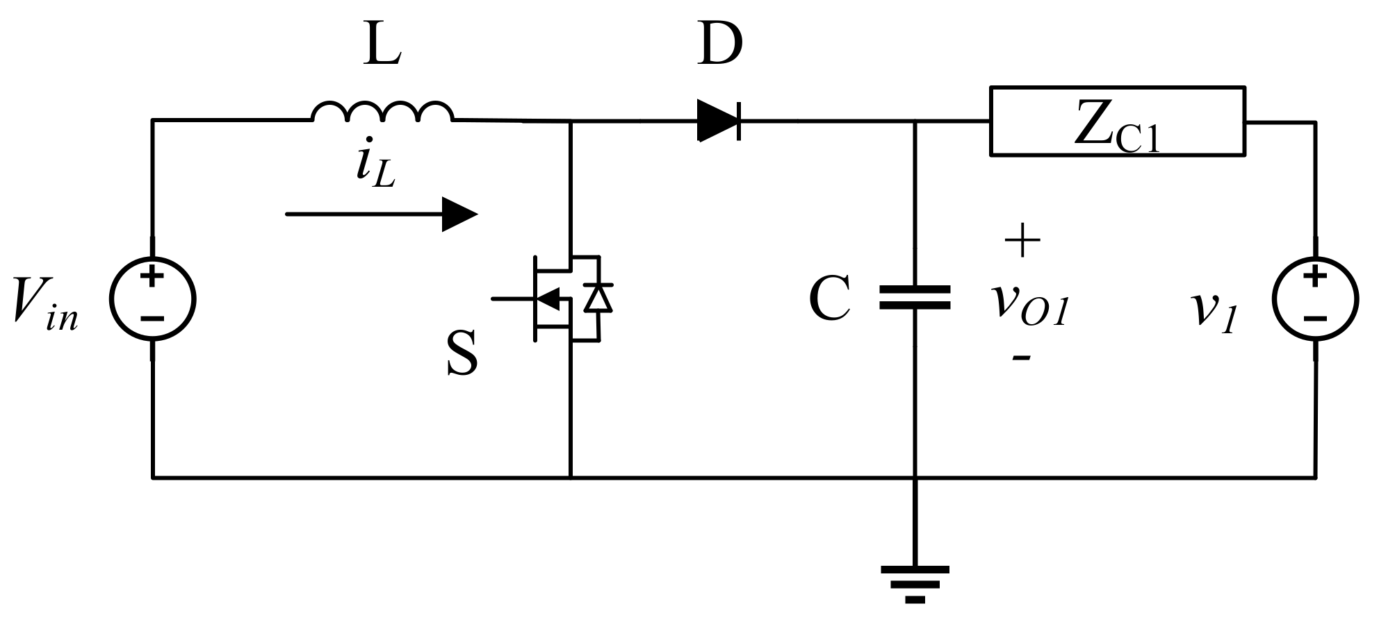
Figure 8 shows the boost converter. This converter presents three states according to switch (S) and the current through the inductor (iL). The first state occurs when S is on, causing an iL increase, and the diode D is open (Figure 9). The second state is when S is off, causing D to close and iL to start to decrease (Figure 10). The third state occurs when S is off and the inductor (L) is fully discharged, so in this state iL = 0 (Figure 11).
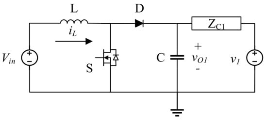
Figure 8.
Schematic circuit of Boost Converter.
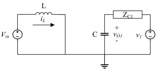
Figure 9.
Schematic circuit of Boost Converter for the first state (S = 1).
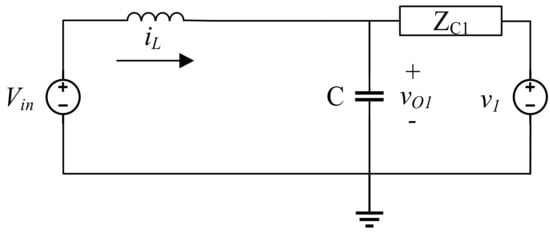
Figure 10.
Schematic circuit of Boost Converter for the second state (S = 0).
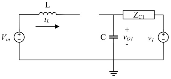
Figure 11.
Schematic circuit of Boost Converter for the third state (S = 0 and iL = 0).
Using circuits from Figure 9, Figure 10 and Figure 11 and using Kirchoff’s Laws, the differential equations that model the converter can be obtained and then solved by the Euler method.
The differential equations for the first state are given by:
where Vin is the input voltage of the BC, vO1 is the output voltage of the BC, C is the output capacitor, ZC1 is the impedance between the converter and the NG, and v1 is the node where the converter is connected to the NG.
Solving (6) using the Euler method, the difference equations are given by:
For the second state, the differential equations are given by:
Solving (8) using the Euler method, the difference equations are given by:
For the third state, the differential equations are given by:
Solving (10) using the Euler method, the difference equations are given by:
Figure 12 shows the synchronous boost converter. As it can be noticed, both semiconductors are controlled switches, that being the main difference compared to the asynchronous boost converter seen before. The advantage of doing so is that it permits the power flow to be bidirectional, while the asynchronous boost only permits power flow to the right. This bidirectional power transfer is commonly used to charge and discharge batteries.
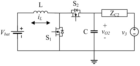
Figure 12.
Schematic circuit of Synchronous Boost Converter.
This converter presents two states according to switches S1 and S2. The equivalent circuits for the converter states are shown in Figure 13 and Figure 14.
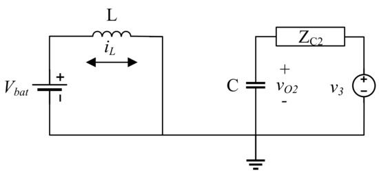
Figure 13.
Schematic circuit of Synchronous Boost Converter for the first state (S1 = 1 and S2 = 0).
Figure 14.
Schematic circuit of Synchronous Boost Converter for the second state (S1 = 0 and S2 = 1).
The differential equations associated with the circuit in Figure 13 are:
where Vbat is the battery voltage, vO2 is the output voltage of the SBC, ZC2 is the impedance between the converter and the NG, and v3 is the connection node between the NG and the converter.
Solving (12) using the Euler method, the difference equations are given by:
The differential equations associated with the circuit in Figure 14 are:
Solving (14) using the Euler method, the difference equations are given by:
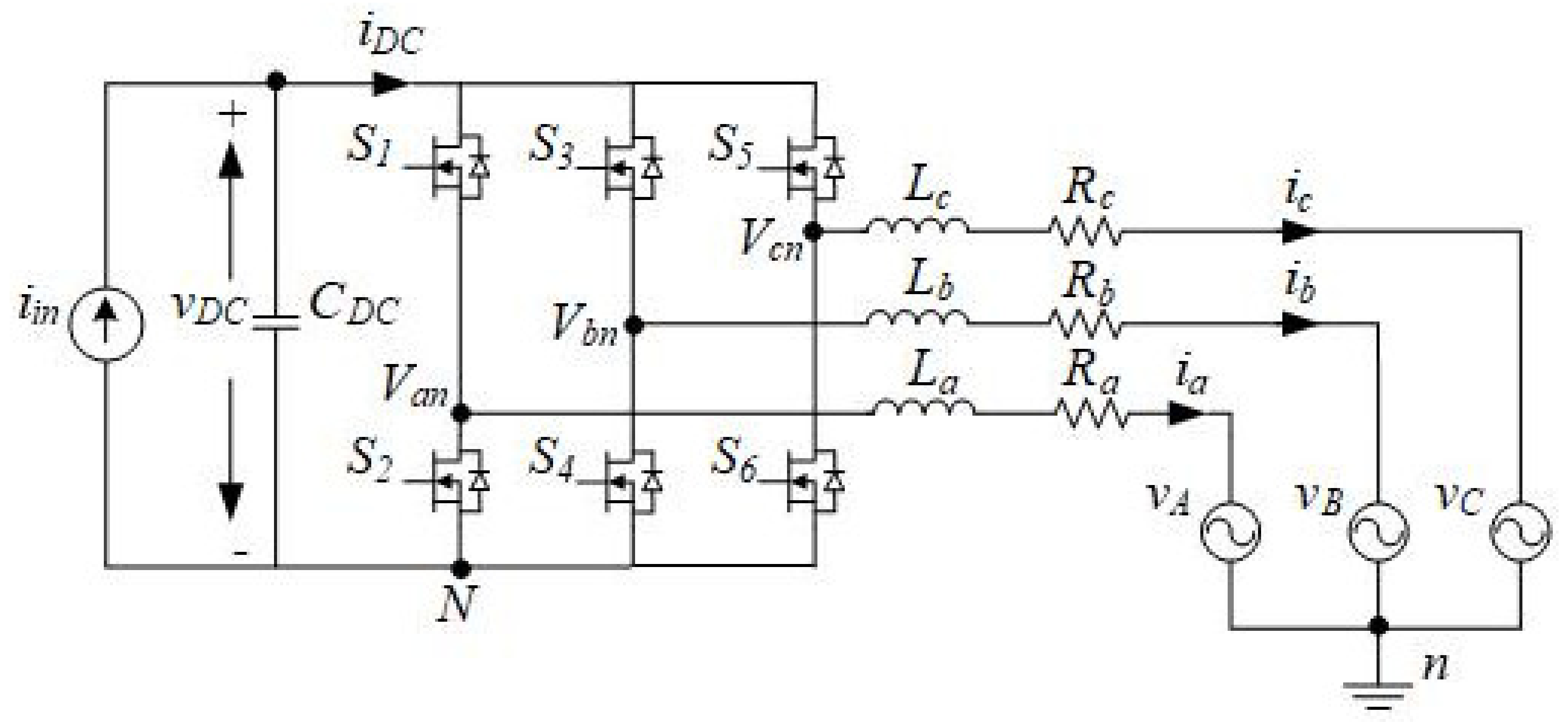
Figure 15 shows the bidirectional inverter used as a gateway between the NG and the AC mains.
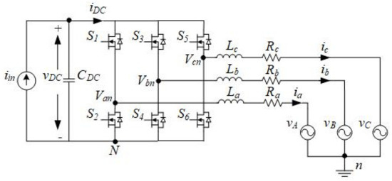
Figure 15.
Schematic circuit of the Bidirectional Inverter.
The detailed model of the bidirectional inverter can be found in [16]. The difference equations associated with this converter are:
where vxn is the phase ‘x’ inverter voltage, vX is the phase ‘X’ grid voltage, ix is the phase ‘x’ inverter current, Lx is the inductance of the topology, Rx is the series inductor resistance, vDC is the capacitor voltage, CDC is the DC-side capacitor, iDC is the current demanded by the inverter, and iin is the MG current.
The obtained difference equations are easily implemented in high-level programming languages such as LabVIEW.
3.4. FPGA Implementation
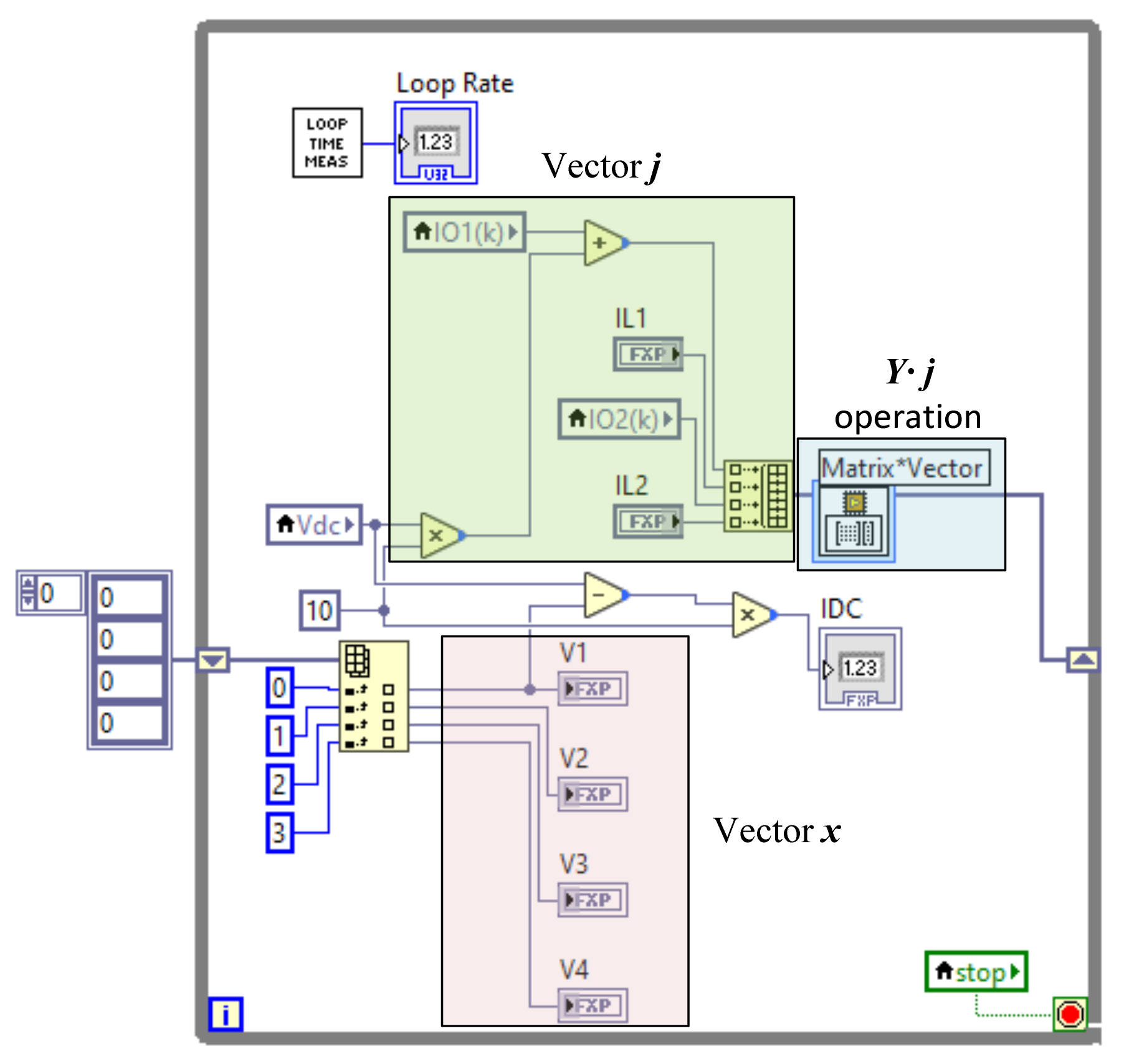
The methodology presented in [17] is used for the FPGA implementation. Figure 16 shows the implementation of the NG model. The j vector and the solution to the Y∙j operation can be observed, carried out with a predefined LabVIEW function. It is also important to notice that the matrix Y is generated offline and is time-invariant. The voltage values from the NG are obtained using the current values that each model converter provides. The DC NG model presented in Figure 16 has a different ti than the models of the converters, creating a complete asynchronous solution.
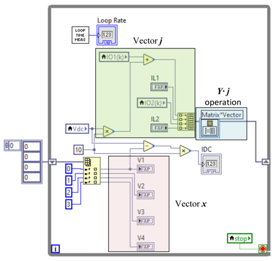
Figure 16.
LabVIEW FPGA NG implementation.
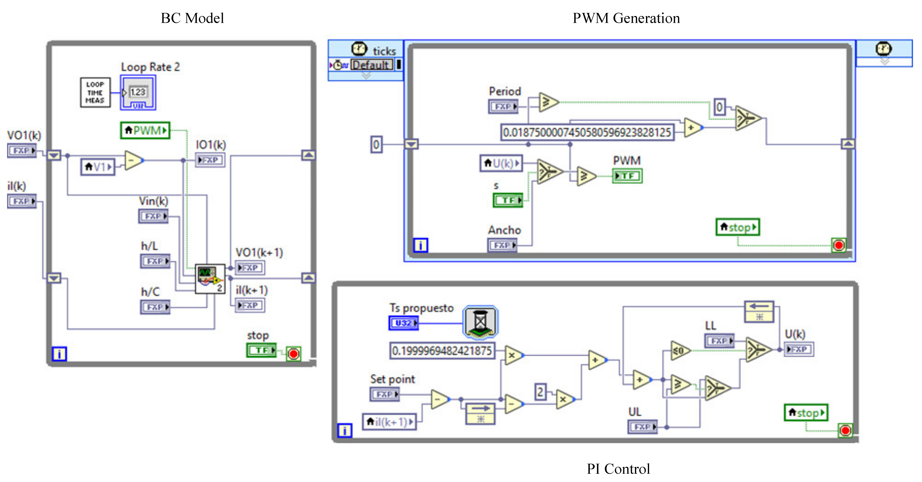
Figure 17 shows the implementation of the boost converter, the PI regulator used to control its output current (iO1), and the generation of the PWM signal.
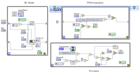
Figure 17.
LabVIEW FPGA implementation of the boost converter, PI control, and PWM signal.
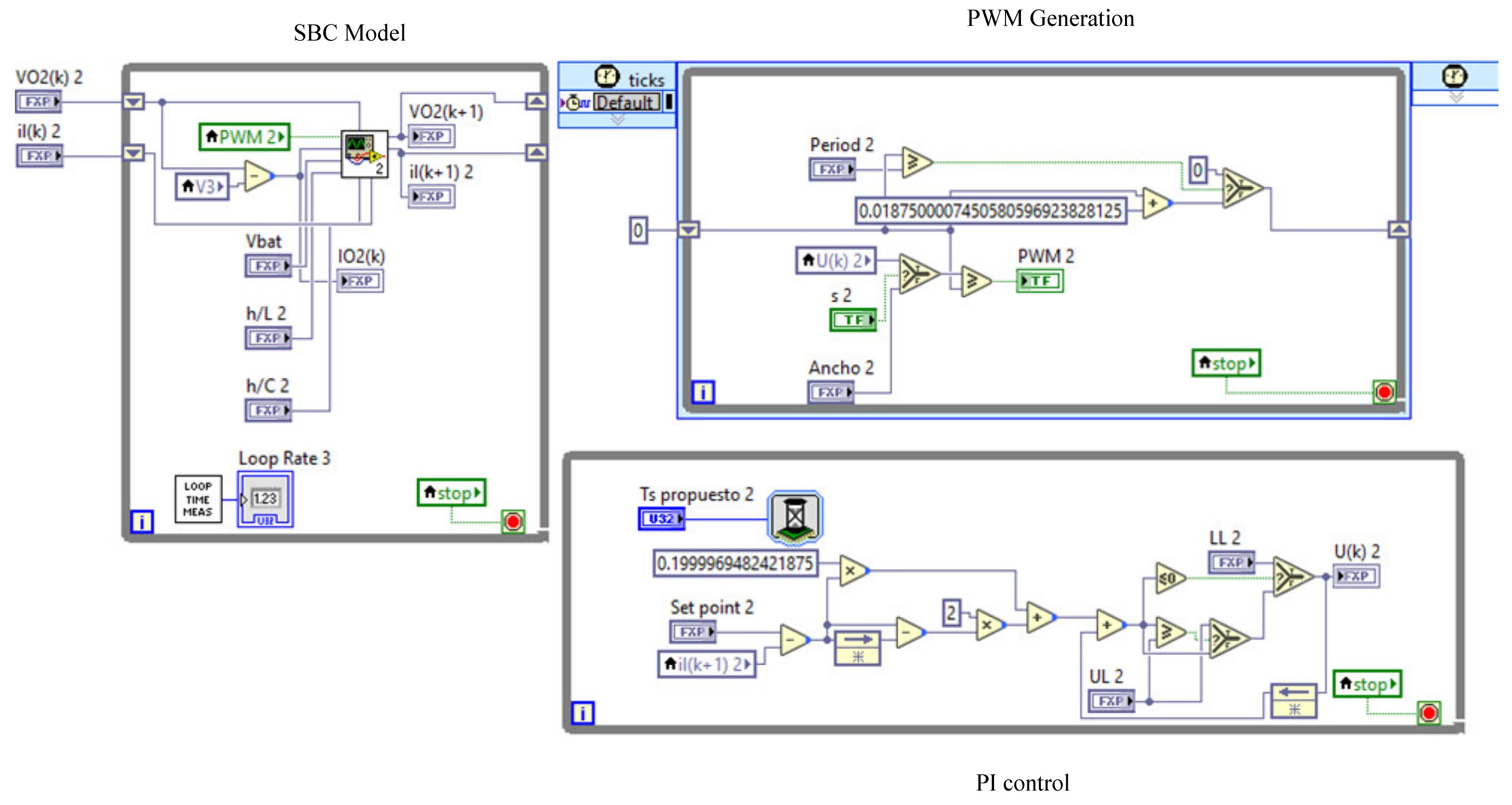
Figure 18 shows the implementation of the synchronous boost converter, the PI regulator used to control its output current (iO2), and the generation of the PWM signal.
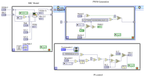
Figure 18.
LabVIEW FPGA implementation of the synchronous boost converter, PI control, and PWM signal.
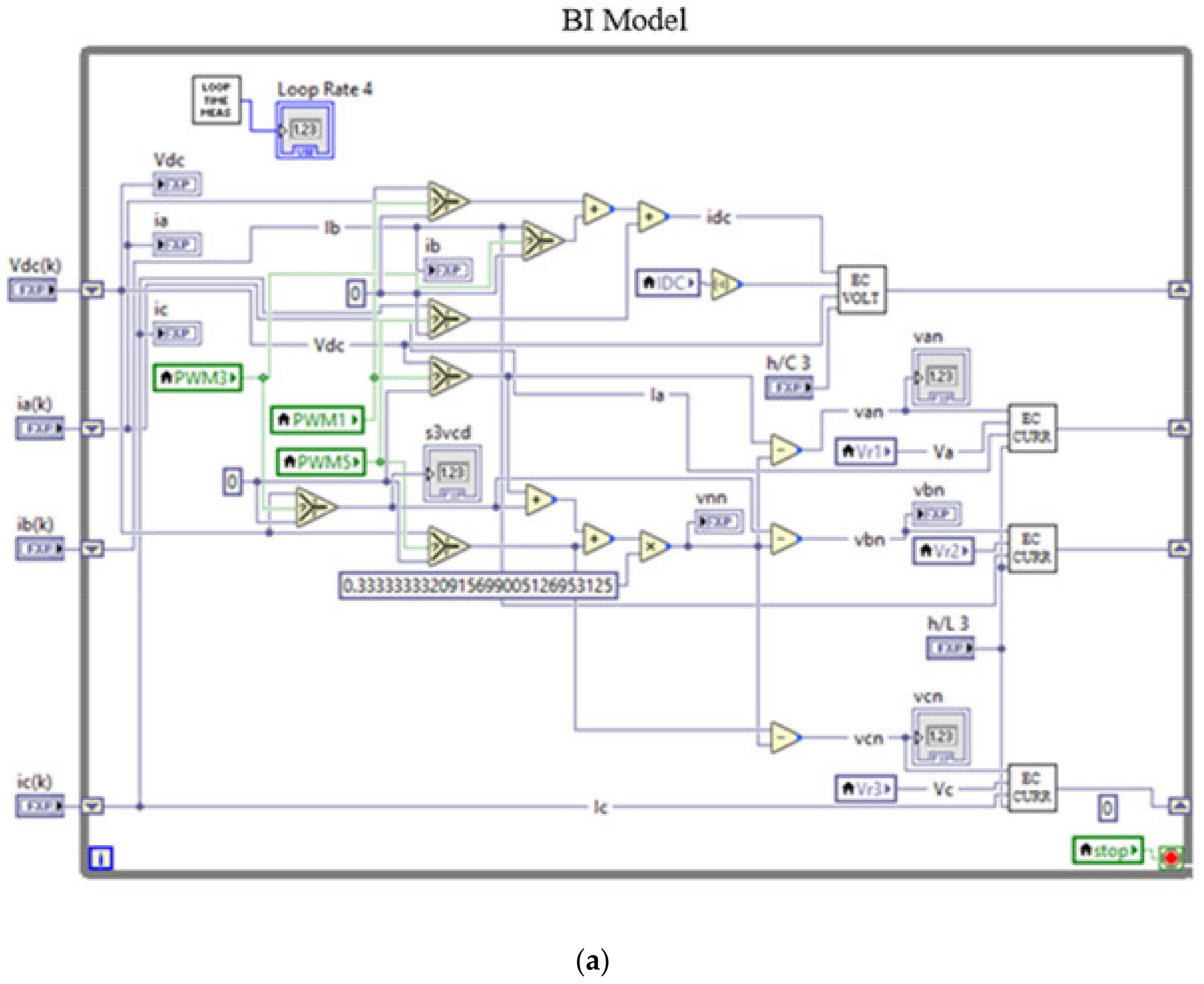
Figure 19 shows the implementation of the BI model, the generation of the three-phase power supply signals, and the control used for this converter based on [16].
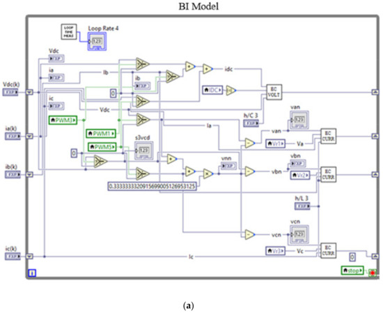

Figure 19.
LabVIEW FPGA implementation (a) the bidirectional inverter, (b) the three-phase power signals, and (c) control.
Figure 16, Figure 17, Figure 18 and Figure 19 clearly show the decoupling of each element that makes up the NG. This feature is important since the NG can be developed modularly, which is desirable in large applications. The output currents of the converters are sent to the NG model through shared variables. The NG model is responsible for obtaining the voltages of the nodes to which the different elements are connected. Figure 20 shows the graphical user interface (GUI) of the HIL simulation for NG. In the interface, the parameters of the NG, such as the current of the loads, can be modified in Real-Time. Parameters and passive elements of the converters and inverter can also be adjusted.
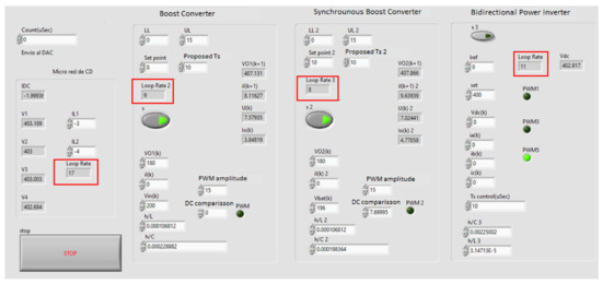
Figure 20.
GUI of the HIL simulation of NG.
Figure 20 shows the controls for adjusting the parameters of the DC-DC converters, and the clock cycles it takes to execute each element using the Loop Rate indicator. Table 1 shows the clock cycles of each element, which is the smallest number of cycles obtained from the implementation of the element models in the FPGA using the methodology in [17]. It is important to mention that the hardware used for the HIL implementation is a NI cRIO-9067 with a Zynq-7020 FPGA, which has a clock frequency of 40 MHz.

Table 1.
Clock cycles and time for each element in NG.
4. Results
In this section, the results from the asynchronous HIL NG simulation are presented. Its performance is compared against an offline simulation using PSIM software and a synchronous HIL NG simulation using a ti = 425 ns, which is the larger ti shown in Table 1 (corresponding to the NG). In Table 2, the parameters of the NG are presented. A resistive behavior of ZL is considered to simplify the calculations.
Table 2.
DC NG parameters.
The boost and the synchronous boost converter were designed using the methodology presented in [18]. The design parameters are presented in Table 3 and Table 4, respectively.
Table 3.
Design parameters for the boost converter.
Table 4.
Design parameters for the synchronous boost converter.
The calculated passive elements for both converters are shown in Table 5.
Table 5.
Passive elements for both converters.
Three tests were conducted to verify the behavior of the simulation. In the first one, the current reference for the boost converter increases while the other parameters are maintained without change. In the second test, a change in current reference for synchronous boost converted is made, first supplying energy to the NG and later consuming energy from the NG. In the third test, the current of one load is increased. The synchronous and asynchronous HIL simulation signals are obtained through an oscilloscope; that is, they are sent from the simulation to the real world through a digital to analog converter.
During the tests, four signals are obtained. One is the signal with the value changing, and another is iDC to demonstrate that the NG is supplying or consuming energy from the main grid (a negative value indicates that the NG is supplying energy and a positive value indicates that it is consuming energy from the NG). Signal ia demonstrates that the bidirectional inverter is generating a sinusoidal waveform, and the phase is also used to determine whether the NG is supplying or consuming energy. The final signal is vDC, the voltage of the DC bus. This signal is shown to demonstrate the stability of the NG, its value has to be near 400 V, and that is expected to increase when the NG is supplying energy and decrease when it is consuming energy.
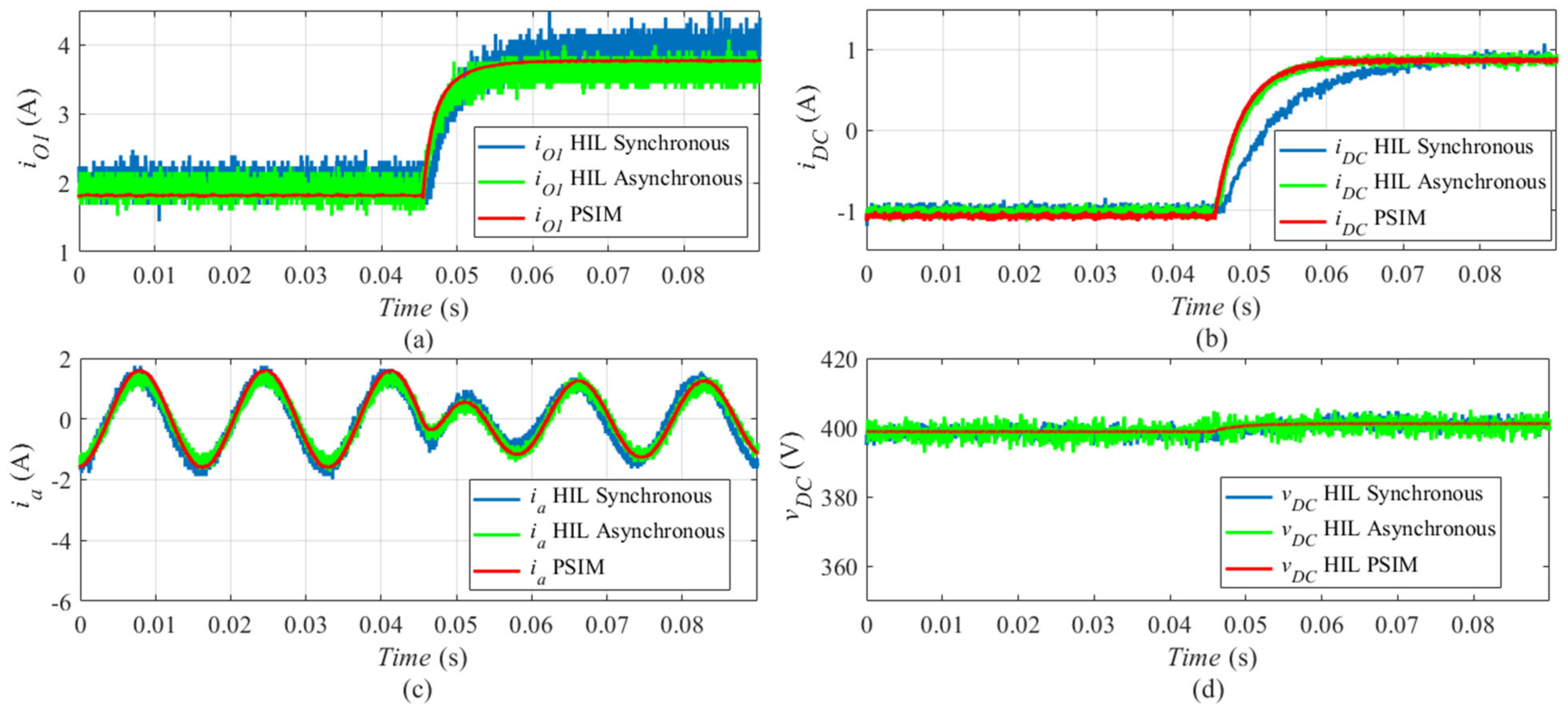
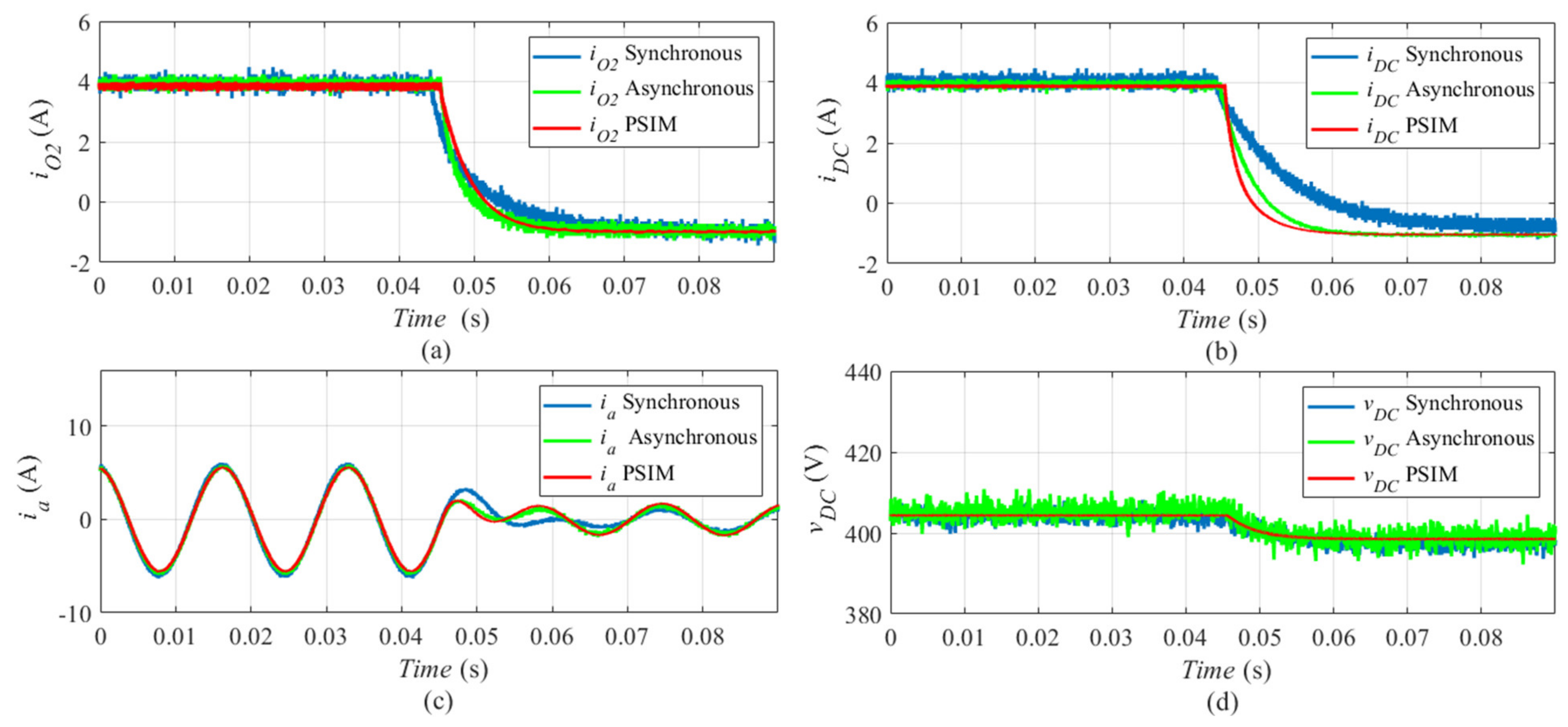
In Figure 21, a comparison between HIL simulations and offline simulations for the first test is shown. In Figure 21a, the current reference iO1 changes from 2 A to 4 A. In Figure 21b, the iDC current changes from −1 A to 1 A. In Figure 21c, it can be observed a magnitude and phase change in current ia, denoting that in one instant the bidirectional inverter is supplying energy and later is receiving it. In Figure 21d, the vDC voltage is observed. This test was performed with an iL1 and iL2 equal to 3 A, while iO2 supplies a current of 3 A.

Figure 21.
First test results of HIL simulations and PSIM, (a) iO1, (b) iDC, (c) ia and (d) vDC.
Table 6 compares the three simulations using the mean absolute error (MAE). It can be noticed that the behavior is similar between simulations; however, a smaller error is obtained with asynchronous HIL simulation.
Table 6.
First test comparison between the PSIM and HIL simulations.
In Figure 22 comparison between three simulations for the second test is shown. In Figure 22a, the current reference iO2 changes from 4 A to −1 A. In Figure 22b, it can be noticed the iDC current changes from 4 A to −1 A. In Figure 22c, it can be observed a magnitude and phase change in current ia, denoting that in one instant the bidirectional inverter is supplying energy and later is receiving it. In Figure 22d, the vDC voltage is observed. This test was performed with an iL1 and iL2 equal to 3 A, while iO1 supplies a current of 6 A.
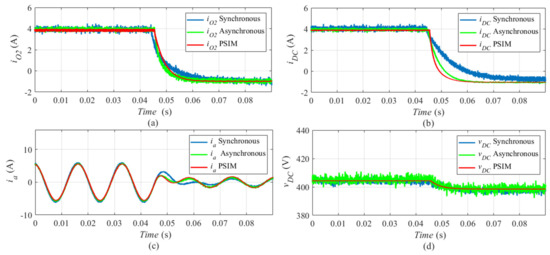
Figure 22.
Second test Results of HIL simulations and PSIM, (a) iO2, (b) iDC, (c) ia and (d) vDC.
Table 7 shows a comparison between the PSIM and HIL simulations using MAE. It can be noticed that the behavior is similar between simulations. Again, the error is smaller in the asynchronous HIL simulation.
Table 7.
Second test comparison between the PSIM and HIL simulations.
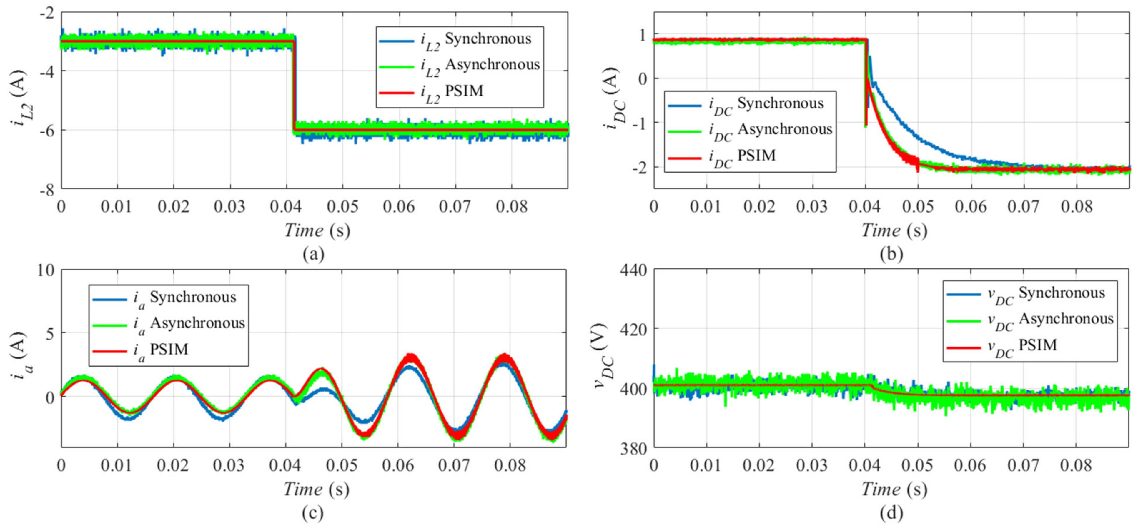
In Figure 23 comparison between HIL simulations and PSIM for the third test is shown. In Figure 23a, the current iL2 is shown, changing from 3 A to 6 A. In Figure 23b, it can be noticed the iDC current changes from 1 A to −2 A. In Figure 23c, it can be observed the magnitude and phase in current ia, denoting that in one instant the bidirectional inverter is supplying energy and later is receiving it. In Figure 23d, the vDC voltage is observed. This test was performed with an iO1 = 4 A and iO2 = 3 A, while iL1 demands a current of 3 A.

Figure 23.
Third test Results of HIL simulations and PSIM, (a) iL2, (b) iDC, (c) ia, and (d) vDC.
Table 8 shows a comparison between the PSIM and HIL simulations. It can be noticed that the behavior is similar between simulations, but the smaller error is presented in the asynchronous HIL simulation.
Table 8.
Third test comparison between the PSIM and HIL simulation.
The results presented in Figure 21, Figure 22 and Figure 23 prove that the behavior between PSIM and HIL simulations is similar. However, it is important to notice that the ti for PSIM simulation is 200 ns, fixed for all the elements, and that the simulation with the lesser error is the asynchronous HIL simulation. Furthermore, the asynchronous HIL simulation shows, at minimum, the same precision as the PSIM simulation. This proves that the asynchronous HIL simulation can be used to test control systems for the power converters and energy management systems for the NG in a more realistic scenario since they usually have an asynchronous operation.
5. Conclusions
Nowadays, DC NG is gaining importance worldwide. These systems are complex, so simulation plays a major role in their implementation. Regarding simulation, there is no doubt that HIL simulation has substantial advantages over offline simulation. However, performing simulations of a DC NG using commercial hardware forces the system to be solved in the same integration time. Custom solutions offer advantages, but also force the system to be solved in the same integration time.
The implementation of a DC NG was achieved modularly and with different integration times for each element, that is, asynchronously. This implies advantages over other implementations that require the synchronization of all the elements, slowing down the general system, and also provides a more realistic operation than the actual systems since they may operate asynchronously in reality. The main novelty of this proposal is the possibility of using different integration times in different parts of the system.
The NG model was obtained by replacing each element with an equivalent circuit (voltage or current source) to model the NG using nodal analysis techniques. The converters used in the NG (bidirectional inverter, boost converter, and synchronous boost converter) were also modeled using the state spaces approach.
The implementation of each element in the FPGA was presented using the LabVIEW FPGA software, which helps make the implementation easier than using other low-level languages through using its own functions and, at the same time, with the power of implementing custom-made models.
Tests were performed on the DC NG. The results of the asynchronous HIL simulation are compared with a synchronous HIL simulation having an integration time of 425 ns, and with an offline simulation performed in PSIM software, achieving an integration time of 200 ns for the fastest element and a 425 ns in the slowest element. The error obtained is less than 0.2 A for current signals and less than 2 V for voltage signals. The results prove that the asynchronous HIL simulations are as precise as the PSIM and synchronous HIL simulations.
Author Contributions
Funding acquisition, J.V. and N.V.; Investigation, L.E.; Methodology, A.d.C.; Supervision, J.V., A.R.-L. and A.S.; Writing—original draft, L.E.; Writing—review & editing, J.V., J.A. and N.V. All authors have read and agreed to the published version of the manuscript.
Funding
This work was sponsored by TecNM under project number 13737.22-P, and was also partially funded by the PROMINT-CM S2018/EMT-4366 project of the Comunidad de Madrid and the European Social Fund of the EU.
Data Availability Statement
The data for paper is contained into this work.
Conflicts of Interest
The authors declare no conflict of interest.
Nomenclature
| DG | Distributed generation |
| NG | Nanogrid |
| AC | Alternate current |
| DC | Direct current |
| RES | Renewable energy system |
| MG | Microgrids |
| HIL | Hardware In the Loop |
| FPGA | Field Programmable Gate Array |
| DSP | Digital Signal Processor |
| ti | Integration Time |
| NAM | Nodal Analysis Method |
| SS | State Spaces |
| BC | Boost converter |
| Vin | Input voltage of the BC |
| SBC | Synchrounous Boost Converter |
| Vbat | Battery Voltage connected to SBC |
| BI | Bidirectional Power inverter |
| iLx | Load current x |
| iL | Inductor current of the BC and SBC |
| iOx | DC/DC converter output current |
| vOx | DC/DC converter output voltage |
| ZCx | Impedance between the NG and the DC/DC converter |
| ZLx | Impedance between the NG nodes |
| vxn | The phase ‘x’ inverter voltage |
| vX | The phase ‘X’ grid voltage |
| ix | The phase ‘x’ inverter current |
References
- Yerasimou, Y.; Kynigos, M.; Efthymiou, V.; Georghiou, G.E. Design of a Smart Nanogrid for Increasing Energy Efficiency of Buildings. Energies 2021, 14, 3683. [Google Scholar] [CrossRef]
- Burmester, D.; Rayudu, R.; Seah, W.; Akinyele, D. A review of nanogrid topologies and technologies. Renew. Sustain. Energy Rev. 2017, 67, 760–775. [Google Scholar] [CrossRef]
- Goikoetxea, A.; Canales, J.M.; Sanchez, R.; Zumeta, P. DC versus AC in residential buildings: Efficiency comparison. In Proceedings of the Eurocon, Zagreb, Croatia, 1–4 July 2013. [Google Scholar]
- Xum, J.; Wang, K. FPGA-Based Sub-Microsecond-Level Real-Time Simulation for Microgrids With a Network-Decoupled Algorithm. IEEE Trans. Power Deliv. 2020, 35, 987–998. [Google Scholar]
- Etemadi, A.H.; Davison, E.J.; Iravani, R. A Decentralized Robust Control Strategy for Multi-DER Microgrids—Part II: Performance Evaluation. IEEE Trans. Power Deliv. 2012, 27, 1854–1861. [Google Scholar] [CrossRef]
- Jeon, J.; Kim, J.; Kim, H.; Kim, S.; Cho, C.; Kim, J.; Ahn, J.; Nam, K. Development of Hardware In-the-Loop Simulation System for Testing Operation and Control Functions of Microgrid. IEEE Trans. Ind. Electron. 2010, 25, 2919–2929. [Google Scholar] [CrossRef]
- Wang, J.; Song, Y.; Wendong, J.G.; Monti, A. Development of a Universal Platform for Hardware In-the-Loop Testing of Microgrids. IEEE Trans. Ind. Inf. 2014, 10, 2154–2165. [Google Scholar] [CrossRef]
- Xia, Y.; Wei, W.; Peng, Y.; Yang, P.; Yu, M. Decentralized Coordination Control for Parallel Bidirectional Power Converters in a Grid-Connected DC Microgrid. IEEE Trans. Smart Grid 2018, 9, 6850–6861. [Google Scholar] [CrossRef]
- Yang, P.; Xia, Y.; Yu, M.; Wei, W.; Peng, Y. A Decentralized Coordination Control Method for Parallel Bidirectional Power Converters in a Hybrid AC–DC Microgrid. IEEE Trans. Ind. Electron. 2018, 65, 6217–6228. [Google Scholar] [CrossRef]
- Yoo, C.; Choi, W.; Chung, I.; Won, D.; Hong, S.; Jang, B. Hardware-in-the-loop simulation of DC microgrid with Multi-Agent System for emergency demand response. In Proceedings of the 2012 IEEE Power and Energy Society General Meeting, San Diego, CA, USA, 22–26 July 2012. [Google Scholar]
- Huang, Z.; Dinavahi, V. An Efficient Hierarchical Zonal Method for Large-Scale Circuit Simulation and Its Real-Time Application on More Electric Aircraft Microgrid. IEEE Trans. Ind. Electron. 2019, 66, 5778–5786. [Google Scholar] [CrossRef]
- Huang, Z.; Dinavahi, V. A fast and stable method for modeling generalized nonlinearities in power electronic circuit simulation. IEEE Trans. Power Electron. 2019, 34, 3124–3138. [Google Scholar] [CrossRef]
- Li, P.; Wang, Z.; Wang, C.; Fu, X.; Yu, H.; Wang, L. Synchronizations mechanism and interfaces design of multi-FPGA-based real-time simulator for microgrids. IET Gener. Transm. Distrib. 2017, 11, 3088–3096. [Google Scholar] [CrossRef]
- Milton, M.; Benigni, A.; Monti, A. Real-Time Multi-FPGA Simulation of Energy Conversion Systems. IEEE Trans. Energy Conv. 2019, 34, 2198–2208. [Google Scholar] [CrossRef]
- Swift, G.W.; Chatzivasileiadis, S.; Tschudi, W.; Glover, S.; Starke, M.; Wang, J.; Yue, M.; Hammerstrom, D.; Backhaus, S. DC Microgrids Scoping Study—Estimate of Technical and Economic Benefits. Los Alamos National Laboratory. Available online: https://www.energy.gov/oe/downloads/dc-microgrids-scoping-study-estimate-technical-and-economic-benefits-march-2015 (accessed on 10 January 2022).
- Estrada, L.; Vazquez, N.; Vaquero, J.; Hernandez, C.; Arau, J.; Huerta, H. Finite Control Set—Model Predictive Control Based on Sliding Mode For Bidirectional Power Inverter. IEEE Trans. Energy Conv. 2021, 36, 2814–2824. [Google Scholar] [CrossRef]
- Estrada, L.; Vázquez, N.; Vaquero, J.; de Castro, Á.; Arau, J. Real-Time Hardware in the Loop Simulation Methodology for Power Converters Using LabVIEW FPGA. Energies 2020, 13, 373. [Google Scholar] [CrossRef] [Green Version]
- Kazimierczuk, M.K. Pulse-Width Modulated DC–DC Power Converters; John Wiley and Sons: Dayton, OH, USA, 2008. [Google Scholar]


Publisher’s Note: MDPI stays neutral with regard to jurisdictional claims in published maps and institutional affiliations. |
© 2022 by the authors. Licensee MDPI, Basel, Switzerland. This article is an open access article distributed under the terms and conditions of the Creative Commons Attribution (CC BY) license (https://creativecommons.org/licenses/by/4.0/).