Article

Fully Differential Current-Mode Configuration for the Realization of First-Order Filters with Ease of Cascadability

1
Department of Electronics and Communication Engineering, Jaypee Institute of Information Technology, Noida 201304, Uttar Pradesh, India
2
Department of Electronics and Telecommunication, Symbiosis Institute of Technology, Symbiosis International (Deemed University), Pune 412115, Maharashtra, India
3
Department of Information Technology, College of Computer and Information Sciences, Princess Nourah bint Abdulrahman University, P.O. Box 84428, Riyadh 11671, Saudi Arabia
4
Department of Electrical Engineering, College of Engineering, Princess Nourah bint Abdulrahman University, P.O. Box 84428, Riyadh 11671, Saudi Arabia
*
Author to whom correspondence should be addressed.
Electronics 2022, 11(13), 2072; https://doi.org/10.3390/electronics11132072
Submission received: 17 May 2022 / Revised: 23 June 2022 / Accepted: 27 June 2022 / Published: 1 July 2022
(This article belongs to the Section Circuit and Signal Processing)

Abstract

:
It is well known that fully differential signal processing is more advantageous than single-ended signal processing in a noisy environment, and is widely used in audio, video and other signal processing applications. This paper introduces a new fully differential configuration that contains a first-order low-pass (LP) filter, high-pass (HP) filter, and all-pass (AP) filter, all present within the same circuit design. The proposed fully differential configuration is simple and employs only one multiple-output current differencing transconductance amplifier and one grounded capacitor. The circuit has a wide operating frequency range (up to 73 MHz). The additional features offered by the proposed circuit include use of the lowest number of active and passive components, suitability of the integrated circuit chip, support of cascadability, electronic tunability, no passive component-matching restrictions, availability of all first-order responses, i.e., LP, HP, and AP, and low-level operating supply voltages. Non-ideal and parasitic analyses are investigated for the proposed circuit, and PSPICE simulation results are presented to verify the proposed theory. Additionally, the proposed fully differential LP filter circuit is experimentally verified using off-the-shelf ICs. Moreover, the cascading feasibility is demonstrated by realizing a fully differential nth-order LP filter.

1. Introduction

The design of continuous-time analog filters remains a highly vital and demanding area of research. The main reason that analog filters are popular is their application in audio, video and communication systems; for example, all-pass (AP) filters are used as phase equalizers and are applied as a sub-component of quadrature oscillators [1,2,3]. A first-order universal filter realizes high-pass (HP), low-pass (LP), and AP configurations in the same circuit. A large part of technical documentation [4,5,6,7,8,9,10,11] is focused on single-ended first-order filters, due to their design simplicity and implementation. However, single-ended circuits have several drawbacks in a few specific ambient conditions. For example, the single-ended circuits’ performance in a noisy environment deteriorates, whereas a fully differential (FD) circuit performs better in noisy conditions. FD filter designs have many advantageous features over single-ended filters, such as better rejection of noise associated with power supply, a wider output linearity range, and less even-order harmonics. Subsequently, several FD first-order filters, voltage-mode (voltage input and voltage output)-type and current-mode (current input and current output)-type, have been reported in the literature [12,13,14,15,16,17,18,19,20]. The FD configurations of [12,13,14,16,18,19,20] only realize AP filters. The circuit presented in [17] realizes LP and HP filters in one circuit, and AP filters in another. The circuit of [15] can realize either LP and AP, or HP and AP, within the same circuit. Thus, none of the earlier reported FD circuits realize all first-order filters within the same circuit topology. Additionally, the study of these FD circuits reveals that all the earlier reported FD circuits use either one or more floating passive component(s), which is not desirable from an integration point of view. There are also several other limitations in the earlier reported circuits, which are as follows:
This work aims to present an FD configuration that can realize all the responses of a first-order filter (LP, HP and AP) within the same circuit, and overcome the limitations of earlier reported FD circuits. Using a single multiple-output current differencing transconductance amplifier (MOCDTA) and one grounded capacitor makes the circuit structure simple and suitable for integrated circuit fabrication. Ease of cascadability, electronic adjustment of pole frequency, no passive component-matching restrictions, fewer sensitivity figures and low operating supply voltages are additional attributes of the proposed circuit. In the paper, the non-idealities and parasitic analyses are also included. An FD nth-order LP filter is also realized to demonstrate the cascading feature.

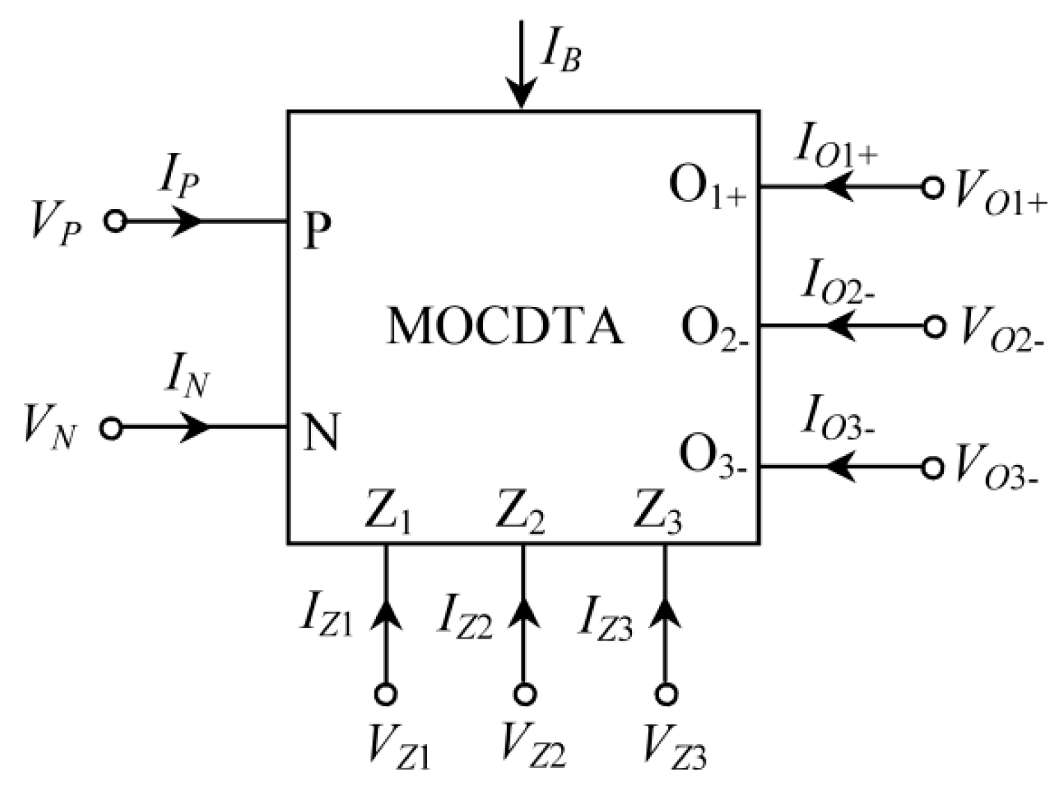
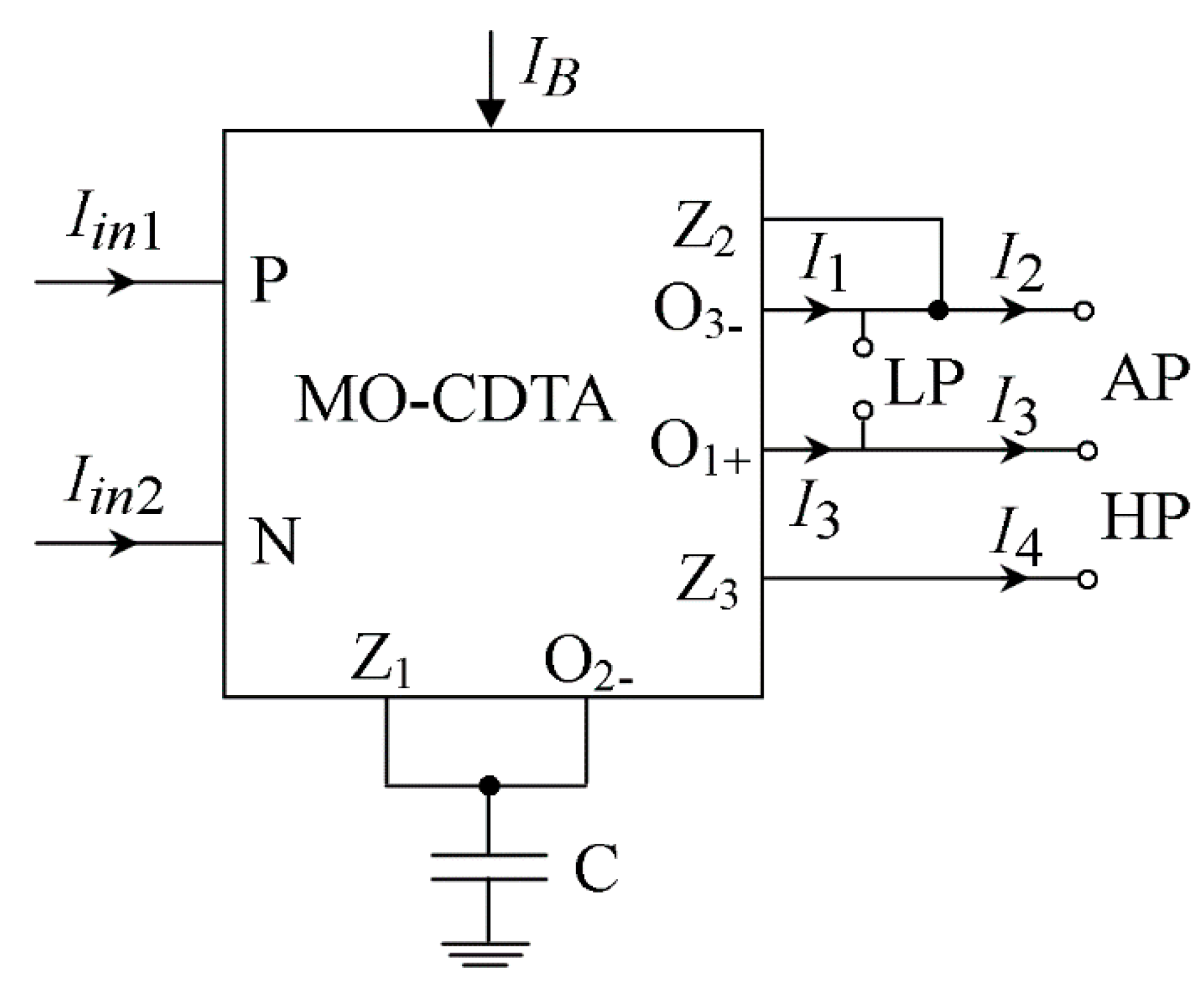
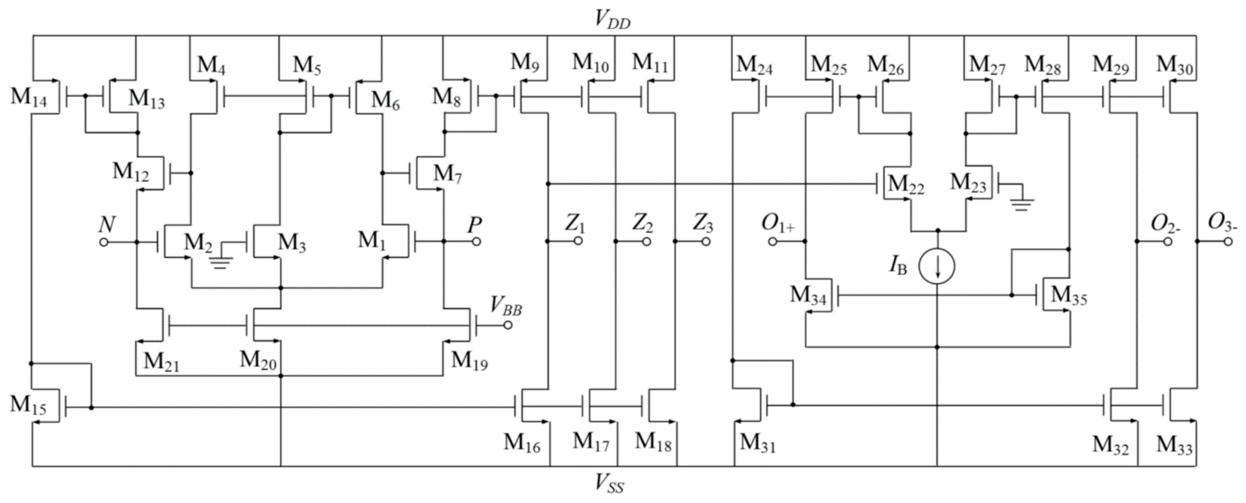
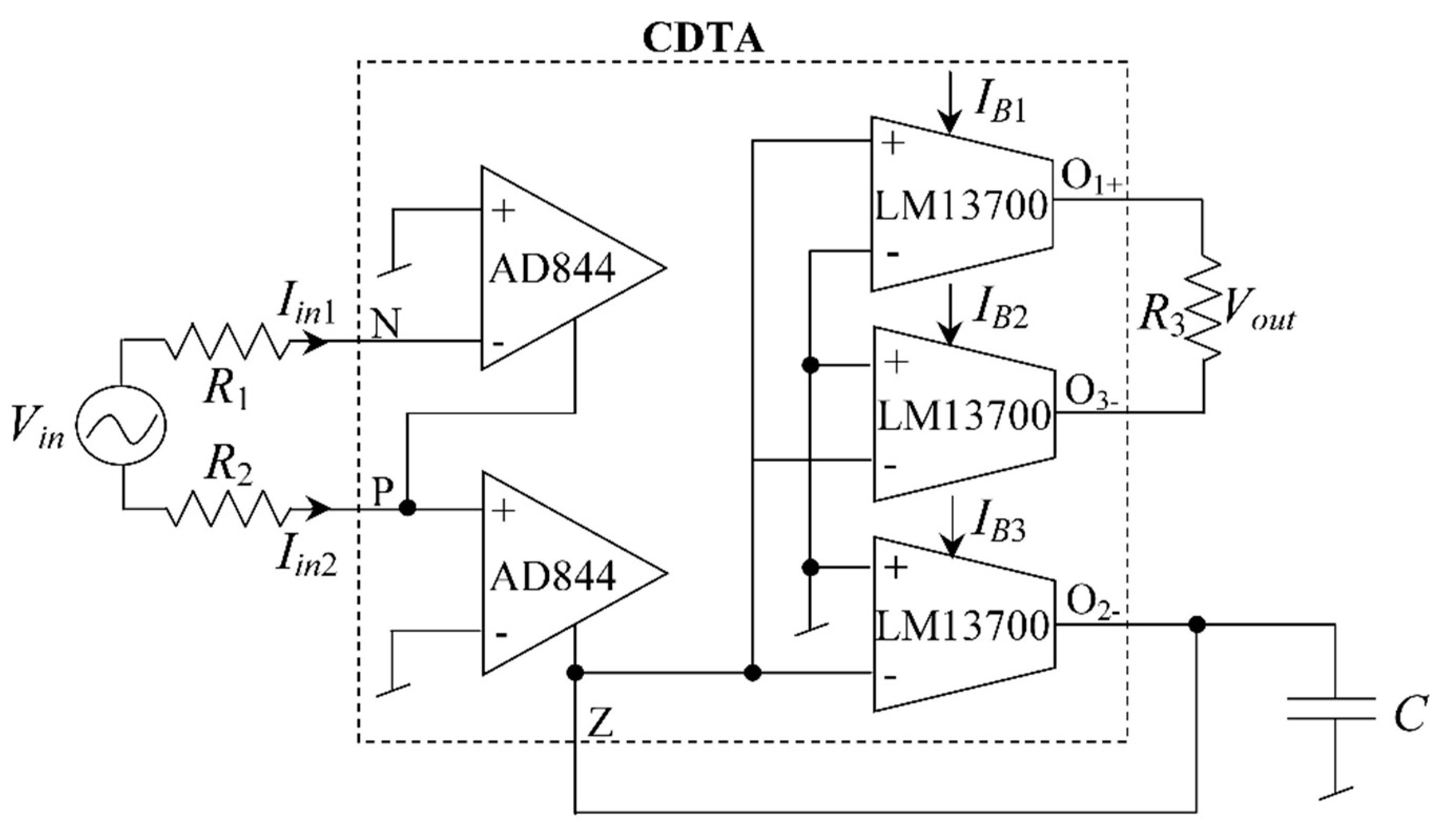
2. First-Order Fully Differential Configuration

The proposed first-order FD configuration is based on active element CDTA. The active element used, CDTA [21], is a versatile active element and has a wide operation frequency range. Numerous linear and non-linear circuits operating in voltage and/or current-mode, using CDTA, are presented in the literature [22,23,24,25]. A symbol of MOCDTA is depicted in Figure 1. The terminal relationships of MOCDTA are specified below.
[ I Z 1 I Z 2 I Z 3 I O 1 + I O 2 I O 3 ] = [ 1 1 0 0 0 1 1 0 0 0 1 1 0 0 0 0 0 g m 0 0 0 0 g m 0 0 0 0 g m 0 0 ] [ I P I N V Z 1 V Z 2 V Z 3 ]
where gm is transconductance gain of MOCDTA.
The proposed first-order FD configuration using single MOCDTA and one capacitor, which realizes LP, HP and AP filters within the same circuit structure, is shown in Figure 2. The input differential current (Iin = Iin1Iin2) signal is connected between low impedance terminals, whereas output differential current signals are accessible between high impedance terminals. Thus, the circuit offers rich cascadability without requiring any additional current buffer(s). By using the terminal relationships of Equation (1) and solving the nodal equations of the circuit, the following expressions of currents I1, I2, I3 and I4 are obtained.
I 1 = g m I i n s C + g m ,   I 2 = s C I i n s C + g m ,   I 3 = g m I i n s C + g m ,   I 4 = I i n
where I i n = I i n 1 I i n 2 .
The transfer functions of the proposed FD LP, HP and AP filters are given as follows:
I L P I i n = I 1 I 3 I i n 1 I i n 2 = 2 g m s C + g m
I H P I i n = I 3 I 4 I i n 1 I i n 2 = s C s C + g m
I A P I i n = I 2 I 3 I i n 1 I i n 2 = s C g m s C + g m
The pole frequency fP obtained from Equations (3)–(5) is given as follows:
f P = g m 2 π C
The pole frequency can be varied electronically by controlling the value of gm via the bias current of MOCDTA.

3. Non-Ideal and Parasitic Aspects

The non-ideal model of MOCDTA is specified below:
I Z 1 = α 1 ( I P I N ) , I Z 2 = α 2 ( I P I N ) , I Z 3 = α 3 ( I P I N ) , I O 1 + = γ 1 g m V Z 1 , I O 2 = γ 2 g m V Z 1 a n d I O 3 = γ 3 g m V Z 1
In Equation (7), α1, α2 and α3 are the non-ideal current transfer gains and γ1, γ2 and γ3 are the non-ideal transconductance gains. By considering the non-ideal model of Equation (7) and solving the nodal equations of the circuit, the following expressions of LP, HP and AP filter functions are obtained.
I L P I i n = α 1 ( γ 1 + γ 3 ) g m s C + γ 2 g m
I H P I i n = α 3 s C + g m ( α 3 γ 2 α 1 γ 1 ) s C + γ 2 g m
I A P I i n = α 2 s C + α 1 γ 1 g m + g m ( α 1 γ 3 α 2 γ 2 ) s C + γ 2 g m
Equations (8)–(10) show that the filter’s gain and pole frequency now depend upon the non-ideal gains. The new pole frequency obtained from Equations (8)–(10) is given as follows:
f P = γ 2 g m 2 π C
It is to be noted from Equation (11) that the pole frequency fP is not adversely affected and depends only on γ2, while it is independent of other non-idealities. It is to be mentioned that the −3 dB bandwidth of non-ideal gains is quite high, and at lower frequencies, their magnitude is almost the same. Therefore, the effects of these non-ideal gains at lower frequencies may be neglected. The sensitivities of fP relating to gm, capacitor and non-ideal gains are given in Equation (12), which conforms low-sensitivity figures.
S f P g m = S f P C = S f P γ 2 = 1 , S f P α 1 = S f P α 2 = S f P α 3 = S f P γ 1 = S f P γ 3 = 0
The following parasitic effects are included in MOCDTA: small resistances RP and RN in series at P and N terminals, respectively, and parallel combinations of RZ1//(1/sCZ1), RZ2//(1/sCZ2), RZ3//(1/sCZ3), RO1+//(1/sCO1+), RO2−//(1/sCO2−) and RO3−//(1/sCO3−) at Z1, Z2, Z3, O1+, O2−, and O3−, respectively. The inclusion of these parasitic effects may affect the proposed circuit, and reanalysis of the circuit gives the following expressions of transfer functions of the LP, HP and AP filters:
I L P I i n = 2 g m s C P + g m P
I H P I i n = s C P + 1 / R P s C P + g m P
I A P I i n = s C P g m P s C P + g m P
where g m P = g m + 1 R P , R P = R Z 1 + R O 2 and C P = C + C Z 1 + C O 2 .
The grounded capacitor C can easily absorb the parasitic capacitances CZ1 and CO2–. Equations (13)–(15) show that the proposed fully differential circuit is less affected by the parasitic effects of MOCDTA.
The pole frequency fP is now changed, as expressed below:
f P = g m P 2 π C P
The parasitic resistances RZ1 and RO2− are quite large in magnitude; therefore, gmPgm. Thus, the parasitic effects on pole frequency are negligible. The filter order is also not changed by the parasitic effects.

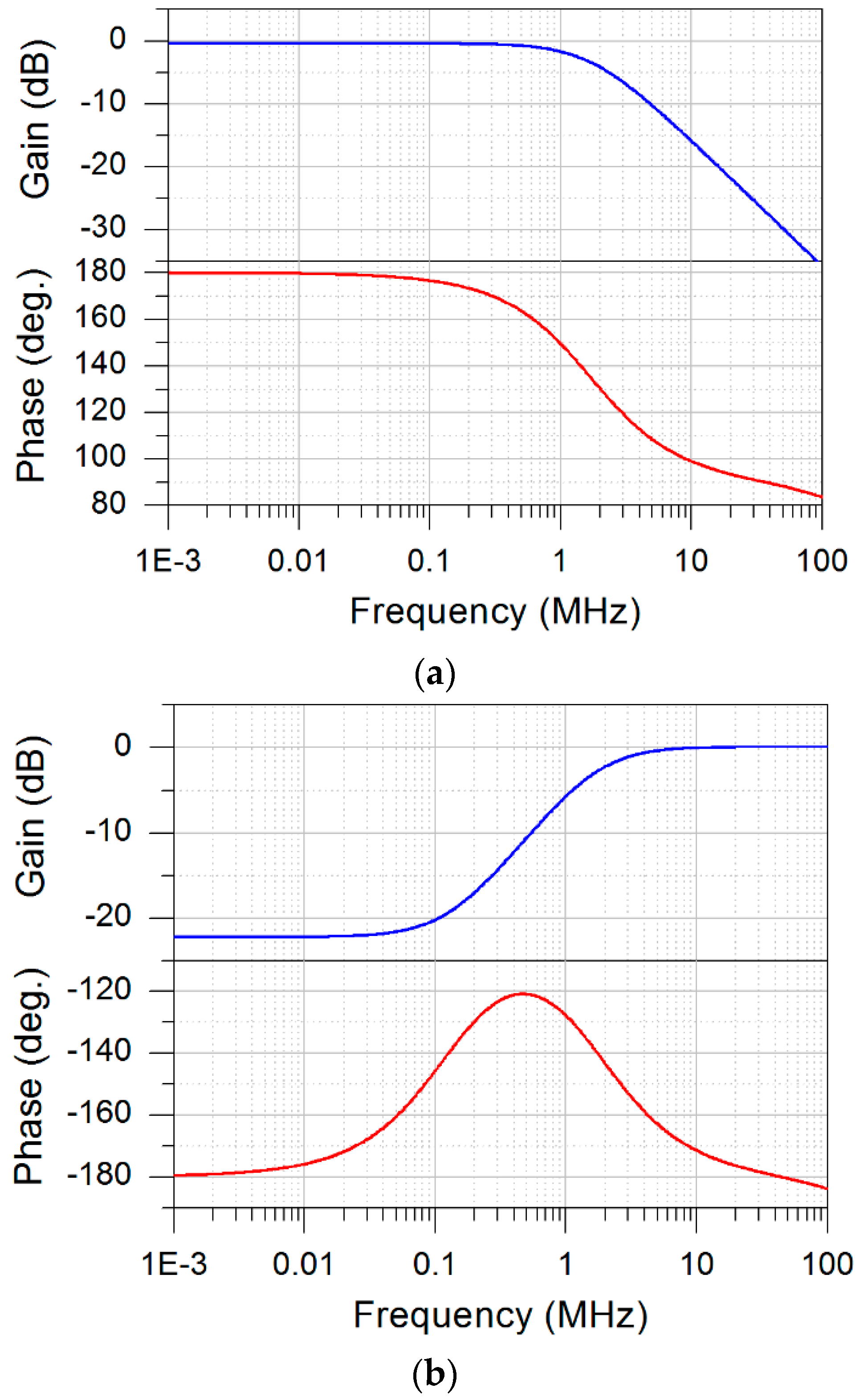
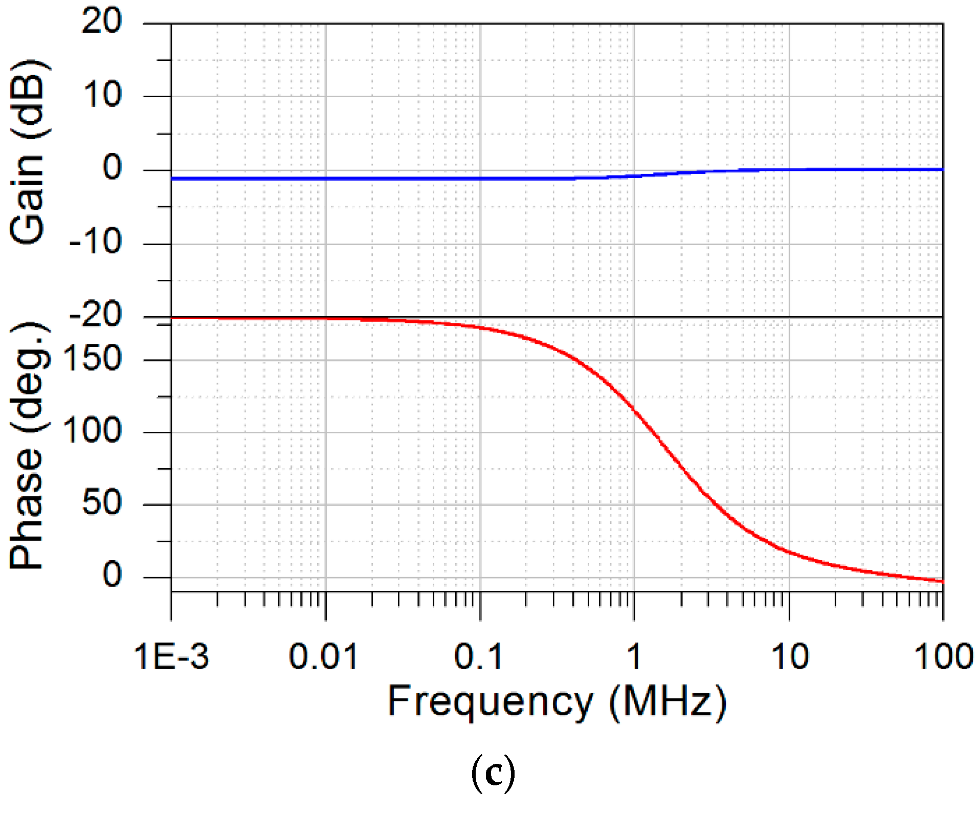
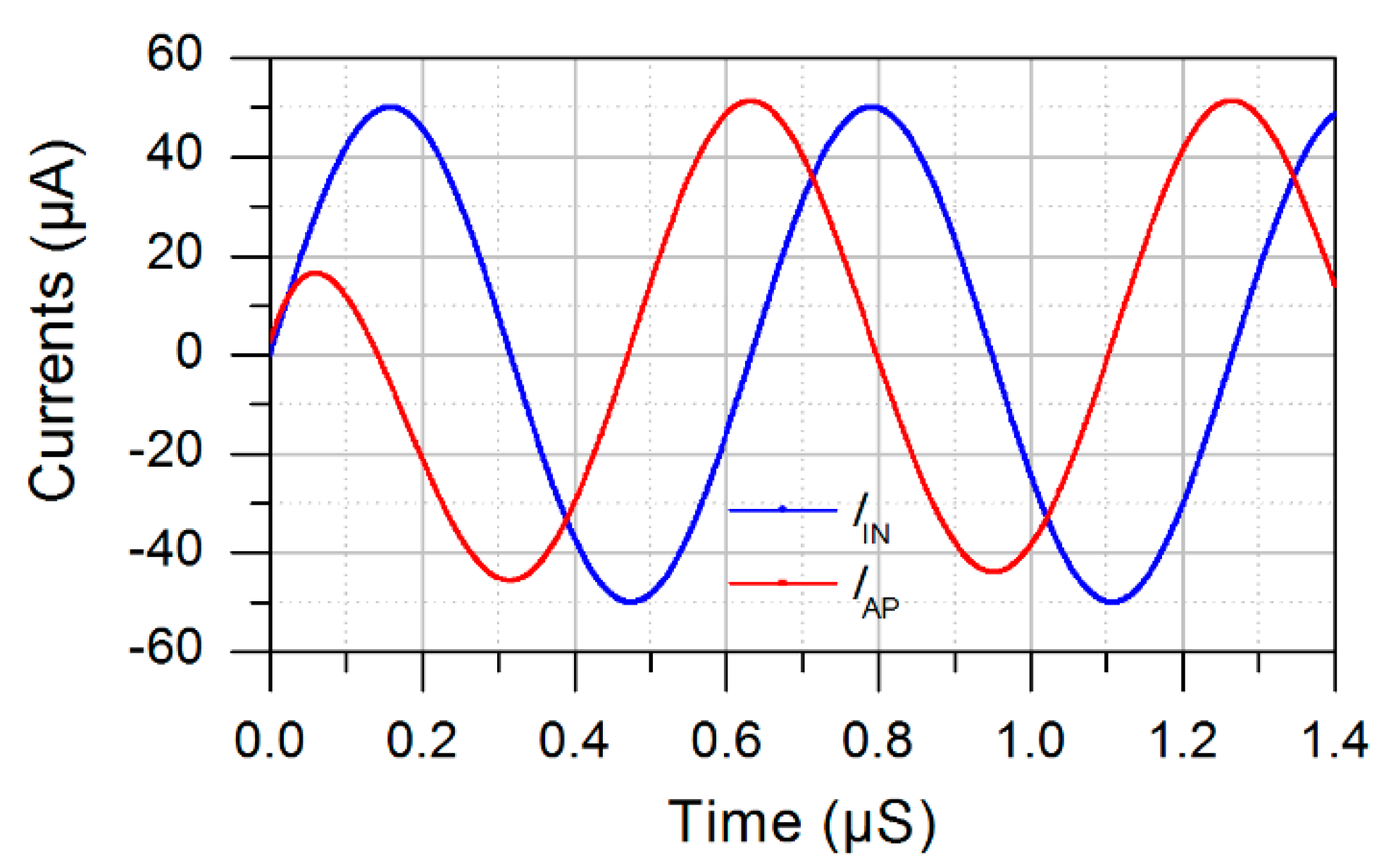
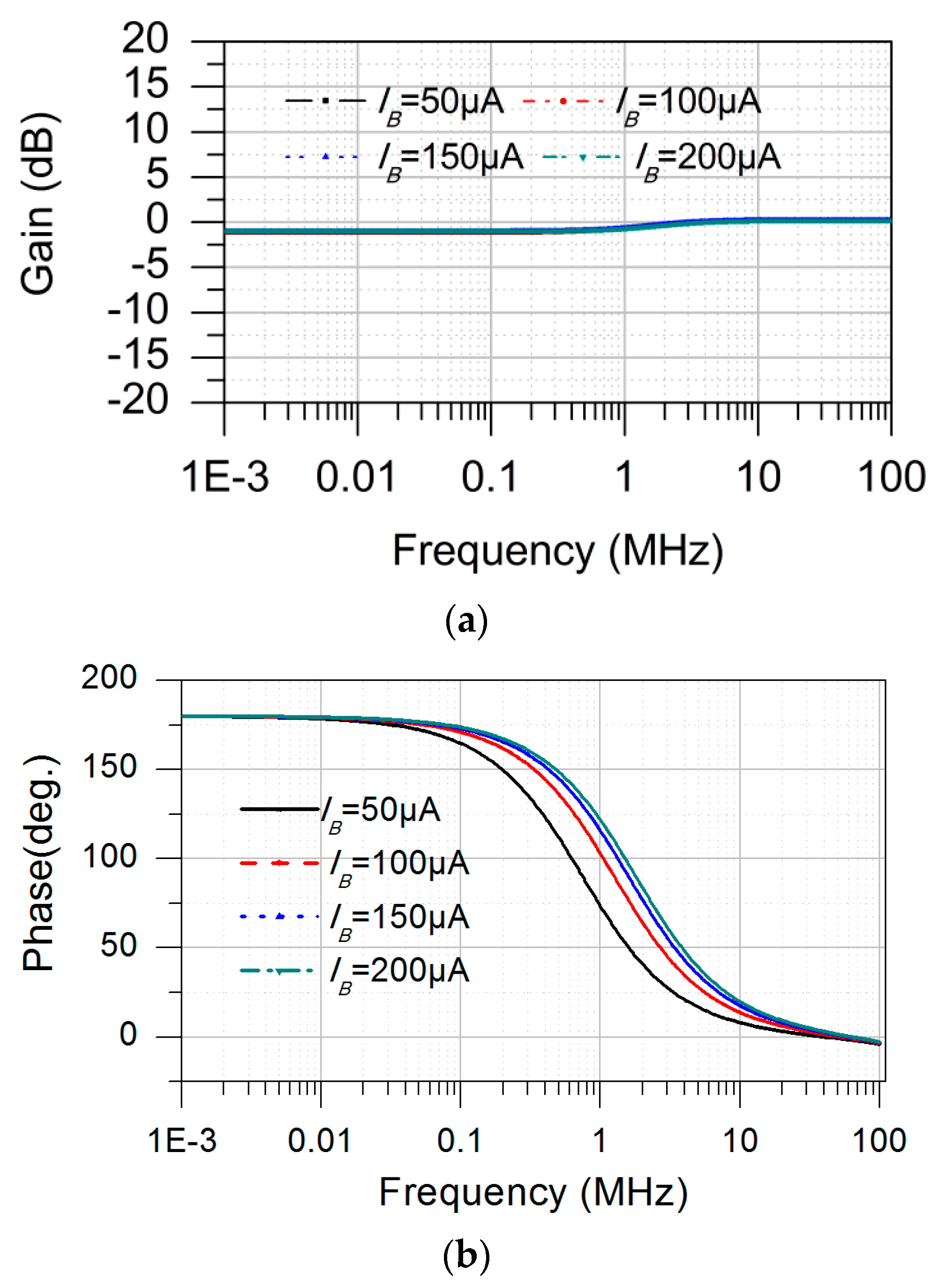
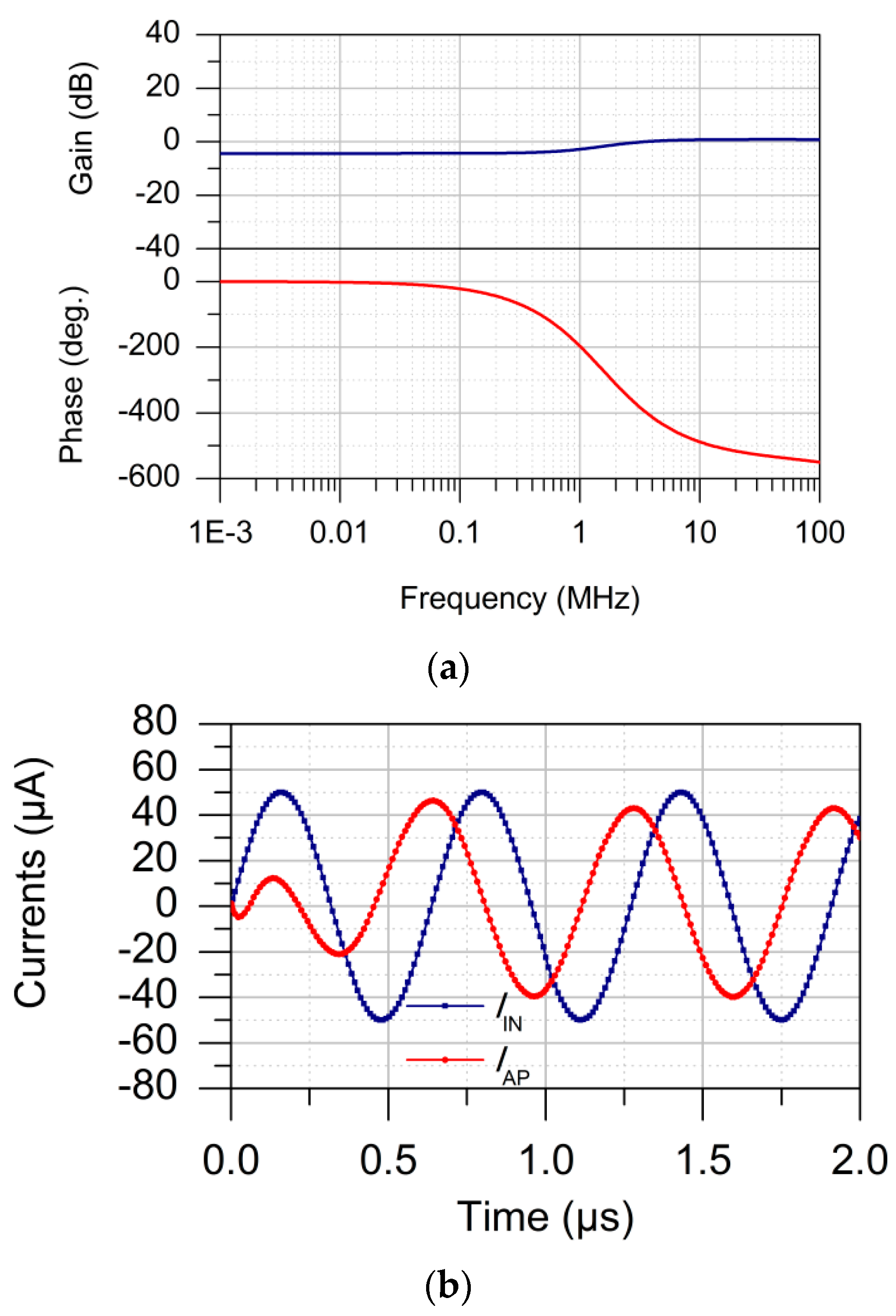
4. Simulation Results

The proposed FD first-order filters are simulated through PSPICE with 0.13 µm TSMC CMOS technology. The CMOS structure of MOCDTA is shown in Figure 3 [22] and the transistor’s W/L ratios are listed in Table 1. The supply voltage and bias voltage are set to ±1 V and −0.56 V, respectively. The bias current is IB = 150 µA (for which gm = 1 mS). The simulated values of non-idealities and parasitic effects of MOCDTA are given in Table 2. The designed pole frequency is 1.59 MHz, for which the capacitor is selected as 100 pF. The AC responses of the proposed circuit for gain and phase are shown in Figure 4. The simulated value of pole frequency is observed to be 1.587 MHz. The transient response for an AP filter at pole frequency, when a differential current of 50 µA in amplitude is applied at the input, is depicted in Figure 5. In Figure 5, the differential input and output current signals are in a quadrature relationship at pole frequency. The total harmonic distortion of AP output current is found to be less than 2%. The gain and phase plots of the AP filter for the bias current values of IB = 50, 100, 150 and 200 µA are depicted in Figure 6. The gain plots at different bias currents are overlapped with each other and phase plots at different values of bias current, IB = 50, 100, 150 and 200 µA, provide pole frequency values of 0.74, 1.24, 1.587 and 1.78 MHz, respectively. The high-frequency response of the circuit at 73 MHz is also tested for C = 2 pF and IB = 150 µA. The transient response for an AP filter at pole frequency of 73 MHz is depicted in Figure 7, which confirms the good operating frequency. Additionally, the temperature stability of the circuit is also examined. The transient responses for an AP filter for 0 °C to 75 °C temperature variations are depicted in Figure 8. It is noted that the performance of the circuit as a result of the temperature variation is not adversely deteriorated. Furthermore, Monte Carlo simulations for 1000 runs were carried out to verify the performance of the proposed circuit against capacitor variation and the MOS transistor’s threshold voltage variation. Figure 9 shows the histogram of maximum amplitude and pole frequency for an AP filter with 10% Gaussian deviation in capacitor values. Figure 10 shows the histogram of maximum amplitude and pole frequency for an AP filter with 5% Gaussian deviation in threshold voltages. For the capacitor deviation, the mean values of amplitude and pole frequency are 51.22 µA (2.44% error) and 1.58 MHz (0.62% error), respectively. For threshold voltage deviation, the mean values of amplitude and pole frequency are 51.37 µA (2.74% error) and 1.58 MHz (0.62% error), respectively. Figure 9 and Figure 10 confirm that the proposed FD circuit is less affected by the capacitor and threshold voltage variations. The proposed circuit consumes a maximum power (measured in simulation) of 2.5 mW at IB = 150 µA. Table 3 shows the key features of the proposed FD configuration, illustrating the advantages of the proposed first-order FD circuit over earlier reported first-order FD circuits.

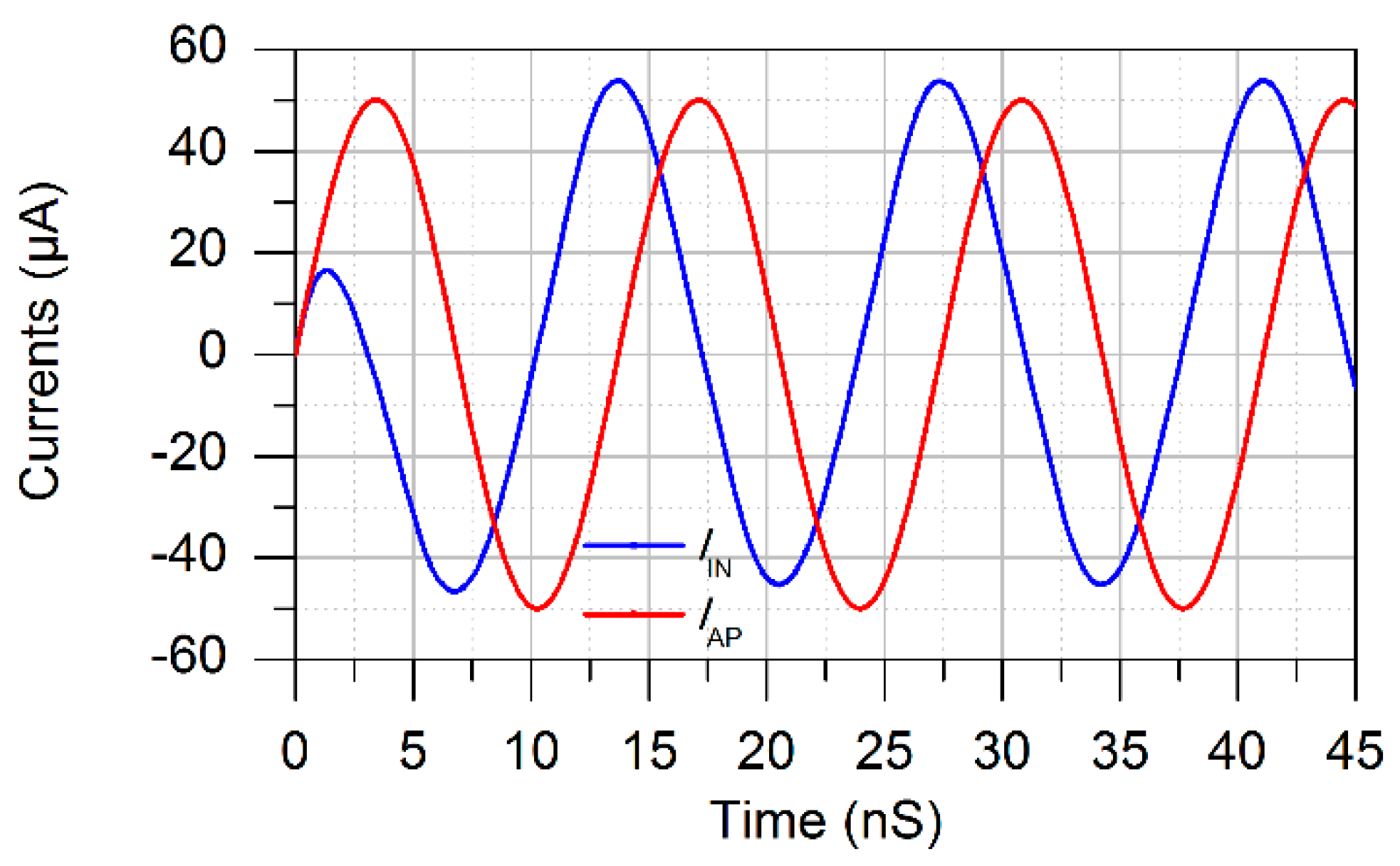
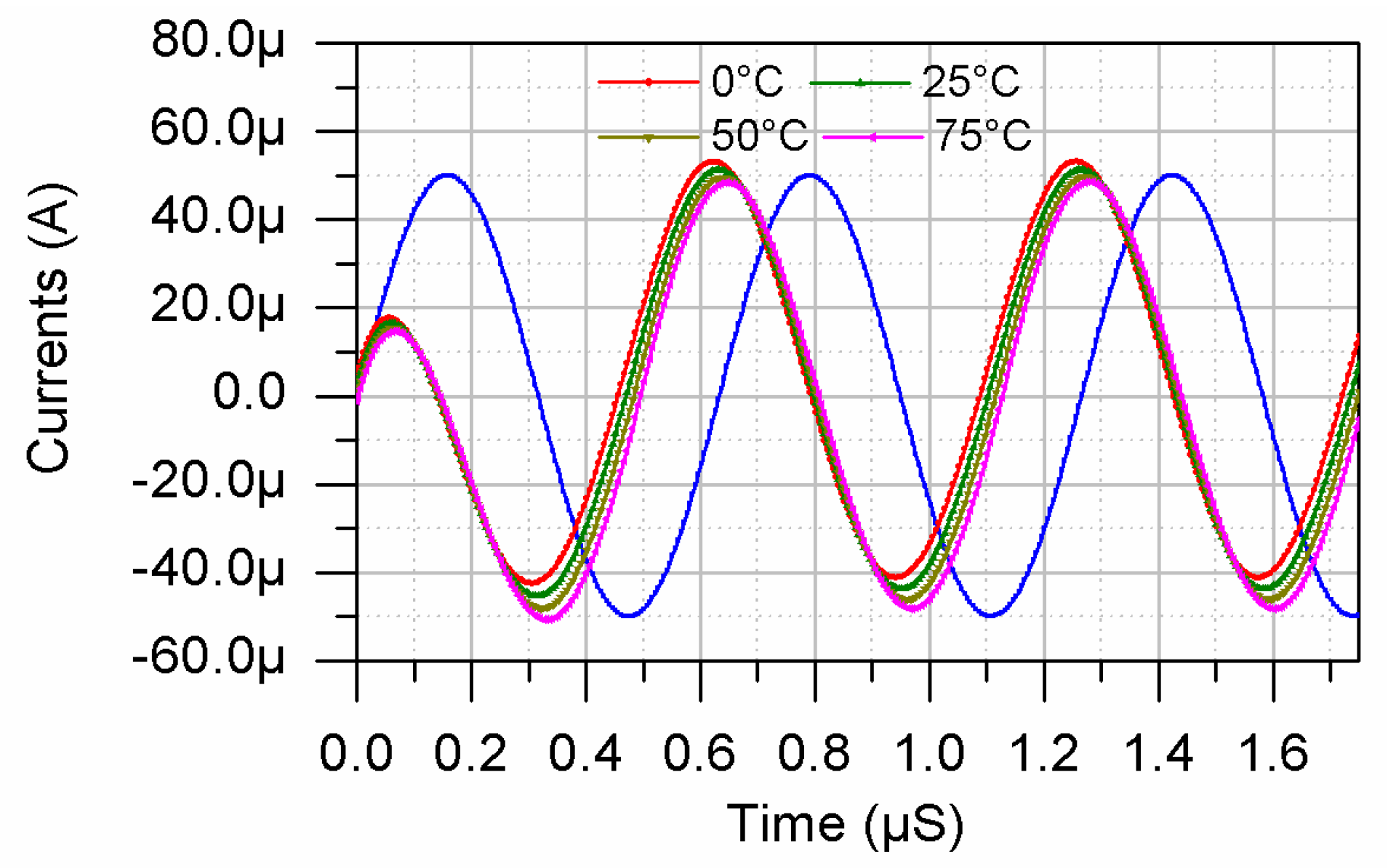
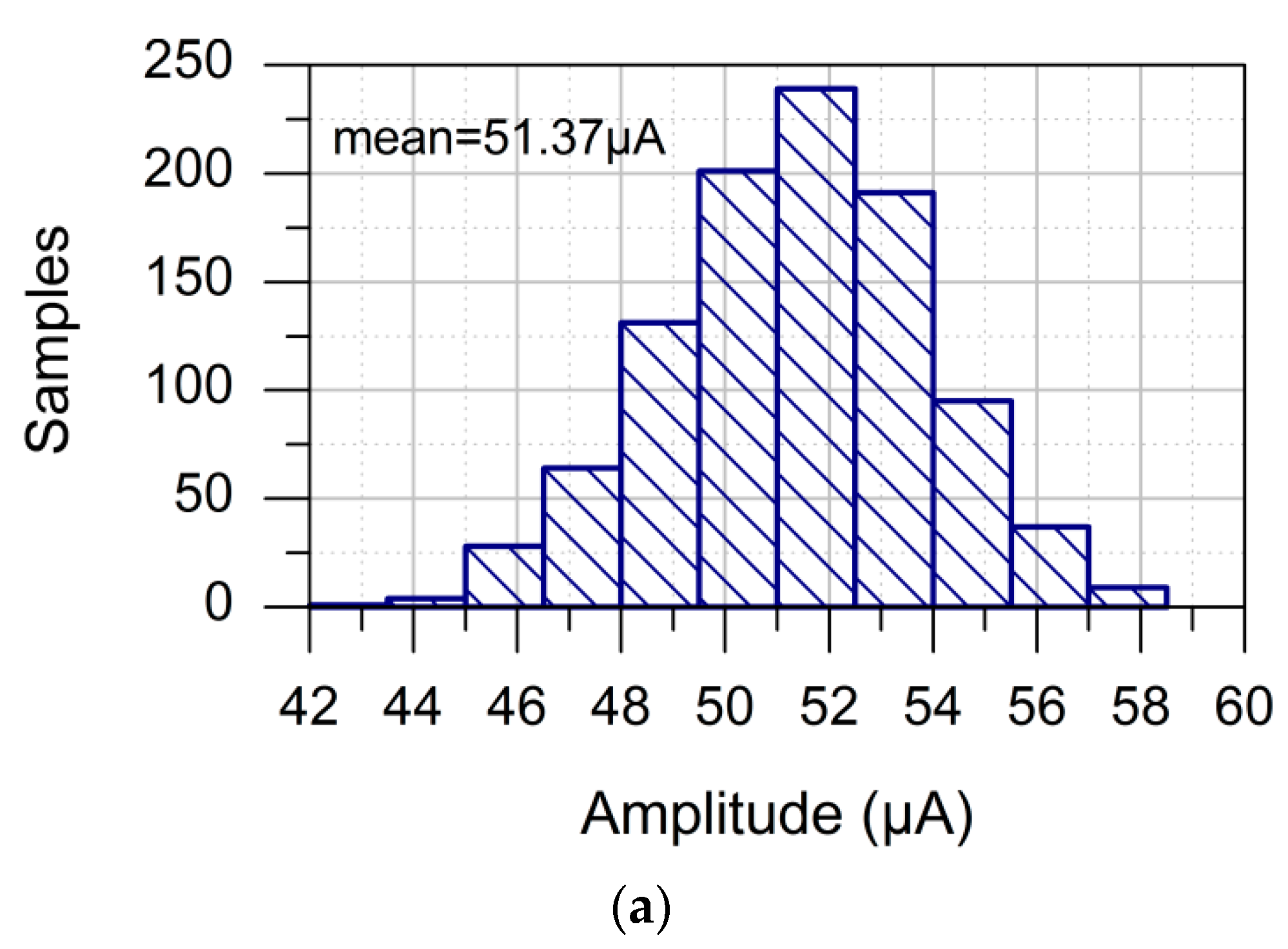
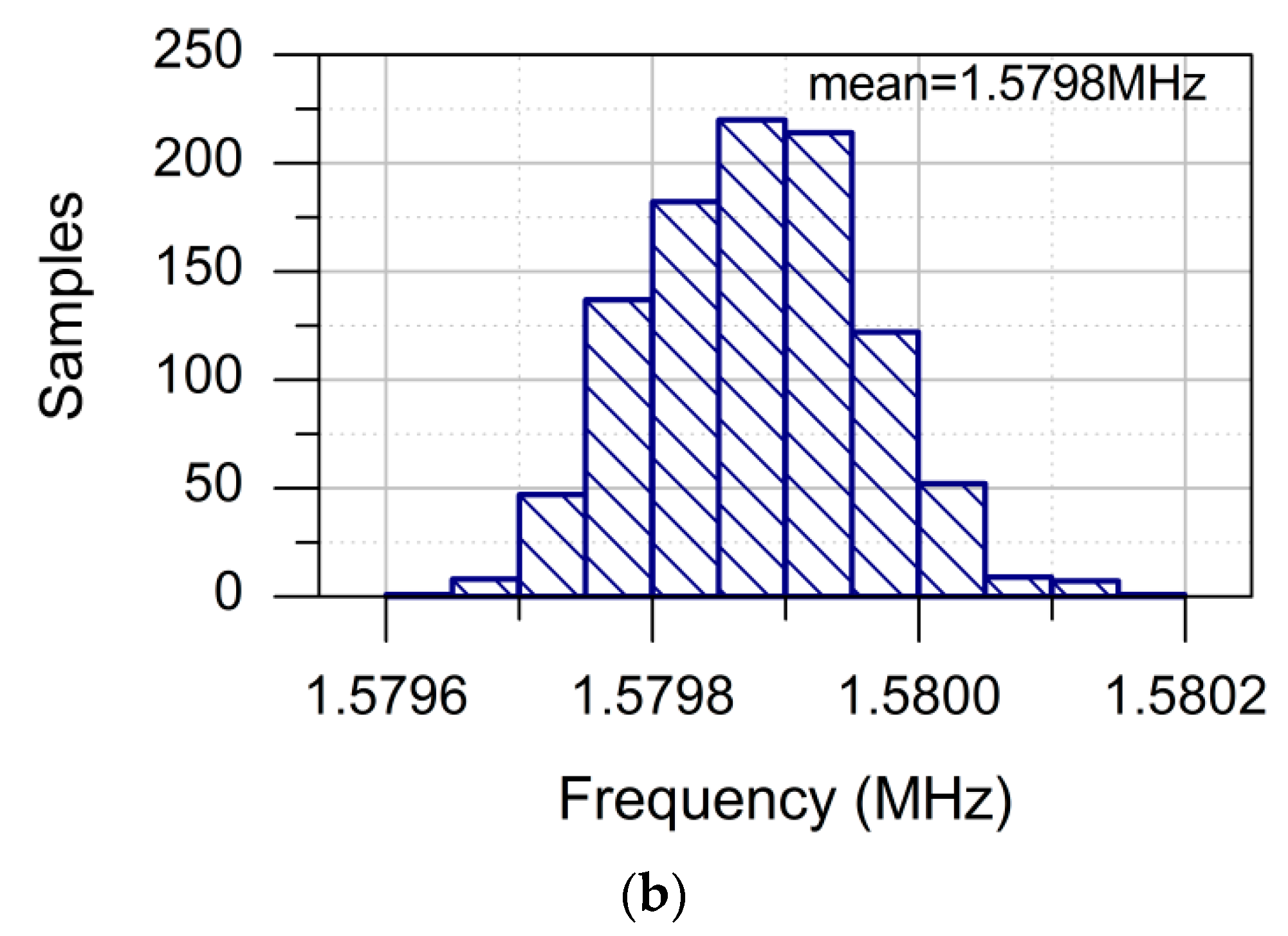
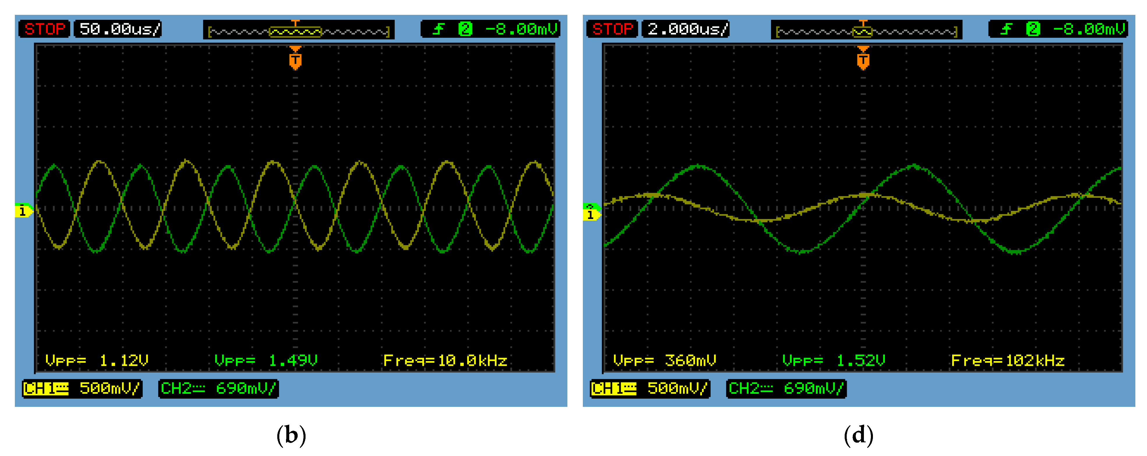
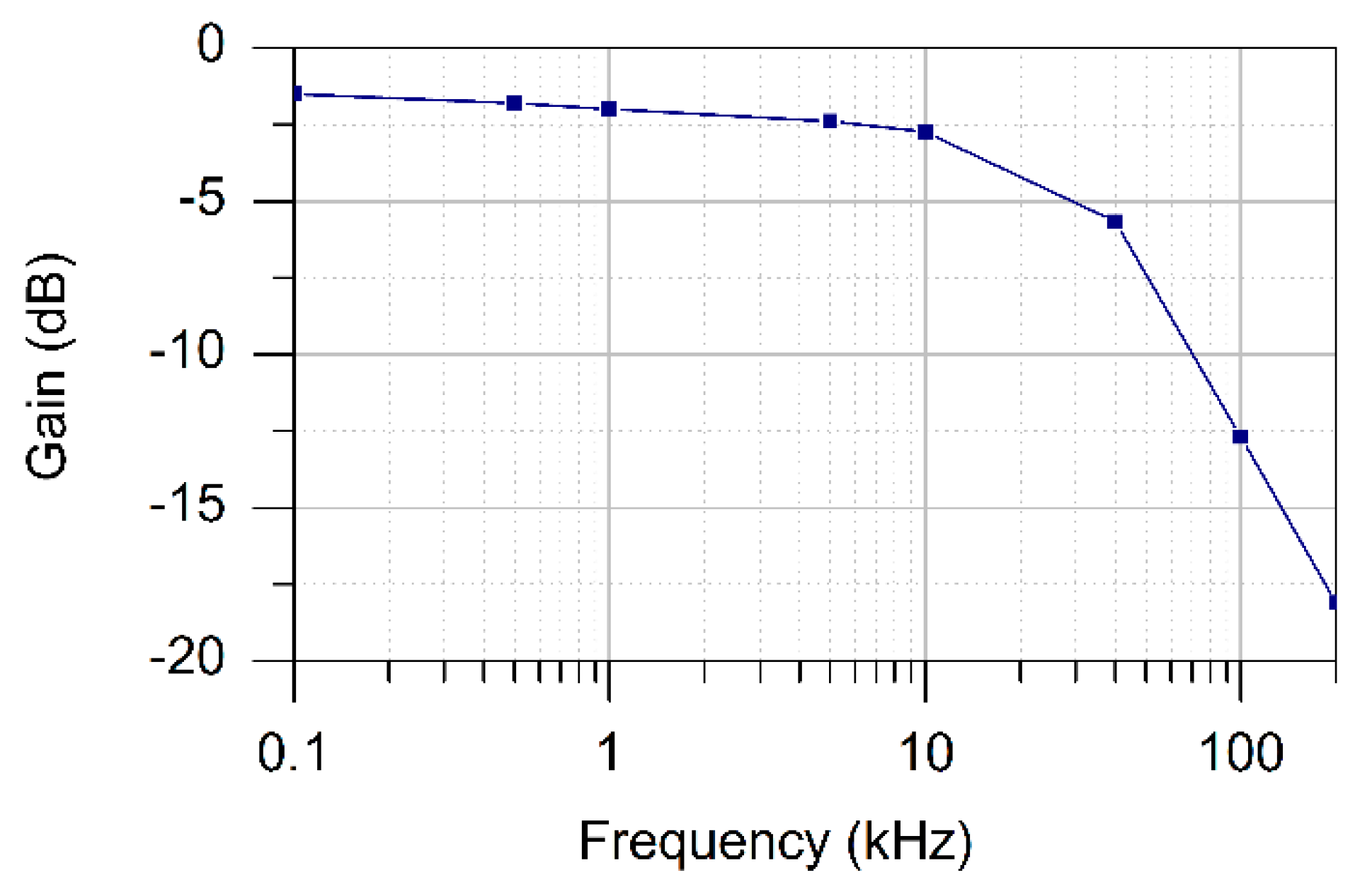
5. Experimental Results

The proposed fully differential LP filter configuration is experimentally verified using off-the-shelf ICs. The practical implementation of the proposed LP filter configuration is shown in Figure 11. The experimental set-up using breadboard and discrete components is depicted in Figure 12. The input currents Iin1 and Iin2 are applied with the help of external resistors R1 and R2, respectively. The output LP signal is observed across the load resistor R3. The power supplies used are ±10 V. The passive components are selected as follows: R1 = R2 = R3 = 1 kΩ, C = 10 nF. The bias current is set to 70 μA (gm = 1 mS). The input signal of 0.75 V in magnitude is applied to observe the output across resistor R3. Figure 13 shows the input and output signals at different frequencies (1 kHz, 10 kHz, 40 kHz and 100 kHz). A phase difference of 180° is clearly seen between the input and output at low frequency (1 kHz), which is in accordance with the simulation results shown in Figure 4a. Additionally, the plot of gain response for the LP filter configuration is shown in Figure 14.

6. Cascading Feasibility

The cascading ability of the presented configuration is further examined by realizing an nth-order FD LP filter. The output currents of the proposed fully differential filters are available from the high impedance terminals, making the proposed filters easily cascadable without requiring additional circuitry. Figure 15 shows the FD nth-order LP filter circuit, which is realized by cascading the n number of FD first-order LP filters. The transfer function of the realized FD nth-order LP filter is given as follows.
I L P I i n = I 1 I 2 I i n 1 I i n 2 = ( 2 g m s C + g m ) n
The pole frequency fP of the filter obtained from Equation (17) is given as follows:
f P = g m 2 π C
The nth-order circuit is validated by simulating it for n = 3. The circuit is simulated by using IB = 150 μA and C1 = C2 = C3 = 100 pF. The simulated gain and phase of the circuit are shown in Figure 16. The variation in the phase of the third-order LP filter from 0° to −270° is confirmed in Figure 16.
It should be noted that a higher-order HP filter and higher-order AP filter can also be implemented by cascading first-order filters in the same way as the higher-order LP filter shown in Figure 15. Figure 17 shows the gain and phase of the third-order HP filter. The frequency and transient responses of the third-order AP filter are shown in Figure 18. Figure 18a shows a phase variation of 0° to −540° for the AP filter.

7. Conclusions

In this paper, a MOCDTA-based FD first-order filter circuit, has been realized, with the LP, HP, and AP responses all obtainable within the same circuit structure. Low input and high output impedances are favorable for cascadability. Some other valuable features of the circuit include resistorless realization, use of grounded capacitor only, electronic tunability, lower sensitivity figures, low operating supply voltages, wider operational frequency range and low power consumption. The proposed FD configuration is less affected by temperature variation, capacitor variation and threshold voltage variation. An nth-order FD LP filter has also been realized to demonstrate the cascading feasibility of the proposed FD first-order filter. The fully differential operability of the proposed circuit makes it favorable for several applications, such as audio systems, data transmission and communication systems.

Author Contributions

Conceptualization, A.K. and S.K.; methodology, A.K.; software, A.K.; validation, S.U. and D.H.E.; formal analysis, S.K.; resources, S.U. and D.H.E.; writing—original draft preparation, A.K. and S.K.; writing—review and editing, S.U. and D.H.E.; supervision, S.K.; project administration, S.K.; funding acquisition, S.U. and D.H.E. All authors have read and agreed to the published version of the manuscript.

Funding

This research is funded by Princess Nourah bint Abdulrahman University Researchers Supporting Project number (PNURSP2022R238), Princess Nourah bint Abdulrahman University, Riyadh, Saudi Arabia.

Institutional Review Board Statement

Not applicable.

Informed Consent Statement

Not applicable.

Data Availability Statement

Not applicable.

Acknowledgments

Princess Nourah bint Abdulrahman University Researchers Supporting Project number (PNURSP2022R238), Princess Nourah bint Abdulrahman University, Riyadh, Saudi Arabia.

Conflicts of Interest

The authors declare no conflict of interest.

References

  1. Senani, R.; Bhaskar, D.R.; Kumar, P. Two-CFOA-grounded-capacitor first-order all-pass filter configurations with ideally infinite input impedance. AEU-Int. J. Electron. Commun. 2021, 137, 153742. [Google Scholar] [CrossRef]
  2. Chaturvedi, B.; Kumar, A. Realization of novel cascadable current-mode all-pass sections. Iran. J. Electr. Electron. Eng. 2018, 14, 162–169. [Google Scholar]
  3. Yucel, F. A DVCC-Based Current-Mode First-Order Universal Filter. J. Circuits Syst. Comput. 2021, 30, 2150305. [Google Scholar] [CrossRef]
  4. Maheshwari, S. Tuning approach for first-order filters and new current-mode circuit example. IET Circuits Devices Syst. 2018, 12, 478–485. [Google Scholar] [CrossRef]
  5. Chaturvedi, B.; Kumar, A. Electronically tunable first-order filters and dual-mode multiphase oscillator. Circuits Syst. Signal Process. 2019, 38, 2–5. [Google Scholar] [CrossRef]
  6. Tarunkumar, H.; Ranjan, A.; Pheiroijam, N.M. First Order and Second Order Universal Filter Using Four Terminal Floating Nullor. Int. J. Eng. Technol. 2018, 7, 192–198. [Google Scholar]
  7. Chaturvedi, B.; Kumar, A.; Mohan, J. Low voltage operated current-mode first-order universal filter and sinusoidal oscillator suitable for signal processing applications. AEU-Int. J. Electron. Commun. 2019, 99, 110–118. [Google Scholar] [CrossRef]
  8. Herencsar, N.; Koton, J.; Hanak, P. Universal voltage conveyor and its novel dual-output fully-cascadable VM APF application. Appl. Sci. 2017, 7, 307. [Google Scholar] [CrossRef]
  9. Barile, G.; Safari, L.; Pantoli, L.; Stornelli, V.; Ferri, G. Electronically tunable first order AP/LP and LP/HP filter topologies using electronically controllable second generation voltage conveyor (CVCII). Electronics 2021, 10, 822. [Google Scholar] [CrossRef]
  10. Jaikla, W.; Buakhong, U.; Siripongdee, S.; Khateb, F.; Sotner, R.; Silapan, P.; Suwanjan, P.; Chaichana, A. Single Commercially Available IC-Based Electronically Controllable Voltage-Mode First-Order Multifunction Filter with Complete Standard Functions and Low Output Impedance. Sensors 2021, 21, 7376. [Google Scholar] [CrossRef] [PubMed]
  11. Dogan, M.; Yuce, E. A first-order universal filter including a grounded capacitor and two CFOAs. Analog Integr. Circuits Signal Process. 2022, 26, 1–2. [Google Scholar] [CrossRef]
  12. Phatsornsiri, P.; Kumngern, M.; Khateb, F. 0.5-V fully differential allpass section. In Proceedings of the 2016 International Symposium on Intelligent Signal Processing and Communication Systems (ISPACS), Phuket, Thailand, 24–27 October 2016; IEEE: Piscataway, NJ, USA, 2016; pp. 1–4. [Google Scholar]
  13. Maheshwari, S.; Chaturvedi, B.; Tiwari, P.K.; Khan, I.A. Fully differential first order all-pass filter circuit. In Proceedings of the National Conference on Modern Trends in Electronic and Communication Systems (MTECS), Aligarh, India, 8–9 March 2008; pp. 131–134. [Google Scholar]
  14. Horng, J.W.; Wu, C.M.; Herencsar, N. Fully differential first-order allpass filters using a DDCC. Indian J. Eng. Mater. Sci. 2014, 21, 345–350. [Google Scholar]
  15. Khan, I.A.; Masud, M.I.; Moiz, S.A. Reconfigurable fully differential first order all pass filter using digitally controlled CMOS DVCC. In Proceedings of the 2015 IEEE 8th GCC Conference & Exhibition, Muscat, Oman, 1–4 February 2015; pp. 1–5. [Google Scholar]
  16. Beg, P.; Ansari, M.S. Fully-differential first-order all-pass filters using CMOS DV-DXCCII. In Proceedings of the 2017 International Conference on Multimedia, Signal Processing and Communication Technologies (IMPACT), Aligarh, India, 24–26 November 2017; pp. 267–270. [Google Scholar]
  17. Ansari, M.S.; Soni, G.S. Digitally-programmable fully-differential current-mode first-order LP, HP and AP filter sections. In Proceedings of the 2014 International Conference on Signal Propagation and Computer Technology (ICSPCT 2014), Ajmer, India, 12–13 July 2014; pp. 524–528. [Google Scholar]
  18. Herencsar, N.; Jerabek, J.; Koton, J.; Vrba, K.; Minaei, S.; Göknar, İ.C. Pole frequency and pass-band gain tunable novel fully-differential current-mode all-pass filter. In Proceedings of the 2015 IEEE International Symposium on Circuits and Systems (ISCAS), Lisbon, Portugal, 24–27 May 2015; pp. 2668–2671. [Google Scholar]
  19. Kumngern, M.; Khateb, F.; Kulej, T. Bulk-driven fully balanced second-generation current conveyor in 0.18 µm CMOS. AEU-Int. J. Electron. Commun. 2019, 104, 66–75. [Google Scholar] [CrossRef]
  20. İbrahim, M.A.; Minaei, S.; Kuntman, H. DVCC based differential-mode all-pass and notch filters with high CMRR. Int. J. Electron. 2006, 93, 231–240. [Google Scholar] [CrossRef]
  21. Biolek, D. CDTA-building block for current-mode analog signal processing. In Proceedings of the ECCTD’03, Krakow, Poland, 1–4 September 2003; Volume III, pp. 397–400. [Google Scholar]
  22. Keskin, A.Ü.; Biolek, D.; Hancioglu, E.; Biolková, V. Current-mode KHN filter employing current differencing transconductance amplifiers. AEU-Int. J. Electron. Commun. 2006, 60, 443–446. [Google Scholar] [CrossRef]
  23. Keskin, A.Ü.; Biolek, D. Current mode quadrature oscillator using current differencing transconductance amplifiers (CDTA). IEE Proc.-Circuits Devices Syst. 2006, 153, 214–218. [Google Scholar] [CrossRef] [Green Version]
  24. Biolek, D.; Hancioglu, E.; Keskin, A.Ü. High-performance current differencing transconductance amplifier and its application in precision current-mode rectification. AEU-Int. J. Electron. Commun. 2008, 62, 92–96. [Google Scholar] [CrossRef] [Green Version]
  25. Khateb, F.; Vavra, J.; Biolek, D. A Novel Current-Mode Full-Wave Rectifier Based on One CDTA and Two Diodes. Radioengineering 2010, 19, 437–445. [Google Scholar]
Figure 1. Symbol of MOCDTA.
Electronics 11 02072 g001
Figure 2. The proposed fully differential configuration realizing first-order filters.
Electronics 11 02072 g002
Figure 3. CMOS implementation of MOCDTA.
Electronics 11 02072 g003
Figure 4. Frequency responses of gain and phase: (a) LP; (b) HP; (c) AP.
Electronics 11 02072 g004aElectronics 11 02072 g004b
Figure 5. Differential input current and differential AP output current at 1.58 MHz.
Electronics 11 02072 g005
Figure 6. Frequency responses of AP filter at different bias current for (a) gain and (b) phase.
Electronics 11 02072 g006
Figure 7. Differential input current and differential AP output current at 73 MHz.
Electronics 11 02072 g007
Figure 8. Transient responses of differential AP output currents at 0, 25, 50 and 75 °C.
Electronics 11 02072 g008
Figure 9. Monte Carlo simulation results for the variation in capacitor value: (a) histogram for maximum amplitude; (b) histogram for pole frequency.
Electronics 11 02072 g009
Figure 10. Monte Carlo simulation results for the variation in threshold voltages: (a) histogram for maximum amplitude; (b) histogram for pole frequency.
Electronics 11 02072 g010aElectronics 11 02072 g010b
Figure 11. Practical implementation of the proposed fully differential LP filter.
Electronics 11 02072 g011
Figure 12. Experimental set-up using breadboard and discrete components.
Electronics 11 02072 g012
Figure 13. Experimental results of the LP filter showing input and output waveforms at (a) 1 kHz, (b) 10 kHz, (c) 40 kHz and (d) 100 kHz.
Electronics 11 02072 g013aElectronics 11 02072 g013b
Figure 14. Plot of gain response for the LP filter for experimental results.
Electronics 11 02072 g014
Figure 15. The proposed fully differential configuration realizing the nth-order LP filter.
Electronics 11 02072 g015
Figure 16. Frequency responses of gain and phase of the third-order LP filter.
Electronics 11 02072 g016
Figure 17. Frequency responses for gain and phase of the third-order HP filter.
Electronics 11 02072 g017
Figure 18. Third-order AP filter’s responses: (a) frequency responses of gain and phase; (b) transient response for differential input and output currents.
Electronics 11 02072 g018
Table 1. W/L ratios of MOS transistors.
MOS TransistorsW(μm)/L(μm) Ratio
M1–M326/0.26
M4–M6,10.4/0.26
M8–M11, M13–M18, M22, M233.9/0.26
M7, M1215.6/0.26
M19–M2113/0.26
M24–M301.5/0.26
M31–M351/0.26
Table 2. Simulated values of non-idealities and parasitic effects of MOCDTA.
ParameterSimulated Value
α1, α2, α30.99
−3 dB bandwidth of α1, α2, α31 GHz
−3 dB bandwidth of γ1, γ2, γ32 GHz
RP, RN14 Ω
RZ1, RZ2100 kΩ
RO1+, RO2−, RO3−125 kΩ
Table 3. Comparison among the proposed fully differential first-order circuit and earlier reported fully differential first-order circuits.
Ref.Active Element/
Count
Passive Components with CountAll Grounded Passive ComponentPassive Component Matching RestrictionOperating ModeCascadableAvailability of LP, HP and AP ResponsesMOS Transistors CountTechnology (µm)Max Operation FrequencySupply Voltage(s) (V)
[12]FDDTA/11-R, 2-CNoYesVMNoOnly AP340.180.04 MHz0.5
[13]DVCC/13-R, 1-CNoYesVMNoOnly AP180.52.27 MHz±2.5
[14]DDCC/13-R, 1-CNoYesVMNoOnly AP120.180.32 MHz±0.9
[15]DPDVCC/22-R, 2-CNoYesVMNoAP and LP or AP and HP920.250.27 MHz±2.5
[16]DV-DXCCII/13-R, 2-C or 2-R, 3-CNoYesVMNoOnly AP300.256.13 MHz±1.25
[17]DC-DVCC/12-R, 1-CNoYesCMYesLP and HP380.51.58 MHz±2.5
DC-DVCC/24-R, 2-CNoYesCMYesOnly AP760.51.58 MHz±2.5
[18]ACA/1, CF/21-CNoNoCMYesOnly AP500.180.94 MHz±1.2
[19]FBCCII/16-R, 2-CNoYesVMNoOnly AP340.18290 Hz0.5
[20]DVCC/11-R, 3-CNoYesVMNoOnly AP180.53.18 MHz±2.5
This workMOCDTA/11-CYesNoCMYesAll LP, HP and AP350.1373 MHz±1
FDDTA: fully differential difference transconductance amplifier, DVCC: differential voltage current conveyor, DDCC: differential difference current conveyor, DPDVCC: digitally programmable DVCC, DV-DXCCII: differential voltage dual-X second-generation current conveyor, DC-DVCC: digitally controllable DVCC, ACA: adjustable current amplifier, CF: current follower, FBCCII: fully balanced CCII, VM: voltage mode, CM: current mode, LP: low-pass, HP: high-pass, AP: all-pass.
Publisher’s Note: MDPI stays neutral with regard to jurisdictional claims in published maps and institutional affiliations.

