Abstract
We present a high-stability regulation circuit to ensure the safety of a device within a wide range of the back-sink current for a USB Type-C interface application. The proposed adaptive linear pole–zero tracking compensation can linearly compensate for the changes in the back-sink current, thereby adaptively canceling the pole–zero changes caused by the current changes. The simulation results show that the phase margin remains greater than 60°. Meanwhile, the loop bandwidth changes between 45 kHz and 135 kHz, when the current increases from 0 A to 1 A, ensuring excellent loop stability. The high-stability regulation circuit is realized in a standard 180 nm CMOS process with an area of 0.4 mm × 0.6 mm. The chip regulates an output voltage from 4.5 V to 5.5 V with 1 A current capacity and 100 mV maximum dropout voltage with the help of the adaptive linear pole–zero tracking compensation.
1. Introduction
The USB Type-C interface is significantly advantageous over the conventional data transmission interfaces and has been widely used in various portable electronic devices such as notebooks, desktops and smartphones [1]. The current-limiting switch between the Type-C interface and peripherals is employed to prevent overcurrent, short-circuit or even reverse-current, thus effectively protecting the safety of the host and the device.
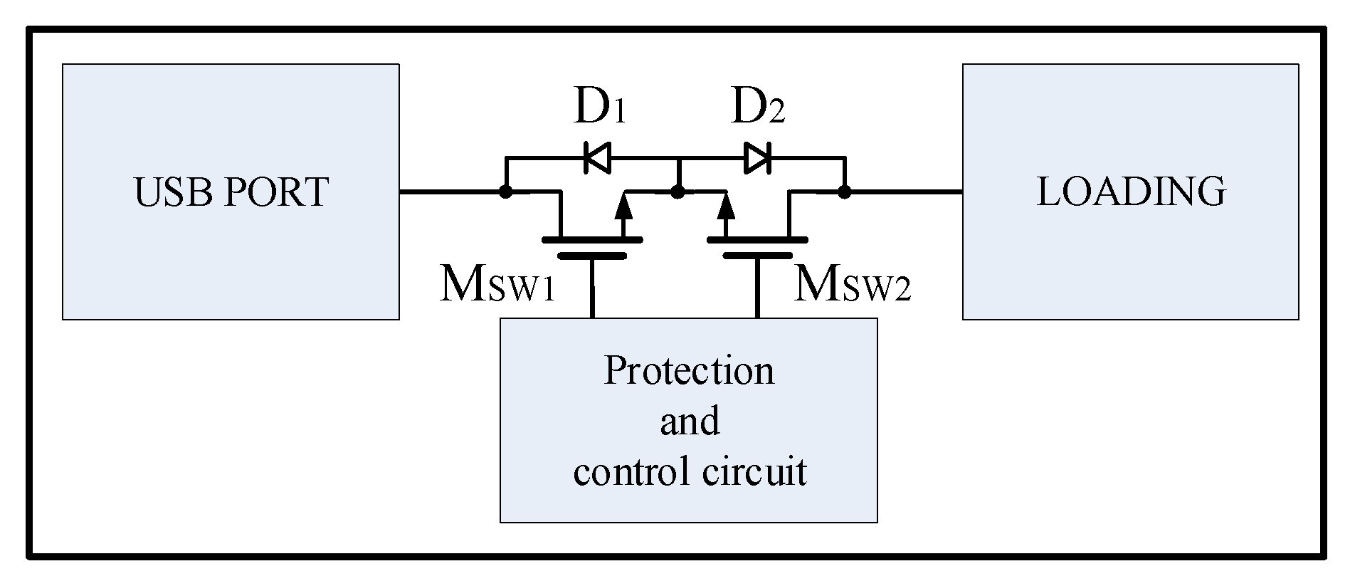
Figure 1 shows the schematic structure of a typical USB interface protection circuit. Two NMOS switches MSW1 and MSW2 are connected in series, and the substrate can be prevented from being turned on when the switch is turned off. In practice, MSW1 is used for the current limit protection while MSW2 is employed to protect against the reverse current. The voltage stabilization loop used to control MSW2 is similar to the LDO structure, but the difference from the traditional LDO is that the dropout voltage of the loop needs to be reduced (<100 mV) to avoid the power loss of the switch itself [2,3,4,5,6,7,8,9,10,11]. Under such a low dropout voltage, the working state of the MSW2 transistor is approximately in the linear region. It should be noted that according to the protocol requirements of USB3.X, the current flowing through the switch varies from 0 A to several amperes corresponding to the change of the load on the output terminal of the switch, which poses difficulties for the compensation of the loop stability [1].
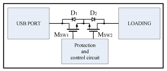
Figure 1.
Schematic diagram of the USB interface protecting circuit.
Due to the large capacitance (microfarad-level) connected to the switch output as the stabilized capacitor for power supply measurement, the output pole appears at a very low frequency when the load current is small. A large capacitance is thus required for conventional Miller compensation, which, however, is unacceptable for a chip application with limited floor space. On the other hand, the traditional equivalent series resistor (ESR) compensation has the problem of zero drift with limited compensation stability [2]. Dynamic pole–zero tracking frequency compensation can compensate the first nondominant pole in multistage op-amps by dynamically generating zeros [3,4]. However, in the conventional pole–zero compensation method, although the tracking MOS transistor works in the saturation region, the zero resistance works in the linear region leading to a continuous change in the impedance, which can further result in a large variation in the relative position of the pole–zero in the full current range. This can have a significant influence on the variation range of the bandwidth, making it unsuitable for the application of a current limiting switch system. In this work, an adaptive linear pole–zero tracking compensation method is proposed by introducing a current detection loop and a constant bandwidth tracking loop. While the loop stability is not affected by the change of the load current, the gain bandwidth of the entire loop is constant at a certain level.
2. Traditional Regulation Circuit with Pole–Zero Tracking Compensation
Figure 2 shows the schematic structure of the circuit design with traditional pole–zero tracking compensation. The regulator loop is composed of a two-stage amplifier, pole–zero tracking voltage generator and output stage.
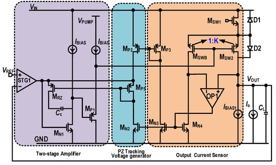
Figure 2.
Typical traditional pole–zero tracking compensation circuit.
The pole–zero (PZ) dynamic compensation is realized by the output current sensor, PZ tracking voltage generator, MRZ and CC circuits. The current sensor mirrors and tracks the output current and realizes 1/K current scaling by adjusting the mirror ratio of MSWB and MSW2. The drain voltages of MSWB and MSW2 are equal through the function of OP1, achieving accurate copying of the current, which is subsequently output through the current mirror composed of MN3 and MN4. The current of MP5 is the output of MP2 and MP3 current mirrors. As a result, the VGS voltage of MP5 is proportional to the output current. In addition, MRZ and CC form a zero, and the gate–source voltages of MRZ and MP5 are the same, which makes the on-resistance of MRZ proportional to the output current. When the output current decreases, the output pole (Po) and the VGS voltage of MP5 decrease. With a larger impedance of MRZ, the frequency of the zero formed by MRZ and CC is lowered, realizing the tracking compensation of the output pole. The compensated voltage stabilizing loop has only one dominant pole at the output of EA1, which makes the entire loop stable.
From the above analysis, there exist two dominant poles located at VOUT and EA1 in the traditional circuit with varying load current. In addition, the Po at the VOUT terminal will change with the varying load current. For example, with a small output current, RL >> RMSW2 (meanwhile, RMSW1 << RMSW2), and the output impedance at the VOUT terminal is:
The VGS voltage of MP5 is calculated as:
Since the VGS values of MRZ and MP5 are the same, and MRZ is operating in the linear region, the on-resistance of MRZ is:
Thus, the zero formed by MRZ and CC can be expressed as:
The K in Equations (3)–(5) represents the ratio of sensor current, and WMP5 and LMP5 are the channel width and length of the MP5 transistor. The frequency compensation can be achieved by using ZC to cancel out Po. However, due to the different dependence of Po (Equation (2)) and ZC (Equation (5)) on RL, ZC cannot track the change of Po well when RL varies in a large range. This can further result in a large change in bandwidth as well as a deterioration in stability.
3. Proposed Regulation Circuit with Adaptive Linear Pole–Zero Tracking Compensation
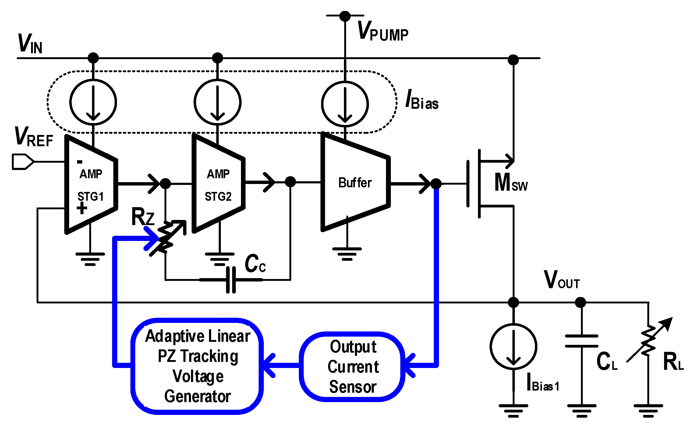
To solve the above issue, we propose a regulation circuit with an adaptive linear pole–zero tracking compensation, which is schematically illustrated in Figure 3. The entire circuit includes a two-stage amplifier (AMP STG1 and AMP STG2), buffer stage, output current sensor, adaptive linear PZ tracking voltage generator, output power transistor and load resistor and capacitor. Among these components, the AMP STG1 provides gain and the AMP STG2 provides low output impedance to push the output pole farther from the origin. The output power transistor provides a large current, and the output current sensor can achieve accurate reproduction of the output current. The adaptive linear PZ tracking voltage generator is used to perform the compensation of the output pole making the unity-gain bandwidth (GBW) of the feedback system constant while ensuring stability.
Figure 3.
Proposed structure of regulation circuit with the adaptive linear pole−zero tracking compensation. (RZ is the equivalent impedance of the NMOS MRZ; IBias and IBias1 are bias currents. VPUMP is the high−level supply voltage in the USB interface protecting circuit.)
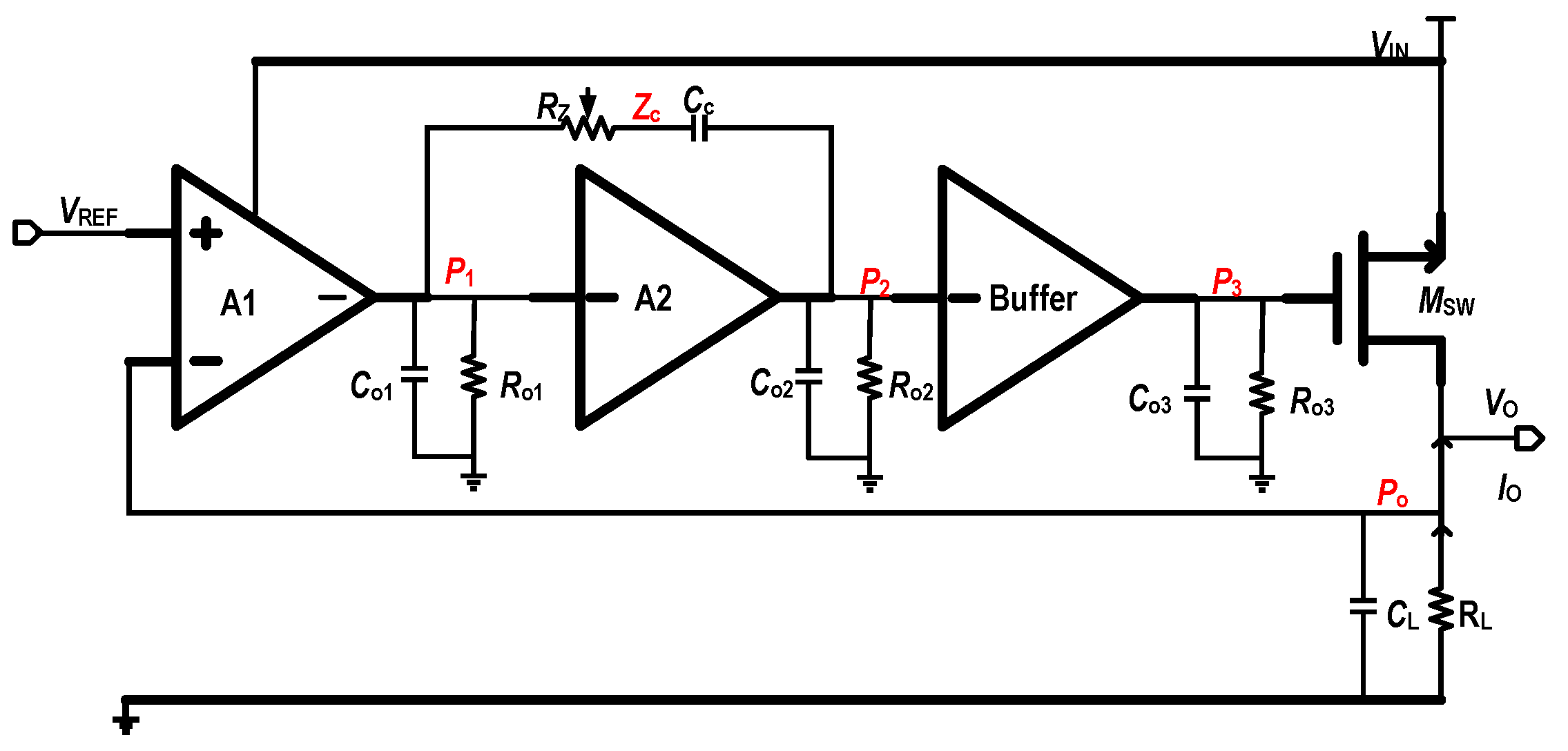
Figure 4 shows the pole−zero distribution of the proposed regulation circuit. There are four poles (P1~P3, Po) and a zero (ZC) in the circuit illustrated in Figure 3.

Figure 4.
The pole–zero distribution of the proposed regulation circuit.
The four poles can be expressed as:
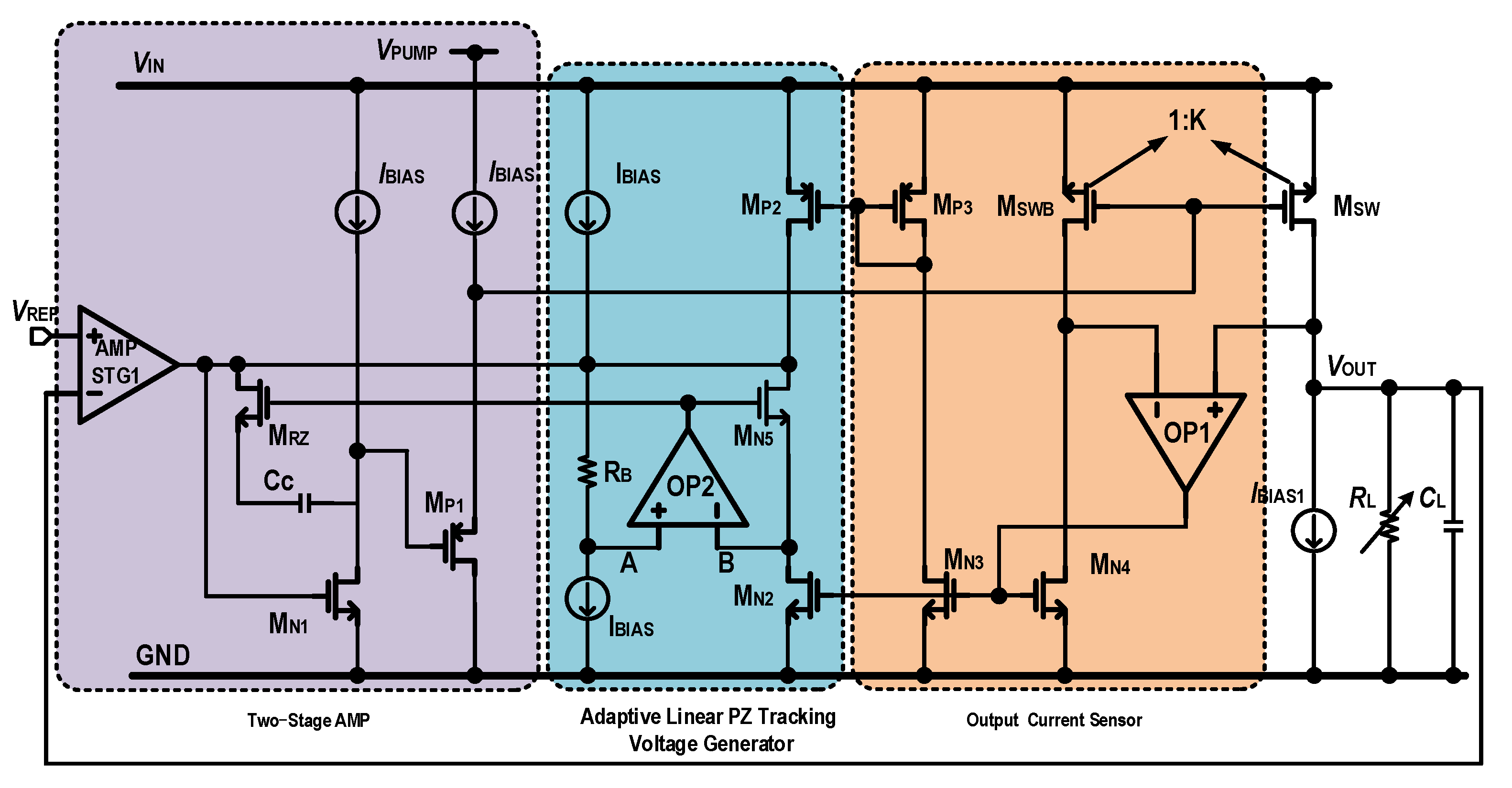
Figure 5 shows the detailed structure of the adaptive linear pole–zero compensation voltage regulation circuit (MSW1 and MSW2 are represented and labeled by MSW for a better description). The linear pole–zero tracking voltage generator is composed of OP2, MN5 and RB. The voltage potential at points A and B are clamped to be equal though OP2, which makes the VDS voltage of MN5 equal to the voltage across RB, VDSN5 = VRB. MN5 can be modulated to work in the linear region through VRB making VDSN5 = VRB = Vdrop. The output of OP2 also functions as the gate voltage of both MRZ and MN5.
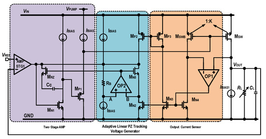
Figure 5.
The detailed structure of the linear adaptive pole–zero compensation voltage regulation circuit.
From the circuit shown in Figure 5, MN5 is in the linear region, and the drain–source current of MN5 is:
There is a fixed 1/K relationship between the drain–source current of MN5 and the output current due to the current mirror:
From Equations (10) and (11), the VGS of MN5 transistor is:
Considering the fact that the VGS values of MRZ and MN5 are the same, and both work in the linear region, the on-resistance of MRZ can be obtained by:
From Equations (11)–(14), we can obtain:
The corresponding zero can be obtained from Equation (15):
Compared to the traditional circuit design, in our proposed circuit design, both Po and ZC are in a first-order linear relationship to RL, as indicated by Equations (9) and (16), respectively, realizing the linear tracking and compensation of ZC with a different loading current.
4. Simulation and Experimental Test Results
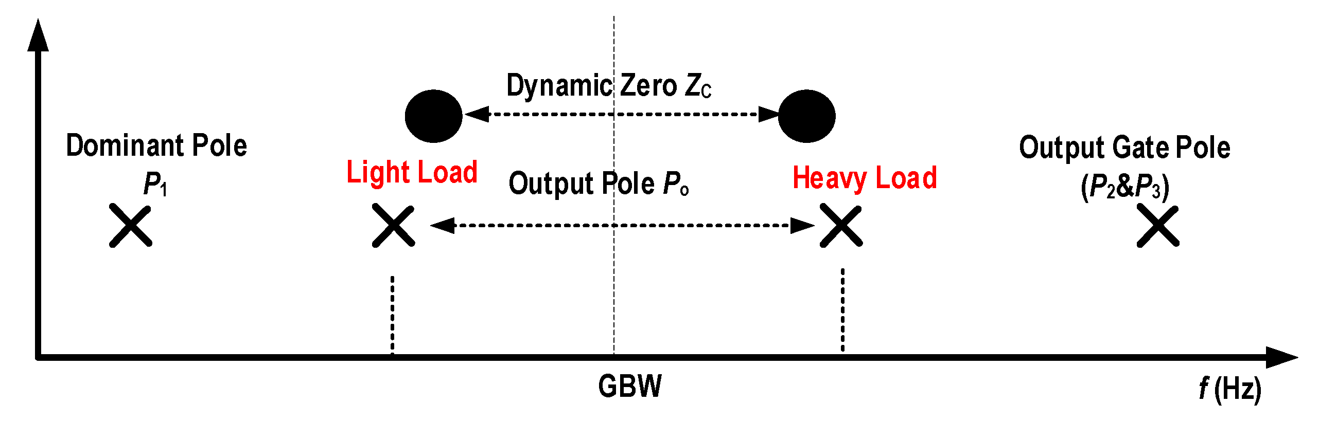
The positions of the poles are the outputs of each stage with P1 as the dominant pole and Po as the first nondominant pole. P2 and P3 are far away from P1 due to the small equivalent input capacitance and equivalent output impedance, and do not affect the stability of the loop. Then, we can plot the location of the poles of the proposed regulation circuit as shown in Figure 6. From Equations (9) and (16), it can be seen that both ZC and Po have a first-order linear proportional relationship with IO. When the load changes, ZC can be used to track and compensate for the change of Po linearly. Thus, we can obtain a high-stability loop in a wide current range.
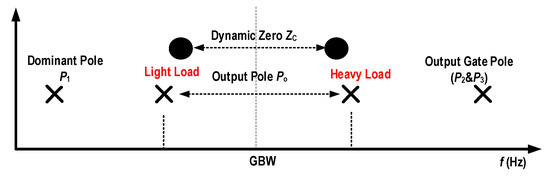
Figure 6.
The location of the poles of the proposed regulation circuit.
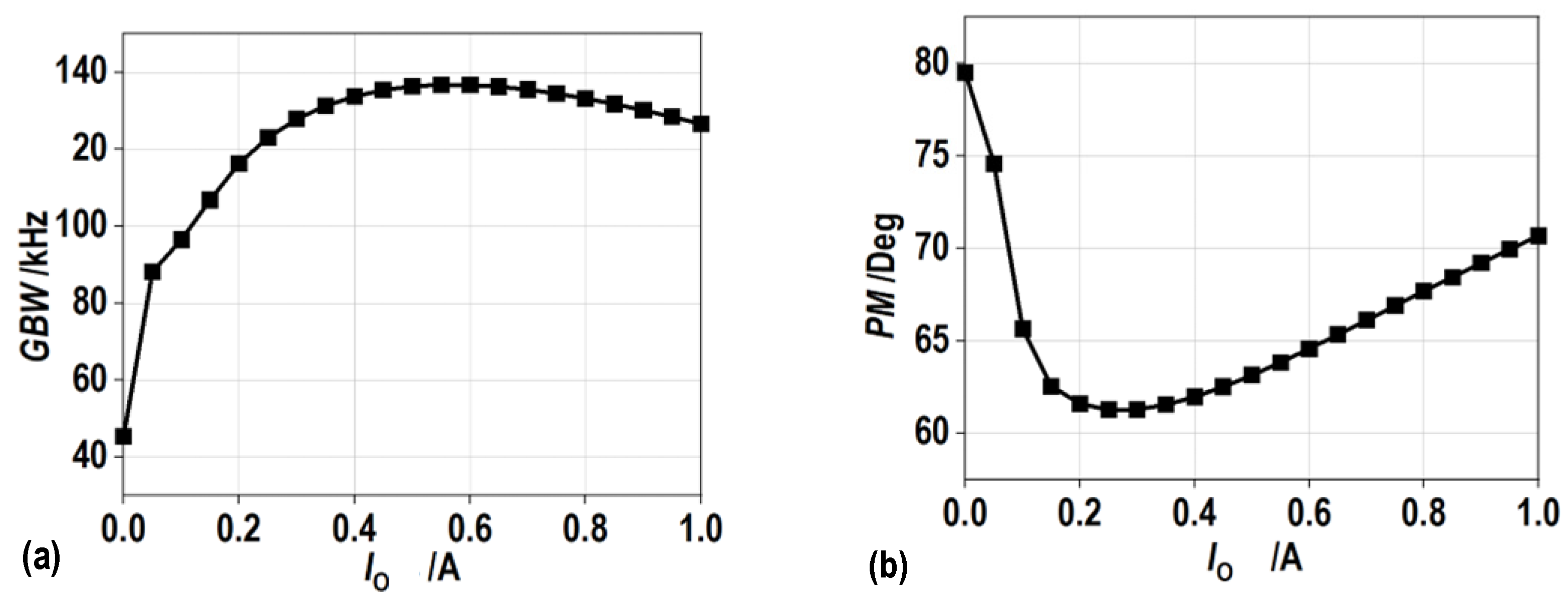
Figure 7 shows the continuous change of GBW and the phase margin under different load currents. The current changes from 0 A to 1 A, and the GBW changes from 45 kHz to 135 kHz. The phase margin is greater than 60° in the full current range ensuring excellent loop stability.
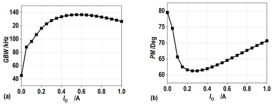
Figure 7.
The simulation results of (a) GBW and (b) phase margin with IO from 0 A to 1 A.
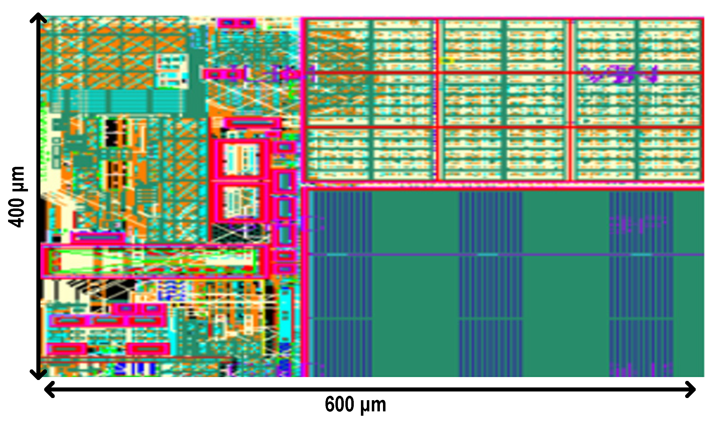
The proposed high−stability regulation circuit was designed in a 180 nm CMOS process. The chip micrograph is shown in Figure 8, and the die size is 400 × 600 μm2.

Figure 8.
The chip micrograph.
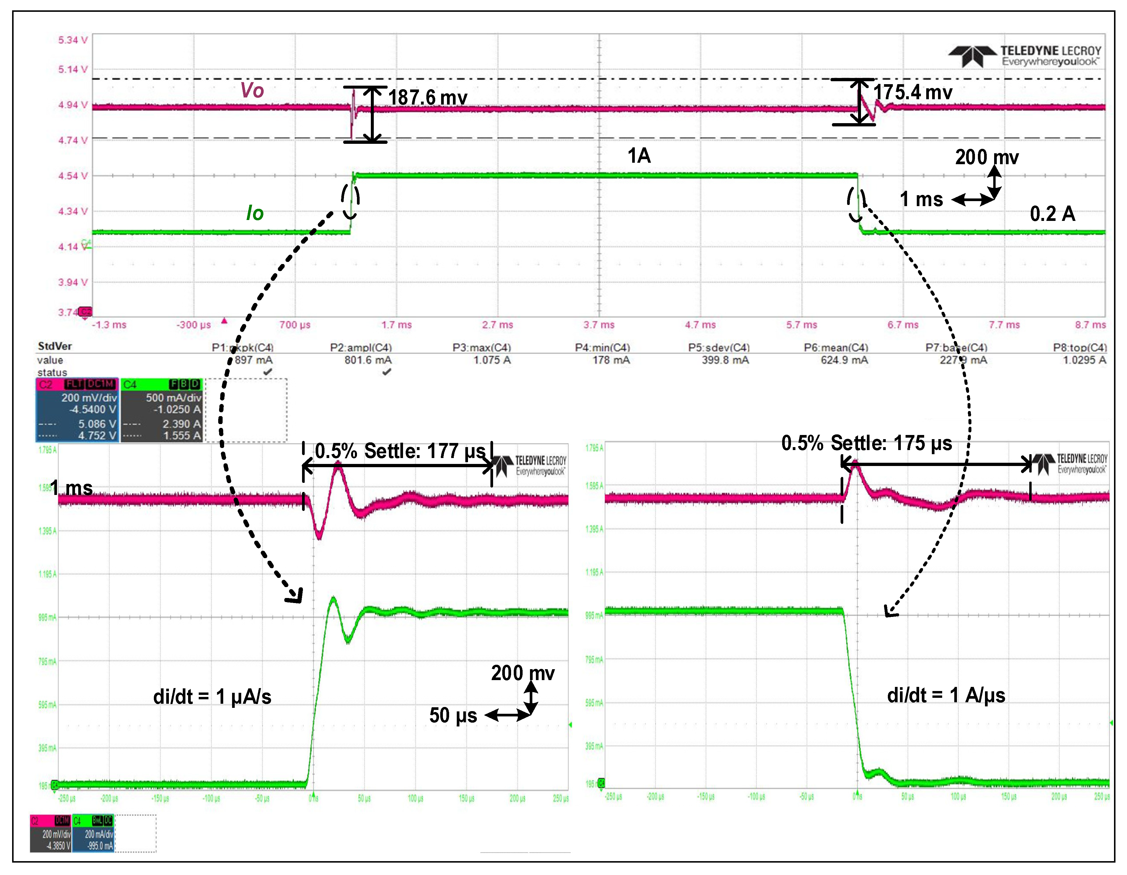
Figure 9 shows the measured load transient responses when the load changes between 0.2 A and 1 A. From the figure, the output VO shows undershoot and overshoot voltages of −187.6 mV and 175.4 mV, respectively. The 0.5% settling times are 175 μs and 177 μs, respectively. The test result indicates an enhanced working stability of the entire loop.
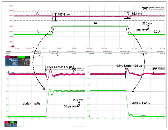
Figure 9.
Measurement output voltage VO and output current IO waveforms under load transitions between 0.2 A and 1 A.
Finally, we compared the performance that can be achieved by the currently reported compensation methods of voltage stabilization loops. The comparison is listed in Table 1 in terms of process, dropout voltage, output capacitor and the maximum output current Io(max). From the comparison result, it is found that within the full load range, the bandwidth change of the regulation circuit proposed in this paper is the smallest, the stability of the system is better and a smaller drop voltage can be achieved.

Table 1.
Comparison Table.
5. Conclusions
In summary, an adaptive linear pole–zero tracking compensation was proposed in this paper, by changing the tracking transistor from the traditional saturation region to the triode region for a good linear match to the resistance of the zero-adjusting resistor. The frequency change of the zero and the first nondominant pole was linearly consistent. From the simulation and test results, the bandwidth change range was very small within the full load range, due to the high linearity of the zero and the first nondominant pole with the load change. Further delicate circuit design and engineering will shed more light on this issue towards advanced USB Type-C interface applications.
Author Contributions
Conceptualization, H.T.; methodology, H.T.; software, H.T.; validation, H.T.; formal analysis, H.T.; investigation, Y.W.; resources, Y.W.; data curation, Y.W.; writing—original draft preparation, Y.W.; writing—review and editing, Y.W.; visualization, Y.W.; supervision, D.W.Z.; project administration, D.W.Z.; funding acquisition, D.W.Z. All authors have read and agreed to the published version of the manuscript.
Funding
This research received no external funding.
Data Availability Statement
No new data were created or analyzed in this study. Data sharing is not applicable to this paper.
Conflicts of Interest
The authors declare no conflict of interest.
References
- He, F. USB Port and power delivery: An overview of USB port interoperability. In Proceedings of the 2015 IEEE Symposium on Product Compliance Engineering (ISPCE), Chicago, IL, USA, 18–20 May 2015; pp. 1–5. [Google Scholar]
- Kwok, K.C.; Mok, P.K.T. Pole-zero tracking frequency compensation for low dropout regulator. In Proceedings of the I 002 IEEE International Symposium on Circuits and Systems (ISCAS), Phoenix-Scottsdale, AZ, USA, 26–29 May 2002; pp. 735–738. [Google Scholar]
- Rajput, S.K.; Hemant, B.K. Two-stage high gain low power OpAmp with current buffer compensation. In Proceedings of the 2013 IEEE Global High Tech Congress on Electronics, Shenzhen, China, 17–19 November 2013; pp. 121–124. [Google Scholar]
- Ho, M. A CMOS Low-Dropout Regulator with Dominant-Pole Substitution. IEEE Trans. Power Electron. 2016, 31, 6362–6371. [Google Scholar] [CrossRef]
- Duan, Q.; Li, W.; Huang, S.; Ding, Y.; Meng, Z.; Shi, K. A Two-Module Linear Regulator with 3.9–10 V Input, 2.5 V Output, and 500 mA Load. Electronics 2019, 8, 1143. [Google Scholar] [CrossRef] [Green Version]
- Jiang, Y.; Wang, L.; Wang, Y.; Wang, S.; Guo, M. A High-Loop-Gain Low-Dropout Regulator with Adaptive Positive Feedback Compensation Handling 1-A Load Current. Electronics 2022, 11, 949. [Google Scholar] [CrossRef]
- Duong, Q.H.; Nguyen, H.H.; Kong, J.W.; Shin, H.S.; Ko, Y.S.; Yu, H.Y.; Lee, Y.H.; Bea, C.H.; Park, H.J. Multiple-loop design technique for high-performance low dropout regulator. In Proceedings of the 2016 IEEE Asian Solid-State Circuits Conference (A-SSCC), Toyama, Japan, 7–9 November 2016; pp. 217–220. [Google Scholar]
- Sobhan Bhuiyan, M.A.; Hossain, M.R.; Minhad, K.N.; Haque, F.; Hemel, M.S.K.; Md Dawi, O.; Ibne Reaz, M.B.; Ooi, K.J. CMOS Low-Dropout Voltage Regulator Design Trends: An Overview. Electronics 2022, 11, 193. [Google Scholar] [CrossRef]
- Nozahi, M.; Amer, A.; Torres, J.; Entesari, K.; Sanchez-Sinencio, E. High PSR Low Drop-Out Regulator with Feed-Forward Ripple Cancellation Technique. IEEE J. Solid-State Circuits 2010, 45, 565–577. [Google Scholar] [CrossRef]
- Huang, C.; Ma, Y.; Liao, W. Design of a Low-Voltage Low-Dropout Regulator. IEEE Trans. Very Large Scale Integr. (VLSI) Syst. 2014, 22, 1308–1313. [Google Scholar] [CrossRef]
- Cao, H.; Yang, X.; Li, W.; Ding, Y.; Qu, W. An Impedance Adapting Compensation Scheme for High Current NMOS LDO Design. IEEE Trans. Circuits Syst. II Express Briefs 2021, 68, 2287–2291. [Google Scholar] [CrossRef]

Publisher’s Note: MDPI stays neutral with regard to jurisdictional claims in published maps and institutional affiliations. |
© 2022 by the authors. Licensee MDPI, Basel, Switzerland. This article is an open access article distributed under the terms and conditions of the Creative Commons Attribution (CC BY) license (https://creativecommons.org/licenses/by/4.0/).