Article

Super Directional Antenna—3D Phased Array Antenna Based on Directional Elements

1
Faculty of Engineering, Ariel University, Ariel 40700, Israel
2
Afeka College of Engineering, Tel Aviv 6910717, Israel
*
Author to whom correspondence should be addressed.
Electronics 2022, 11(14), 2233; https://doi.org/10.3390/electronics11142233
Submission received: 9 May 2022 / Revised: 3 July 2022 / Accepted: 7 July 2022 / Published: 17 July 2022

Abstract

:
This paper describes an antenna design approach for achieving super directivity in an AESA (Active Electronic Scanned Array) radar using an unconventional 3D phased array (PA) antenna concept based on directional Yagi–Uda elements. The proposed scheme is shown to have a wider scanning feature, with higher directivity in comparison to the same geometry dipole array without increasing the element number. The antenna’s microwave design includes an antipodal Yagi–Uda antenna element that is implemented efficiently on a microstrip PCB using a balun (balance–unbalance)-fed network. This type of antenna is valuable in restricted aperture scans for achieving a narrow antenna beam that increases the angular resolution and measurement precision of tracked targets and also enlarges the detection range or, alternatively, achieves the same performance with a lower number of elements—meeting the goal of low-cost production. The notable result of the high antenna directivity was obtained by both the element and the array architecture, which allowed for improvements in the Array Factor (AF) directivity by increasing the element’s spacing and broadening the scan sector, achieved via the suppression of the element’s Grating Lobe (GL). Another important benefit of this antenna design is the superior coupling reduction caused by its enlarged element distances, which are very significant in electronic scans. An outstanding opportunity to exploit this low coupling can be found in separated MIMO radar architecture. Other benefits of this design’s architecture are the support of a combined module and antenna on a unified board thanks to the End-Fire radiation pattern, its low frequency sensitivity, and its low-cost manufacturing.

1. Introduction

Phased Array (PA) Steering Antenna Technology is conventionally used in the military for radar and satellite applications [1] and is nowadays also a trend in new applications for commercial purposes, due to the growing need for higher data rates in communication devices such as 5G cellular devices and the IoT [2]. This technology has a lot of performance advantages in comparison to conventional mechanical scan antennae [3], such as multifunctionality, switching beams, supporting desired scan times, the ability to track a high number of targets, flexibility in using special and dedicated beams with adequate waveform parameters according to the target demand, nulling [4], improved system reliability achieved by the avoidance of moving parts, and graceful degradation [5]. The performance of an AESA antenna is widely affected by many technical parameters [6], such as the grid type, the distance between elements, the element directivity, the bandwidth, the scan angle aperture, and the coupling between elements—which is usually an undesired physical phenomenon that is difficult observe analytically [7].
It is common to implement an antenna array in order to achieve wide spatial coverage by using omni directional antenna technologies, such as a patch or dipole antenna distanced by λ / 2 between each element [8]. Unfortunately, this type of array has low directivity and therefore suffers from major disadvantages such as needing a high element number or higher element power, with severe cooling requirements for avoiding phase deviations—which spoil the monopulse angle measurement. Super-directive arrays have been popular in the academic world since they provide higher directivity than uniformly excited antenna arrays of the same length. Considerable research on the possibilities of super-directive arrays has been carried out over the years, finding theoretical limits such as the Array Pattern (AP) and directivity versus the distance between elements, the tolerance, and the bandwidth under different assumptions [9]. Some other studies have used optimized polynomial techniques to generate super-directive array functions by changing the number of elements and array length with altered array parameters [10] or denser elements [11]. Studies show that reasons for avoiding directional elements in classical PAs include both the coupling that occurs between elements that affects the AP and angular scan restriction due to the element pattern (EP) [7].
The present paper proposes a new approach for designing an AESA antenna coverage range, assuming a given number of elements, by developing an uncommon 3D array based on a directional Yagi–Uda element with an H-pattern of ± 20 ° [12]. Consequently, a very high antenna gain was achieved in both the transmit and receive modes. The main principle that enabled these super directivity linear feed antennas depended on the unchanged element’s directivity in comparison to the complicated techniques of Parasitic Loaded Super-Directivity [13] and feed structures with a variable phase [14]. The element directivity was doubly exploited to both achieve high system gain and to suppress the Grating Lobes (GL), which allowed for increases in the azimuth AF (Array Factor) directivity by increasing the azimuth element distances from 0.75 λ in a conventional scanned array by ± 20 ° , up to λ .
The CST results for a 4 × 4 Yagi–Uda element array with a distance of λ between adjacent elements showed the achievement of a narrow azimuth and elevation beam width and, consequently, high directivity improvement-including coupling-in comparison to standard dipole arrays. Better performances could certainly be reached in separated radar architecture [15]-utilizing MIMO radar techniques [16] by spacing the element grid to an equivalent 2 λ to significantly reduce the coupling to neglected values of less than −30 dB. Consequently, the high AP achieved increased the detection ranges, with a significantly lower RF intensity for each element-or, alternatively, achieved the same performance with a lower number of elements, according to the radar equation [17]. Another benefit of this antenna structure is the opportunity of supporting a combined module and antenna on a unified board thanks to the End-Fire radiation pattern [18], which makes it cheap and makes mass production possible.
The selected element type was based on a Yagi–Uda antenna that was efficiently implemented on a microstrip PCB using an optimal balun [19] (balance–unbalance)-fed network with an antipodal antenna. This type of antenna was selected due to its high directivity, narrow band, and End-Fire radiation pattern. The antipodal implemented the dipole on two different microstrip layers: one on the top and the other on the bottom, achieving high isolation between the left and right parts of the dipole. This implementation also reduced the element size thanks to the 180 ° phase shifter (PS) and splitter elimination, while also efficiently improving the element. In [20], balun implementation of a dipole with a taper ground was suggested, but it was found to be inefficient-presenting with back transmitting-and therefore, we instead the use of a superior rectangular ground.
This paper is divided into three sections: In the first section, we state the background of the super directive array theory and describe the design algorithm and simulation. In the second section, we show a design of a 3D directional Yagi–Uda element and array using CST simulation software and compare it to a dipole array. In the third section, the directional 3D Yagi–Uda array and the dipole array are measured and compared in a configuration of two-dimensional element spacing of λ in azimuth and 0.7 λ in elevation. Finally, an equivalent 2 λ spacing is suggested for separated MIMO radars with independent coupling.

2. Background

2.1. Super Directive Array Theory

The AP is the product of the Element Pattern (EP) and the AF, assuming no coupling between elements, where the AP corresponds to the total array pattern. The AF is a mathematical representation of the array gain and the EP corresponds to the element pattern [21,22].
The following AP equation was used, shown in Equation (1):
A P ( e l , a z ) = A F ( e l , a z ) E P ( e l , a z )
The system coordination that was selected for the array simulations is depicted in Figure 1 and was fit to the elevation and azimuth parameters, with the following equations and results presented accordingly:
The AF is expressed as:
A F   ( e l , a z ) = n = 1 N e I n ( x n , z n ) e j k { x n cos ( e l )   sin ( a z ) + z n sin ( e l ) }
where x n ,   z n are the element positions on the X–Z plane, I n is the excitation coefficients, N e is the number of elements, and k is the wave number.
When scanning, an additional phase will be added to I n as follows:
I n ( x n , z n ) = W n ( x n , z n ) e j k { x n cos ( e l 0 ) sin ( a z 0 ) + z n sin ( e l 0 ) }
where W n is the element tapering and a z 0 ,   e l 0 expresses the scanned direction in the azimuth and elevation, correspondingly. Substituting Equation (3) for (2) we get:
A F   ( e l , a z ) = n = 1 N e W n ( x n , z n ) e j k [ x n { cos ( e l ) sin ( a z ) cos ( e l 0 ) sin ( a z 0 ) } + z n { sin ( e l ) sin ( e l 0 ) } ]
The common element type used in PA is omni-directional, with a typical gain of 4–5 dB [23] for lower scan sensitivity and to avoid coupling effects. Therefore, the AP is determined mostly by the AF and not by the EP, which is ideally isotropic. The known array beamwidth approximation for an omni-directional, lossless, array-based antenna is expressed as follows:
θ 3 d B   λ D [ r a d ] = 57 λ D [ d e g ]
The approximate relationship between the E-plane beamwidth B W E , the H-plane beamwidth B W H , and a gain of a surface-wave antenna depends only on the array aperture, according to the following equation [24]:
G     4 π D x D z λ 2   30000   B W E   B W H
Assuming a one-dimensional azimuth scan and keeping the element spacing d as 0.75 λ , we avoid GL in the desired scan of ± a z = 20 ° —according to Equation (7) for an omni-directional element-based array [25].
d < λ 1 + | sin ( a z ) |
In this paper, we show that Equation (7) is not suitable for a directional-based array, which could achieve better results in both gain and scanning aperture. The following section will detail the key idea and the design algorithm for analyzing this.

2.2. Super Directive Array Design Algorithm

Since a restricted scan aperture is required, high antenna directivity is achievable-improving the AF directivity by increasing the element spacing and broadening the scan sector thanks to the element’s GL suppression. To find the parameters of the AF according to the desired optimization goal of the AP, we use Equation (4), where N x ,   N z are the number of elements on the z-axis and x-axis, correspondingly, and d x ,   d z are the element spacing defined by d x = x n x n 1   and   d z = z n z n 1 . While using a directional element pattern in an antenna array, we can achieve both higher systems gain and an extended scan aperture in comparison to a dipole array with the same geometry. This enhanced performance is achieved thanks to the high element directivity and the GL suppression, which allow for increases in the AF directivity by increasing element distancing. The flow chart in Figure 2a shows an algorithm for designing a super-directive array according to the system design goals. Figure 2b,c show an example of designing a directive array with a 10 ° azimuth scan while meeting the design goal of a peak-to-sidelobe (PSL) larger than 10. The selection of the design working point is dependent on the optimization goal and will be detailed in Section 3.

3. Yagi–Uda Array Element

The selected element type was a Yagi–Uda antenna due to its high directivity, high efficiency, narrow band demand adequate for the PA and radar limitations, and an End-Fire radiation pattern for unified module realization. The procedure of the Yagi–Uda antenna design included a microstrip dipole pre-design with the further addition of directors for optimal performance in terms of the Return Loss, directivity, and a beamwidth matching a 40 degree ± 20 ° scan range. The microwave design method consisted of quarter wave matching with driver- and director-tuning optimization, meeting the bandwidth demand. This implementation method utilized the efficient design of a balun-fed network to reduce the element size by eliminating the needs of the RF-splitter and 180 ° PS, as well as to reduce the transmission line losses and errors from the PS corners. The antipodal antenna implemented the dipole on two different microstrip layers-both on the top and on the bottom-achieving high isolation between the left and right parts of the dipole and providing another design optimization parameter, as shown in Figure 3.
The antenna’s system design requirements are shown in Table 1:

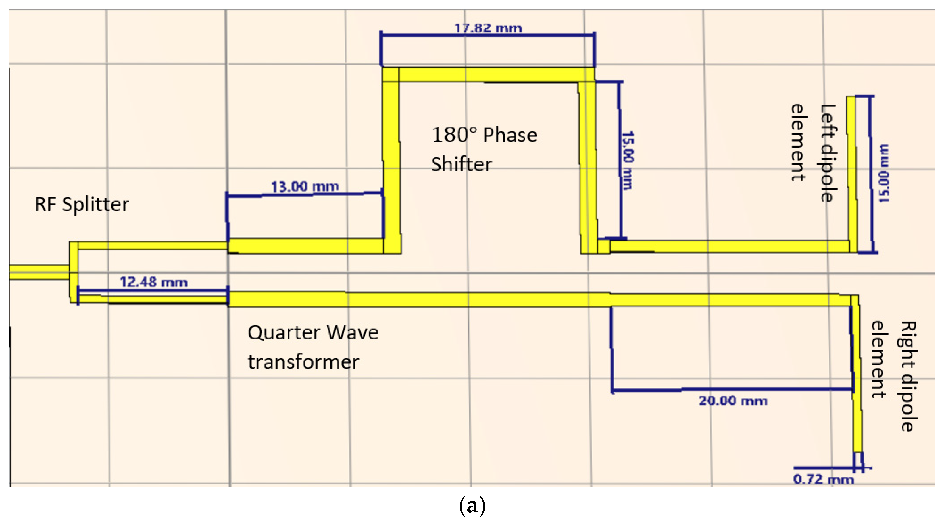
3.1. Typical Element

The element’s design requirements are shown in Table 2:
The dipole pre-design antenna simulation using CST software achieved the results in Figure 4 with the parameters that is shown in Table 3.

3.2. Directive Element

The design of the 3D super-directive antenna included multi-objective optimization, finding that the parameter set in Table 4 and Figure 5 brought the desired directivity, Return Loss, and Beamwidth according to the design requirements.
Simulating with high dense meshing on the conductors, we obtained the results in Figure 6:
From the cartesian plots, we see that the peak-to-sidelobe (PSL) ratio in the azimuth axis was ~25 dB, which was much higher than the elevation’s PSL of ~10 dB. Consequently, further GL suppression by the element is possible in the azimuth axis, and thus, higher distancing between elements in this direction is also possible.

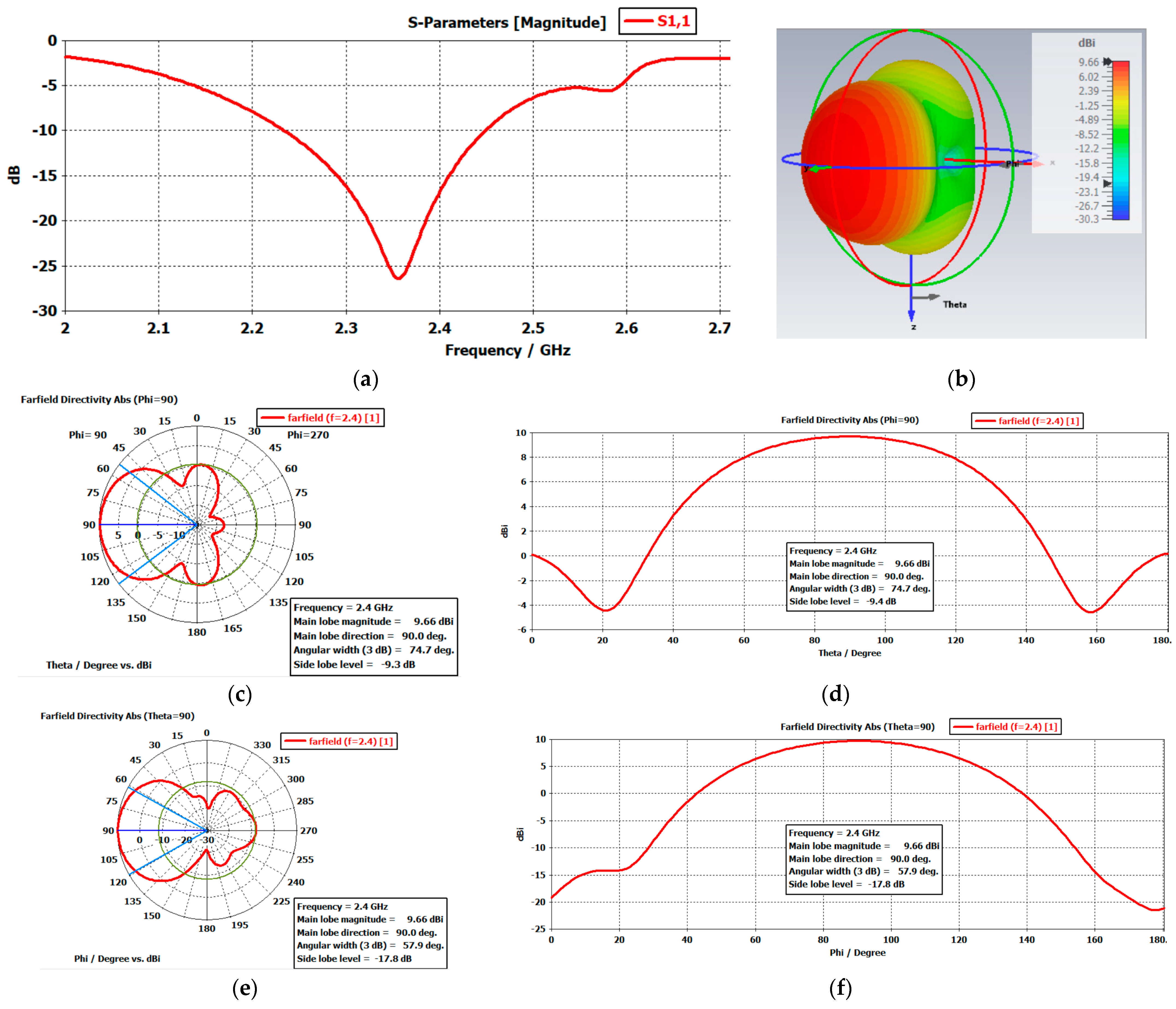
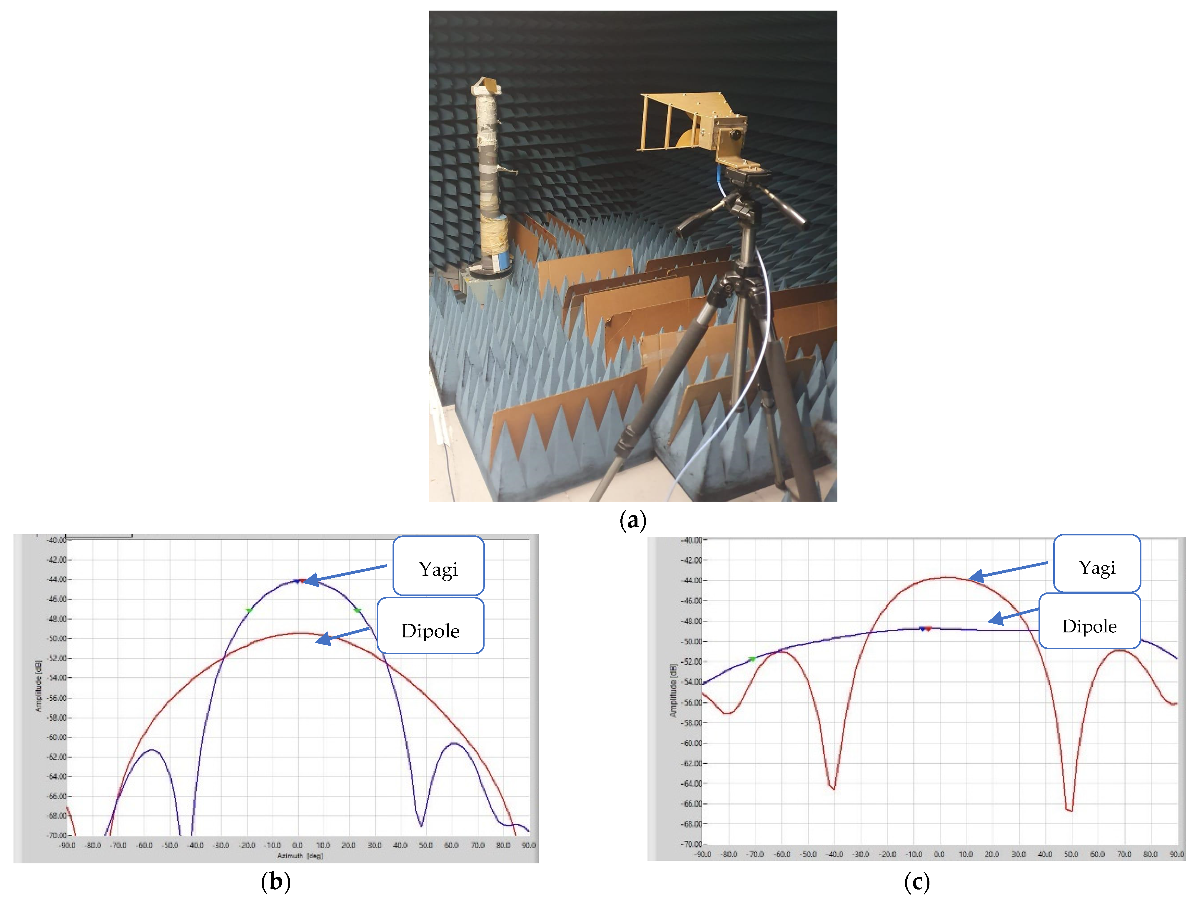
3.3. Element Measurement

3.3.1. Coupling Measurements

Mutual coupling between elements in an antenna’s array is an undesired physical phenomenon that is difficult to analytically observe. The coupling of a typical dipole depends on various parameters such as impedance matching and directivity degradation, which are exponentially affected by the element distances [7] and are severely impaired when scanning. Further distancing of the elements due to the element pattern results in the major accomplishment of reductions in undesired coupling.
For estimating the coupling, we built a test model of a Yagi–Uda antenna [26] with a similar gain and beamwidth (but different line widths as a PCB was not used) and measured its mutual coupling (S21) using a Network Analyzer in both the vertical and horizontal positions. From the measured results of the following setups, shown in Table 5 and Figure 7, we could infer that the adjacent elements distanced above 1.5 λ had neglected mutual influences ( < 30   d B ) .

3.3.2. Gain and Beamwidth Measurements

We measured the antenna’s element gain in the Farfield Chamber and computed the antenna’s gain and bandwidths. The measurements were performed with the MiDAS tool [27] and compared to a reference antenna. Corresponding to the RF simulation, the achieved results of the directional antenna had a larger directivity of 5   d B in both the azimuth and elevation as shown in Figure 8.

3.4. Algorithm for the Array Pattern Simulation

Taking the antenna’s element pattern results from CST, and assuming no coupling, we simulated for the super-directivity domain D ( a z 0 , e l 0 , d x , d z ) that would meet the system requirement of P S L > M   d B , where M is a systematic parameter requirement. The following scheme in Figure 9 was achieved for the simulation of a 2-dimensional domain of the designed dipole and Yagi–Uda elements. According to the graph, we can see that a typical phased array, based on a dipole antenna with d x = λ / 2 , has a wider scan aperture than a Yagi–Uda antenna at point A, due to the Yagi–Uda pattern. However, at point B, where d x = λ , the directional antenna had an ability to scan up to ± 35 ° —thanks to the GL suppression by the directive element pattern, where the dipole antenna has no possibility of scanning. When d x = 1.4 λ (point C), we achieved the largest azimuth gain of the Yagi–Uda array-with the maximum azimuth gain according to Equation (6)—at the expense of the possibility of having no scan benefits.
The presented paper compared the performances of an equivalent Yagi–Uda array and dipole array, elaborating on the electromagnetic simulations and measurements with d x = λ (point B), to show both gain and scan benefits.

4. Three-Dimensional Active Electronic Scanned Array Simulations

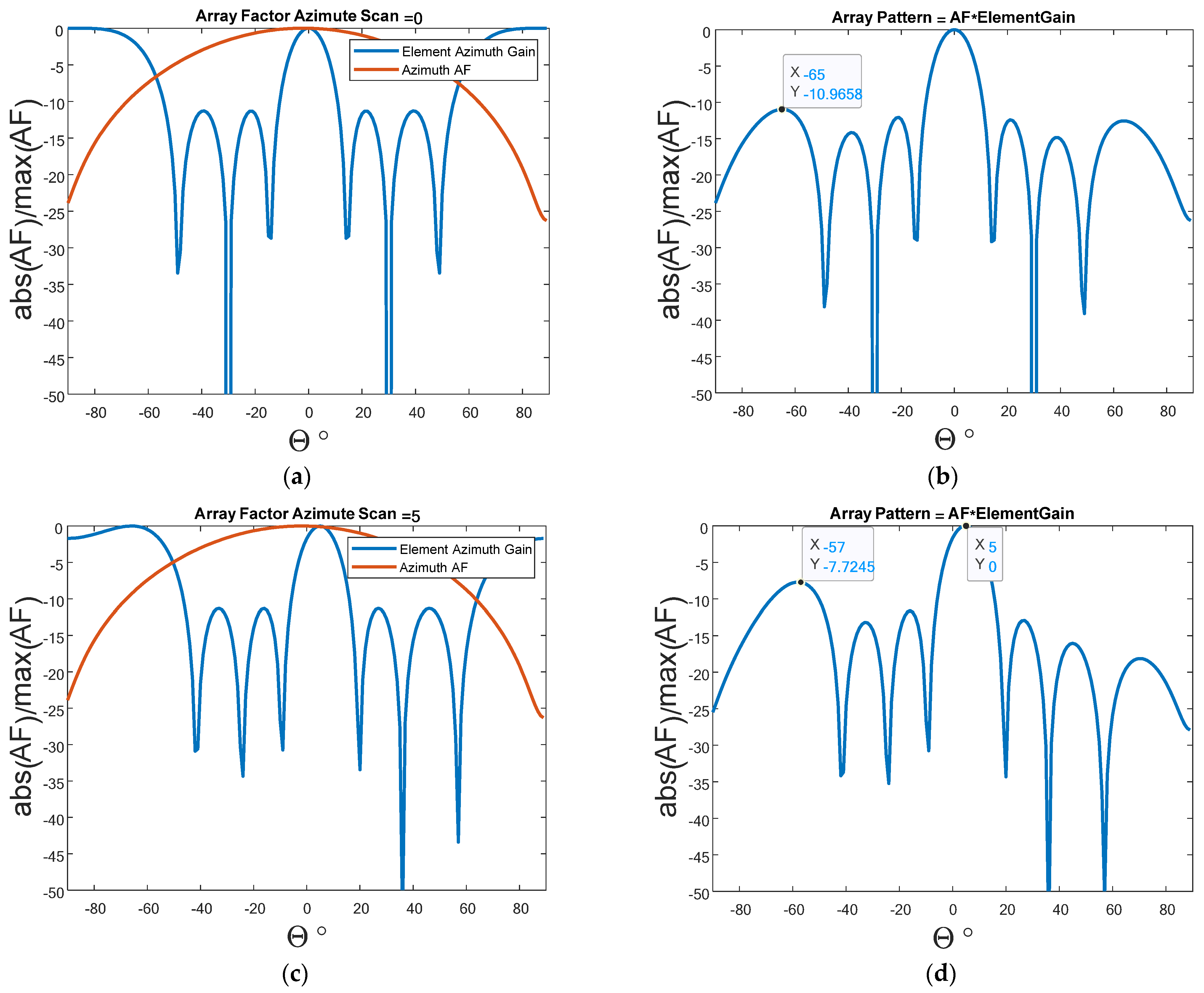
4.1. Array Factor and Array Pattern Simulations

AF is a mathematical representation of the array gain constructed only by the element’s phase superposition, which is affected by the element’s geometric position. In a standard AESA, the AF is the critical component that determines the array performance due to its omni-directional element pattern. Unlike in usual cases, our Yagi–Uda element pattern had directivity, and thus, this had to be taken into consideration. The full antenna’s AP was a product of the electromagnetic element simulation taken from CST and the MATLAB simulation of the AF. Simulating an array of a 4 × 4 horizontal dipole (Figure 10) and the Yagi elements (Figure 11) with d x = λ , d z = 0.7 λ , we obtained the following results for the AF and AP for azimuth angles of 0, 10, and 15.
We can see that in the same geometry, scanning with the dipole array was impossible due to its having a PSL that is lower than that required, while the Yagi–Uda array had a scanning possibility of ± 15 ° . It should be noted that the azimuth was focused due to the large element distance.

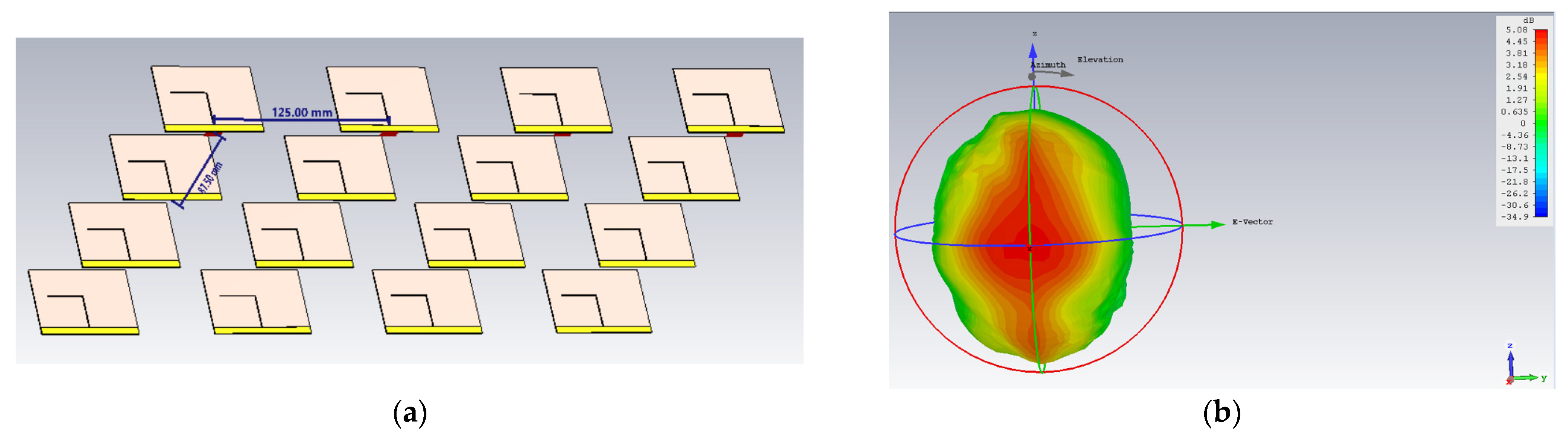
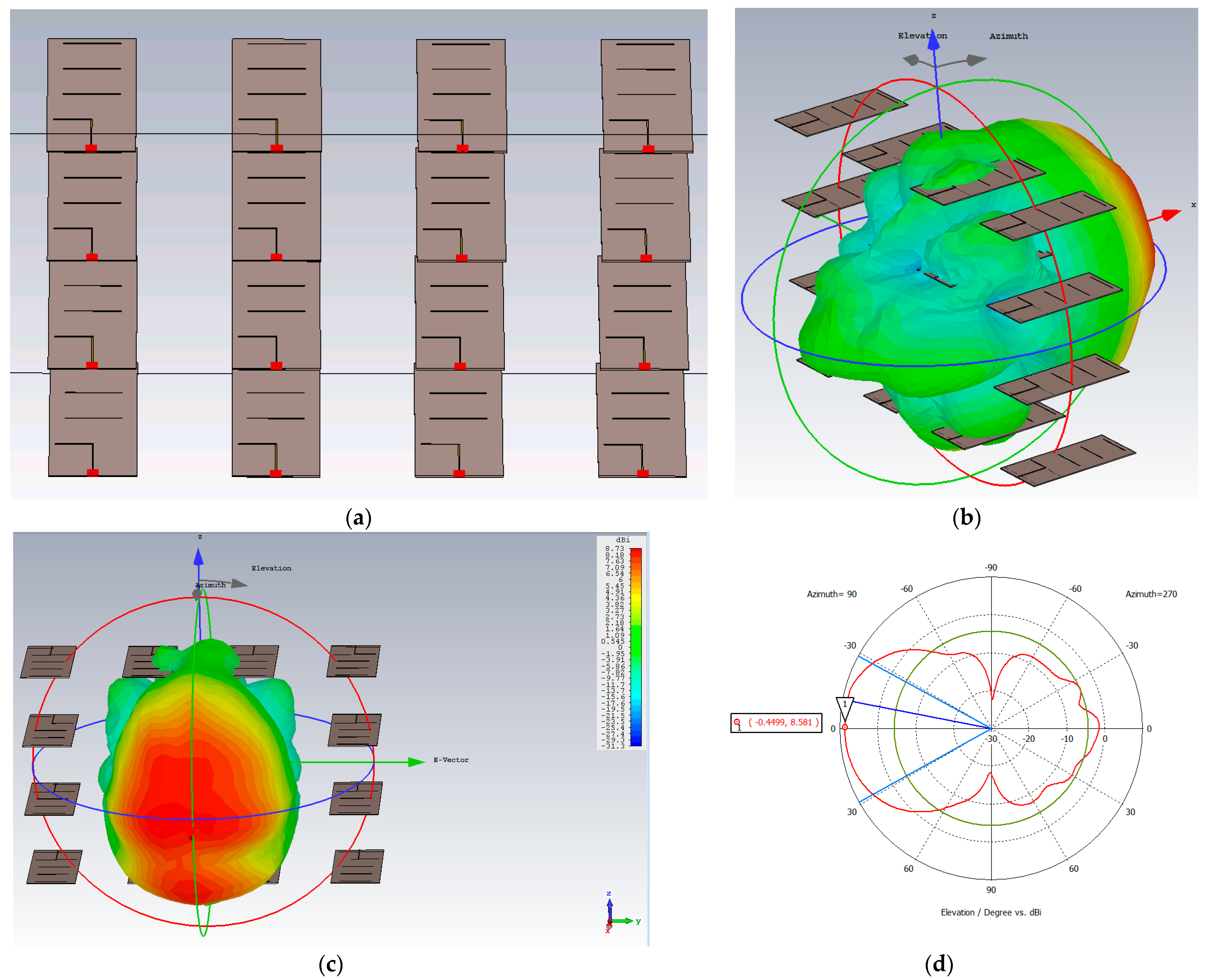
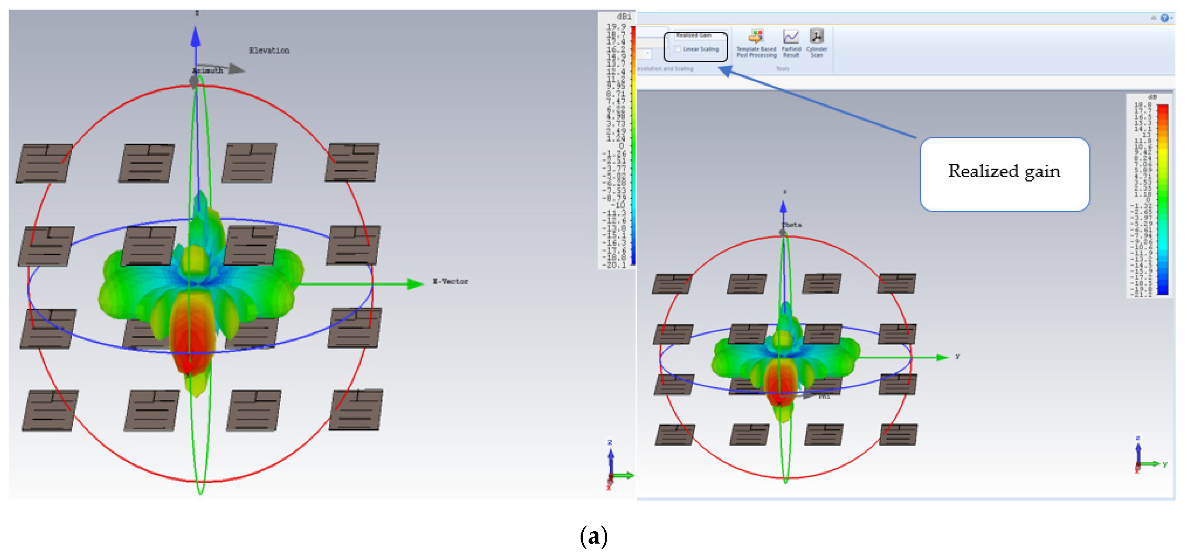
4.2. Dipole and Yagi–Uda Array Electromagnetic Simulations

Setting the 2-dimensional element spacing to d x = λ and d z = 0.7 λ and simulating a dipole array of 4 × 4 elements in CST, we obtained the realized gain and the bandwidths for the azimuth and elevation (Figure 12 and Figure 13).
Calculating the gain of the 4 × 4 dipole array according to the approximation in Equation (8) for the omni-directional array, we get:
G 30000 B W E   B W H = 30000 17.4 ° · 25.4 ° ~ 18.3   d B i
Setting the two-dimensional element spacing to d x = λ and d z = 0.7 λ and simulating the entire Yagi–Uda array with 4 × 4 elements in CST, we obtain the results in Figure 14 and Figure 15. The results in Figure 14c show a directivity improvement in a single dipole element from ~5 dB (Figure 12b) to 8.5 dB, taking into account the coupling.
As we can see in Figure 15, the array pattern of the entire super-directivity antenna achieved the desired requirement of azimuth angular width of 12.5 degrees and elevation angular width of 18 degrees. Calculating the gain of the 4 × 4 Yagi–Uda array according to the approximation in Equation (9), we obtained a 2.5 dB-larger gain:
G 30000 B W E   B W H = 30000 12.6 ° · 17.7 ° ~ 21   d B i

5. Three-Dimensional Active Electronic Scanned Array Measurements

5.1. Dipole Array vs. Yagi–Uda Array Measurement without Scanning

For validating the above simulations, we constructed the entire phased array antenna consisting of the 4 × 4 antenna’s elements and measured it in a Farfield chamber, as shown in Figure 14a. The tested antennas were both Yagi–Uda and dipole, as shown in Figure 14b,c, and had the same geometrics as simulated above for the purpose of comparisons.
The theoretical array’s directivity limit is discussed in [28], showing the relationship between the directivity, side lobes, and the array spacing. An analysis of the Linear Modified Yagi–Uda array is shown in [29], using four commercial off-the-shelf antennas and optimizing their radiation pattern synthesis to maximize the main lobe by modifying their topology. This 2D UHF array achieved low directivity in comparison to our 3D super-directive array. Comparing the directivity of the Yagi–Uda array to the dipole array in Figure 16d, an improvement of 2.5 dB was achieved, which is comparable to the electromagnetic simulation.

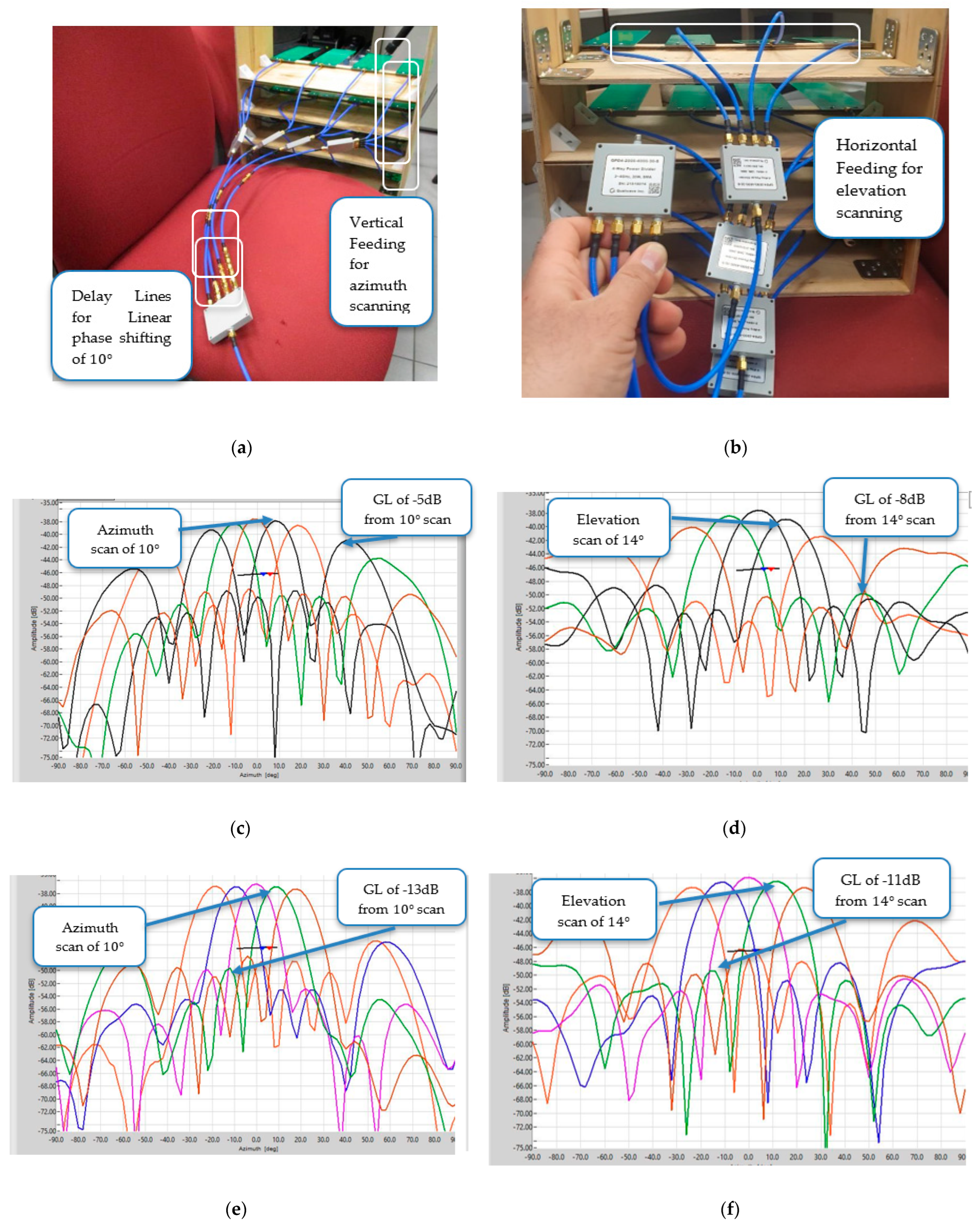
5.2. Dipole Array vs. Yagi–Uda Array Measurements with Scanning

Testing the above array over several frequencies and with azimuth/elevation scans, we obtained the bandwidth and spatial gain performances of five beams for the azimuth and elevation. The scans of 0 ° ,   ± 10 ° ,   ± 20 ° in the azimuth and 0 ° ,   ± 14 ° ,   ± 28 ° in elevation were implemented by linear phase shifting with delay lines and the constructing architecture of the vertical and horizontal feeding networks, as displayed in Figure 17a,b. The measured results displayed in Figure 17c,d show the impossibility of scanning with the dipole due to its low PSL—whereas scanning is possible with the Yagi–Uda array, as displayed in Figure 17e,f, as it meets the requirement of P S L > 10   d B , thanks to the element’s GL suppression.
In addition, the average measured gain of the directional array scanned beams is greater by 2.5 dB than that of the dipole array, as displayed in Figure 17e,f.

5.3. Efficiency

The losses in the system consisted of the PCB’s dielectric loss of 0.5 dB and 2 dB in the antenna. The matching loss (return loss) was negligible as the antenna was matched.
Comparing the evaluated directivity based on the measured gain with the theoretical directivity, we obtained the following efficiency results, in Table 6, for each antenna type for both the azimuth and elevation.
As we can see, the efficiency of the Yagi–Uda array was superior than that of the dipole array and corresponded to the results of the CST simulation, where the difference between the gain and the realized gain in Figure 15a was ~1 dB.

6. Discussion and Conclusions

In this paper, a design approach and the implementation of a super-directive antenna array was presented. This type of antenna is valuable in a restricted aperture scan for achieving a narrow antenna beam that increases the angular resolution and measurement precision of tracked targets and also enlarges the detection range or, alternatively, achieves the same performance with a lower number of elements-meeting the goal of low-cost production. The design of the directional array was based on the Yagi–Uda microstrip PCB and in both simulations and measurements showed a significant directivity improvement of ~ 2.5   d B in comparison to a dipole array with azimuth spacing of λ , as well as the possibility of scanning at ± 20 ° with no GL. Some applications for the super-directive antenna could be in radars for high-range performance, in wireless communication for high data rates, and also for wireless power transfer (WPT)-achieving high performance with much less power. Remarkable improvements were achieved in radars due to the scanning needs and the two-directional gains-both in the transmitter and receiving modes—which is equivalent to enlarging the radar maximum range by 33 % , the opportunity of the azimuth scan by 40 ° , and resulting in three times less power according to the radar equation.
The design working point of a phased array system, exploiting the benefits of this super directive antenna by both enlarging the scanning aperture and achieving higher gain, should take into account the tradeoff of the desired scan coverage and, consequently, choose the number of elements and optimized element places. The opportunity of choosing the appropriate design for meeting these requirements provides a larger degree of freedom, including in the number of elements, the element power, and unconventional element spacing that is larger than the classical d < λ 1 + | sin ( a z ) | . Moreover, this design’s architecture supports a combined module and antenna on a unified board thanks to the End-Fire radiation pattern and its low-cost manufacturing, which should be evaluated.
Superior super-directive results could probably be achieved using spacing of 2 λ and implementing a MIMO radar technique for generating a uniform grid array spaced at λ [30,31]. This virtual array was achieved using DBF [32] technology and equivalently duplicated the receivers, as shown in Figure 18, thanks to the significant reduction in undesired coupling, which strongly depends on spacing—as discussed and displayed in Figure 7. Such a design could achieve very high directivity in separated radar architecture [15], especially for FMCW in automotive car radars.
A challenge for the radar utilization of the super-directive concept in receiving mode is the GL presence in undesired directions. This can be solved by some processing techniques including tapering in transmission to improve the sidelobes, suppressing undesired clutter in the receiving mode with null. Other opportunities for utilizing this concept that should be examined include focusing energy in the near field using element phase optimization and using this design for implementing phased arrays in THz, which better exploits the sufficient needs of wider feed lines in comparison to patch antenna feed lines.

Author Contributions

B.L. wrote and performed the simulations; B.L. and E.L. carried out the LAB measurements; B.L. and Y.P. conceived the theory; B.L. and Y.P. wrote the paper. All authors have read and agreed to the published version of the manuscript.

Funding

This research received no external funding.

Data Availability Statement

All data included in this study are available upon request by contacting the corresponding author.

Conflicts of Interest

The authors declare no conflict of interest.

References

  1. Brookner, E. Developments and breakthroughs in radars and phased-arrays. In Proceedings of the 2016 IEEE Radar Conference (RadarConf), Philadelphia, PA, USA, 2–6 May 2016. [Google Scholar]
  2. Buttazzoni, G.; Babich, F.; Vatta, F.; Comisso, M. Geometrical synthesis of sparse antenna arrays using compressive sensing for 5G IoT applications. Sensors 2020, 20, 350. [Google Scholar] [CrossRef] [PubMed] [Green Version]
  3. Bocon, P.; McGree, T.; Renfro, J. Phased Array Performance Characteristics and Compliance with Satcom Military Standards. In Proceedings of the MILCOM 2005—2005 IEEE Military Communications Conference, Atlantic City, NJ, USA, 17–20 October 2005. [Google Scholar]
  4. Haupt, R. Phase-only adaptive nulling with a genetic algorithm. IEEE Trans. Antennas Propag. 1997, 45, 1009–1015. [Google Scholar] [CrossRef] [Green Version]
  5. Cheston, T.C.; Frank, J. Phased Array Radar Antennas. In Radar Handbook, 2nd ed.; Skolnik, M.I., Ed.; McGraw-Hill: Boston, MA, USA, 1990; pp. 7.1–7.36. [Google Scholar]
  6. Hansen, R.C. Basic Array Characteristics. In Phased Array Antennas, 2nd ed.; Chang, K., Ed.; WILEY: Hoboken, NJ, USA, 2009; pp. 7–40. [Google Scholar]
  7. Singh, H.; Sneha, H.L.; Jha, R.M. Mutual coupling in phased arrays: A review. Int. J. Antennas Propag. 2013, 2013, 348123. [Google Scholar] [CrossRef] [Green Version]
  8. Balanis, C.A. Arrays: Linear, planar, and circular. In Antenna Theory, 2nd ed.; John Wiley & Sons: New York, NY, USA, 1997; pp. 266–270. [Google Scholar]
  9. Baktır, Y. Investigation of Superdirective Antenna Arrays. Master’s Thesis, Middle East Technical University, Ankara, Turkey, 2009. [Google Scholar]
  10. Dawoud, M.; Hassan, M. Design of superdirective endfire antenna arrays. IEEE Trans. Antennas Propag. 1989, 37, 796–800. [Google Scholar] [CrossRef] [Green Version]
  11. Tai, C. The optimum directivity of uniformly spaced broadside arrays of dipoles. IRE Trans. Antennas Propag. 1964, 12, 447–454. [Google Scholar] [CrossRef]
  12. Eibert, T.F. Fundamentals of Antennas, Arrays, and Mobile Communications. In Antenna Engineering Handbook, 4th ed.; Volakis, J.L., Ed.; McGraw-Hill: New York, NY, USA, 2007; pp. 3–23. [Google Scholar]
  13. Haskou, A.; Sharaiha, A.; Collardey, S. Design of Small Parasitic Loaded Superdirective End-Fire Antenna Arrays. IEEE Trans. Antennas Propag. 2015, 63, 5456–5464. [Google Scholar] [CrossRef] [Green Version]
  14. Wideband Pattern Reconfigurable Printed-Yagi Antenna Array Based on Feed Structure. Available online: https://www.scielo.br/j/jmoea/a/xYZNm9pH7kxF6FBbshzPv8L/?format=html (accessed on 1 July 2022).
  15. Huizing, A.G. Scalable multifunction RF system: Combined vs. separate transmit and receive arrays. In Proceedings of the 2008 IEEE Radar Conference, Rome, Italy, 26–30 May 2008; pp. 1–6. [Google Scholar]
  16. Cohen, D.; Cohen, D.; Eldar, Y.C. High resolution FDMA MIMO radar. IEEE Trans. Aerosp. Electron. Syst. 2019, 56, 2806–2822. [Google Scholar] [CrossRef] [Green Version]
  17. Levanon, N. Radar Principles; John Wiley & Sons: New York, NY, USA, 1988; pp. 4–5. [Google Scholar]
  18. Kildal, P.S. Array antennas. In Foundation of antenna engineering; Kildal Antenn AB: Gothenburg, Swedan, 2015; pp. 346–348. [Google Scholar]
  19. Elliott, R.S. The Design of Feeding Structures for Antenna Elements and Arrays. In Antenna Theory and Design; John Wiley & Sons: Hoboken, NJ, USA, 2003; pp. 355–358. [Google Scholar]
  20. Chen, G.-Y.; Sun, J.-S. A printed dipole antenna with microstrip tapered balun. Microw. Opt. Technol. Lett. 2004, 40, 344–346. [Google Scholar] [CrossRef]
  21. Richards, M.A. Introduction to Radar Systems. In Fundamentals of Radar Signal Processing; McGraw-Hill Education: New York, NY, USA, 2005; p. 16. [Google Scholar]
  22. Collin, R.E. Antennas and Radiowave Propagation; McGraw Hill: New York, NY, USA, 1985. [Google Scholar]
  23. Kaschel, H.; Ahumada, C. Design of Rectangular Microstrip Patch Antenna for 2.4 GHz applied a WBAN. In Proceedings of the 2018 IEEE International Conference on Automation/XXIII Congress of the Chilean Association of Automatic Control (ICA-ACCA), Concepcion, Chile, 17–19 October 2018; pp. 1–6.1. [Google Scholar]
  24. Zucker, F.J. Fundamentals of Antennas, Surface-Wave Antennas. In Antenna Engineering Handbook, 4th ed.; Volakis, J.L., Ed.; McGraw-Hill: New York, NY, USA, 2007; pp. 10–14. [Google Scholar]
  25. Elliott, R.S. Linear array analysis. In Antenna Theory and Design; John Wiley & Sons: Hoboken, NJ, USA, 2003; p. 125. [Google Scholar]
  26. Wallace, R.; Dunbar, S. 2.4 GHz YAGI PCB Antenna; Texas Instrument Application Note DN034. Available online: https://www.ti.com.cn/cn/lit/an/swra350/swra350.pdf (accessed on 1 July 2022).
  27. Ertas, M.; Siva, A.; Dalkara, T.; Uzuner, N.; Dora, B.; Inan, L.; Idiman, F.; Sarica, Y.; Selçuki, D.; Oğuzhanoğlu, A.; et al. Validity and Reliability of the Turkish Migraine Disability Assessment (MIDAS) Questionnaire. Headache J. Head Face Pain 2004, 44, 786–793. [Google Scholar] [CrossRef] [PubMed]
  28. Elliott, R.S. Linear array: Synthesis. In Antenna Theory and Design; John Wiley & Sons: Hoboken, NJ, USA, 2003; p. 156. [Google Scholar]
  29. do Nascimento Silva, C.; de Melo, D.L.; de Oliveira, J.A.; da Silva, A.L.A.; de Oliveira, A.B.; Barboza, A.G.; do Nascimento, D.L.S.; de Filgueiras Gomes, D.; de Melo, M.T.; Kleinau, B.A.; et al. Analysis of a Linear Modified Yagi-Uda array using Particle Swarm Optimization for the Radiation Pattern Synthesis. In Proceedings of the 2021 IEEE International Conference on Microwaves, Antennas, Communications and Electronic Systems (COMCAS), Tel Aviv, Israel, 1–3 November 2021; pp. 395–400. [Google Scholar]
  30. Savy, L.; Lesturgie, M. Coupling effects in MIMO phased array. In Proceedings of the 2016 IEEE Radar Conference (Radar-Conf), Philadelphia, PA, USA, 2–6 May 2016; pp. 1–6. [Google Scholar]
  31. Chen, X.; Zhang, S.; Li, Q. A Review of Mutual Coupling in MIMO Systems. IEEE Access 2018, 6, 24706–24719. [Google Scholar] [CrossRef]
  32. Steyskal, H. Digital beamforming. In Proceedings of the 1988 18th European Microwave Conference, Stockholm, Sweden, 15 September 1988; pp. 49–57. [Google Scholar]
Figure 1. Element Array in the X–Z plane.
Electronics 11 02233 g001
Figure 2. (a) Flow chart of a super-directive array design; (b) Yagi–Uda element and AF with a 10 ° azimuth scan; (c) Azimuth array pattern based on a Yagi–Uda element with a 10° azimuth scan.
Electronics 11 02233 g002aElectronics 11 02233 g002b
Figure 3. (a) One-sided dipole antenna implementation fed by Phase Shifter and Splitter microwave components; (b) Top views of an antipodal dipole antenna without splitter and phase shifter components; (c) Bottom view of the antipodal dipole antenna including a rectangular ground.
Electronics 11 02233 g003aElectronics 11 02233 g003b
Figure 4. (a) Return Loss magnitude; (b) Far-Field 3D pattern of dipole antenna; (c) 2D Far-Field azimuth view; (d) 2D Far-Field elevation view.
Electronics 11 02233 g004
Figure 5. (a) Yagi–Uda element—Top view.; (b) Yagi–Uda element—Bottom view.
Electronics 11 02233 g005
Figure 6. (a) Return Loss; (b) Farfield plot of the Yagi–Uda antenna; (c) Elevation Farfield directivity (polar view); (d) Elevation Farfield directivity (cartesian view); (e) Azimuth Farfield directivity (polar view); (f) Azimuth Farfield directivity (cartesian view).
Electronics 11 02233 g006
Figure 7. (a) Coupling between two adjacent horizontal elements; (b) Coupling between two adjacent vertical elements; (c) Coupling between two adjacent horizontal elements in 2.4 GHz, d x = λ ; (d) Coupling between two adjacent vertical elements in 2.4 GHz, d z = 0.7 λ .
Electronics 11 02233 g007
Figure 8. (a) Farfield antenna measurement setup (b) Horizontal gain measurements of the Yagi–Uda and dipole element; (c) Elevation gain measurements of the Yagi–Uda and dipole element.
Electronics 11 02233 g008
Figure 9. Element Array in X–Z plane; A—Dipole Array with d x = 0.5 λ ; B—Yagi-Uda array with d x = 1 λ ; C—Yagi-Uda array with d x = 1.4 λ ; D—The super-directivity domain.
Electronics 11 02233 g009
Figure 10. (a) Azimuth AF and Element Pattern of a dipole array without scanning; (b) Azimuth Array Pattern of a dipole array without scanning; (c) Azimuth AF and Element Pattern of a dipole array with azimuth scans of 5 degrees; (d) Azimuth Array Pattern of a Yagi–Uda array with azimuth scans of 5 degrees.
Electronics 11 02233 g010
Figure 11. (a) Azimuth AF and Element Pattern of a Yagi–Uda array without scanning; (b) Azimuth Array Pattern of a Yagi–Uda array without scanning; (c) Azimuth AF and Element Pattern of a Yagi–Uda array with azimuth scans of 10 degrees; (d) Azimuth Array Pattern of a Yagi–Uda array with azimuth scans of 10 degrees; (e) Azimuth AF and Element Pattern of a Yagi–Uda array with azimuth scans of 15 degrees; (f) Azimuth Array Pattern of a Yagi–Uda array with azimuth scans of 15 degrees.
Electronics 11 02233 g011aElectronics 11 02233 g011b
Figure 12. (a) Array of a 4 × 4 dipole element; (b) Element pattern within an array of 4 × 4 dipole elements.
Electronics 11 02233 g012
Figure 13. (a) Array pattern of 4 × 4 dipole elements—Azimuth’s cartesian view; (b) Array pattern of 4 × 4 dipole elements—Elevation’s cartesian view.
Electronics 11 02233 g013aElectronics 11 02233 g013b
Figure 14. (a) Array of 4 × 4 Yagi–Uda elements—Top view; (b) Element pattern within an array of 4 × 4 Yagi-Uda elements—Back view; (c) Element pattern within an array of 4 × 4 Yagi-Uda elements—Front view; (d) Element pattern inside an array of 4 × 4 Yagi-Uda element—Top mesh view.
Electronics 11 02233 g014
Figure 15. (a) Array pattern of 4 × 4 Yagi–Uda elements—3D view (Gain, Realized gain); (b) Array pattern of 4 × 4 Yagi–Uda elements—Azimuth’s cartesian view; (c) Array pattern of 4 × 4 Yagi–Uda elements—Elevation’s cartesian view.
Electronics 11 02233 g015aElectronics 11 02233 g015bElectronics 11 02233 g015c
Figure 16. (a) Farfield antenna measurement setup; (b) Full 4 × 4 Yagi array; (c) Full 4 × 4 Yagi array; (d) Pattern 4 × 4 array of Yagi elements vs. dipole elements and reference antenna without scanning at 2.4 GHz.
Electronics 11 02233 g016
Figure 17. (a) Azimuth feed network setup; (b) Elevation feed network setup; (c) Azimuth gain of dipole array with azimuth scanning; (d) Elevation gain of dipole array with elevation scanning; (e) Azimuth gain of the Yagi–Uda array with azimuth scanning; (f) Elevation gain of the Yagi–Uda array with elevation scanning; (g) Azimuth gain comparison of the Yagi–Uda and dipole arrays at 2.3 GHz with scanning; (h) Azimuth gain comparison of the Yagi–Uda and dipole arrays at 2.45 GHz with scanning.
Electronics 11 02233 g017aElectronics 11 02233 g017b
Figure 18. Separated radar with MIMO DBF virtual array duplication.
Electronics 11 02233 g018
Table 1. System Design Requirement.
DenotationSymbolValue
Operating frequency fo2.4 GHz
Beamwidth Az/ElBWAz = 12.5 deg; El = 18 deg;
Scan aperture θ <40 deg
DirectivityD20 dB
BandwidthB200 MHz
Side lobe levelSLL<−10 dB
Element number in AzimuthNx4
Element number in ElevationNz4
Table 2. Element Design Requirement.
DenotationSymbolValue
Operating frequency fo2.4 GHz
Dielectric substrate ϵ r FR4—4.3
Thickness t0.035 mm
Height of the dielectric substrateh_sub1 mm
Return lossS11<−15 dB
Impedance of the antennadipole73 Ohms
DirectivityD9
BeamwidthBW60 deg
Table 3. Dipole results.
DenotationSymbolValue
50 ohms transition Line lengthL_50_ohms5 mm
50 ohms transition Line widthW_50_ohms1.9 mm
Rectangular ground widthW_ground35 mm
Quarter wave transformer lengthL_quarter24.25 mm
Quarter wave transformer widthW_quarter0.6 mm
Dipole widthW_driver0.6 mm
Half Dipole lengthL_driver25.77 mm
Table 4. Yagi–Uda Results.
ParameterSymbolValue
50 ohms transition line lengthL_50_ohms5 mm
50 ohms transition line widthW_50_ohms1.9 mm
Rectangular ground widthW_ground35 mm
Quarter wave transformer lengthL_quarter26 mm
Quarter wave transformer widthW_quarter0.8 mm
Dipole widthW_driver0.8 mm
Half dipole lengthL_driver25.8 mm
Substrate widthW_sub60 mm
Substrate lengthL_sub120 mm
Director widthW_director0.6 mm
Director widthL_director39
Director distanceD_directors27
Number of directors#Directors3
Table 5. Yagi–Uda coupling measurements between adjacent elements (S12) in the vertical and horizontal positions.
Element’s DistanceVerticalHorizontal
0.58 λ −18 dB−22 dB
0.67 λ −19 dB−23 dB
0.75 λ −21 dB−24 dB
0.83 λ −23 dB−26 dB
0.92 λ −26 dB−29 dB
1.00 λ −26 dB−31 dB
1.50 λ −34 dB−44 dB
Table 6. Array efficiencies.
Antenna TypeAz/ElMeasured
Gain
Measured Directivity (Gain + Loss)D0 = 4πA/λ²η Aperture
DipoleAzimuth15.5 dBi17.5 dBi20.3 dBi−3 dB
DipoleElevation15 dBi17 dBi20.3 dBi−3.3 dB
Yagi–UdaAzimuth17.3 dB19.3 dBi20.1 dBi−0.8 dB
Yagi–UdaElevation17.3 dB19.3 dBi20.1 dBi−0.8 dB
Publisher’s Note: MDPI stays neutral with regard to jurisdictional claims in published maps and institutional affiliations.

