Article

Ultra-Low-Cost Design of Ripple Carry Adder to Design Nanoelectronics in QCA Nanotechnology

1
Department of Electrical Engineering, Islamic Azad University of Science and Research Tehran (Kerman) Branch, Kerman 7718184483, Iran
2
Department of Information and Communication Technology (ICT), Mawlana Bhashani Science and Technology University, Tangail 1902, Bangladesh
3
Department of Electrical and Computer Engineering, University of Saskatchewan, Saskatoon, SK S7N 5A9, Canada
4
Facultad de Ingeniería y Ciencias, Universidad Adolfo Ibáñez, Diagonal Las Torres 2640, Peñalolén, Santiago 7941169, Chile
5
Department of Civil, Environmental and Natural Resources Engineering, Lulea University of Technology, SE 971 87 Lulea, Sweden
6
RIKEN Center for Advanced Photonics, RIKEN, Wako 351-0198, Saitama, Japan
*
Authors to whom correspondence should be addressed.
Electronics 2022, 11(15), 2320; https://doi.org/10.3390/electronics11152320
Submission received: 29 June 2022 / Revised: 19 July 2022 / Accepted: 22 July 2022 / Published: 26 July 2022
(This article belongs to the Special Issue Resource Sustainability for Energy and Electronics)

Abstract

:
Due to the development of integrated circuits and the lack of responsiveness to existing technology, researchers are looking for an alternative technology. Quantum-dot cellular automata (QCA) technology is one of the promising alternatives due to its higher switch speed, lower power dissipation, and higher device density. One of the most important and widely used circuits in digital logic calculations is the full adder (FA) circuit, which actually creates the problem of finding its optimal design and increasing performance. In this paper, we designed and implemented two new FA circuits in QCA technology and then implemented ripple carry adder (RCA) circuits. The proposed FAs and RCAs showed excellent performance in terms of QCA evaluation parameters, especially in cost and cost function, compared to the other reported designs. The proposed adders’ approach was 46.43% more efficient than the best-known design, and the reason for this superiority was due to the coplanar form, without crossovers and inverter gates in the designs.

1. Introduction

As the advancement and development of integrated circuits progressed day by day and the lack of response of the complementary metal–oxide–semiconductor (CMOS) technology due to the problems at the nanoscale, new technologies at the nanoscale were introduced. These were technologies such as: carbon nanotubes, quantum-dot cellular automata (QCA), nanomagnetic logic, resonant tunneling diodes, and spin-wave devices. One of the most promising alternatives to replace CMOS technology is QCA technology. It is due to the extraordinary features and benefits of QCA, which are high switch speed, an operating frequency in the terahertz frequency range, very low power dissipation, extremely high device density, and implementation at the level of atoms and molecules.
To implement bistable and local QCA paradigm interactions, several different implementations have been proposed, such as atoms, molecules, and semiconductors that have been studied based upon electrostatic interactions [1]. In addition, various experimental devices [2,3] have been developed and successfully tested [2,3]. There are four types of QCA. Molecular and magnetic QCA are operable at room temperature while metal and semiconductor QCA operate at around cryogenic temperatures.
Furthermore, several typical clock schemes have been proposed for QCA circuits to realize the specifications of standard units and develop routing and placement algorithms [4,5]. All the concepts presented in this paper were based on a QCA semiconductor. Adders are one of the main building blocks of many VLSI systems, such as microprocessors and various processors. One of the most important and widely used circuits in mathematical computations of digital logic is the full adder (FA) circuit; the optimal design and performance improvement of this circuit has special importance. Improvements to this circuit will result in improved and optimized performance for more complex circuits [6,7]. Moreover, cost-effective and efficient design of FA and RCA circuits can achieve more efficient and cost-effective complex circuits.
Therefore, in the present article, two designs and implementations of this circuit were presented. To show the performance improvement, we implemented and applied these FA designs in designing and implementing the RCA circuits. This article is composed as follows: Section 2 presents the background of QCA and an overview of previous works. The design, implementation, and simulation results of the proposed FA and RCA circuits are presented in Section 3. Tables and diagrams for comparison and evaluation of important QCA parameters are presented in Section 4, the energy dissipation analysis in Section 5, and the conclusions of this article are presented in Section 6.

2. QCA Basics

2.1. The QCA Cells Basics

Similar to transistors in CMOS circuits, QCA cells serve as the primary units of the QCA circuits for the design and development of computing and communication devices. Each QCA cell is composed of four holes (quantum dots) and two electrons are trapped inside it (Figure 1a). Because of the Columbic effects, the electrons are always in a position where there is the minimal potential energy, and the electrons are placed diagonally inside the holes. By placing the electrons diagonally, two logical structures “0” and “1” (polarizations −1 and +1, respectively) are created [8,9], as shown in Figure 1b.
Four-phase clocks are also used as clocking in the QCA design to reduce the signal metastability and ensure the correct propagation of signals in the circuit [9] (Figure 2).
QCA wire is used to communicate between gates, blocks, and QCA circuits, and it is created by placing the QCA cells next to each other [8,10]. The majority gate (MV) is one of the most widely used gates in the design of the QCA circuits and is among the basic gates of this technology. The MV has the number of individual inputs and one output that the majority votes of the inputs determine the amount (value) of the output. One of the most widely used MV gates in the design of the QCA circuits is the three-input MV gate, whose two examples are given in Figure 3, and in the proposed designs, we used both types [8,11] separately.

2.2. Overview of FA/RCA Designs

The design of the full adder circuit is of special importance due to its many usages. In QCA technology, due to the high capability and implementation of composite gates, using majority gates and XOR gates independently and without using base gates (NOT gates, AND gates and OR gates) has caused this block (FA circuit) to be implemented without using base gates. This has led to the optimization and improvement of the main and basic parameters of QCA technology, including the number of cells, the occupied area, latency, and finally the implementation cost. For this reason, the implementation of composite and complex circuits using independent XOR gates (without the use of base gates in the implementation), improves the main QCA parameters and ultimately reduces the implementation cost and cost function. Thus, various designs and implementations for the FA circuit have been introduced. They have been introduced in multi-layer designs [12,13,14,15] with a high cost of implementation while some others are coplanar [16,17,18] which use rotational cells in the implementation; we do not consider these in this work due to their high cost of implementation and low sustainability. Some others [19,20,21] were coplanar and the implemented crossovers were based on the QCA’s clocking. This type of design also has a higher cost function due to the use of crossovers and inverter gates and not moving toward design and implementation without crossovers and inverter gates. As a result, in this paper, we proposed the FA design in a coplanar manner without the 45 cells, inverter gates, and crossovers. The design and implementation of FAs and RCAs are the first to be presented without the use of inverter gates in the implementation. However, all the proposed designs in this article and the QCA circuit parameters, such as cell number, the occupied area, latency, and cost function, were superior to previous works.

3. The Proposed Circuits

Adder blocks are one of the most important computational circuits, and they are used as the most applied arithmetic blocks. Among adder blocks, the FA block is one of the most common and principal computational blocks. In most FA circuit designs with QCA technology, the majority and inverter gates are prevalently used. In this work, the proposed FA and 4-bit RCA designs were implemented using the XOR gate while a nothing inverter gate (NOT gates) and a crossover were used to implement the proposed designs. Such designs and implementations are very important because it can achieve a lower cost function and ultimately lead to lower implementation costs than other designs.

3.1. The FA Circuit Design and Implementation

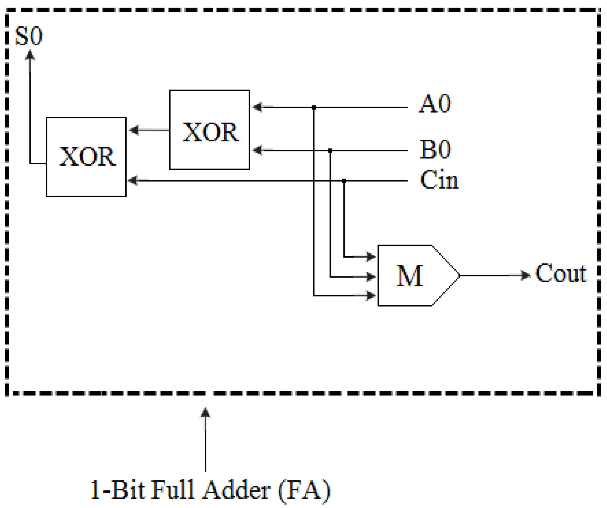
One of the most important and applied circuits and computing blocks of digital logic is the full adder (FA) circuit because this block is the main component of more complex circuits and computational systems. Improving and optimizing the performance of this circuit will improve and optimize larger and more complex circuits. Therefore, we designed and implemented two novel FA circuits with the “implementation with XOR gate” designed method. All of these designs were coplanar (single layer), and nowhere in these designs were inverter gates and crossovers not used. The Schematic logic diagram of these designs is shown in Figure 4.
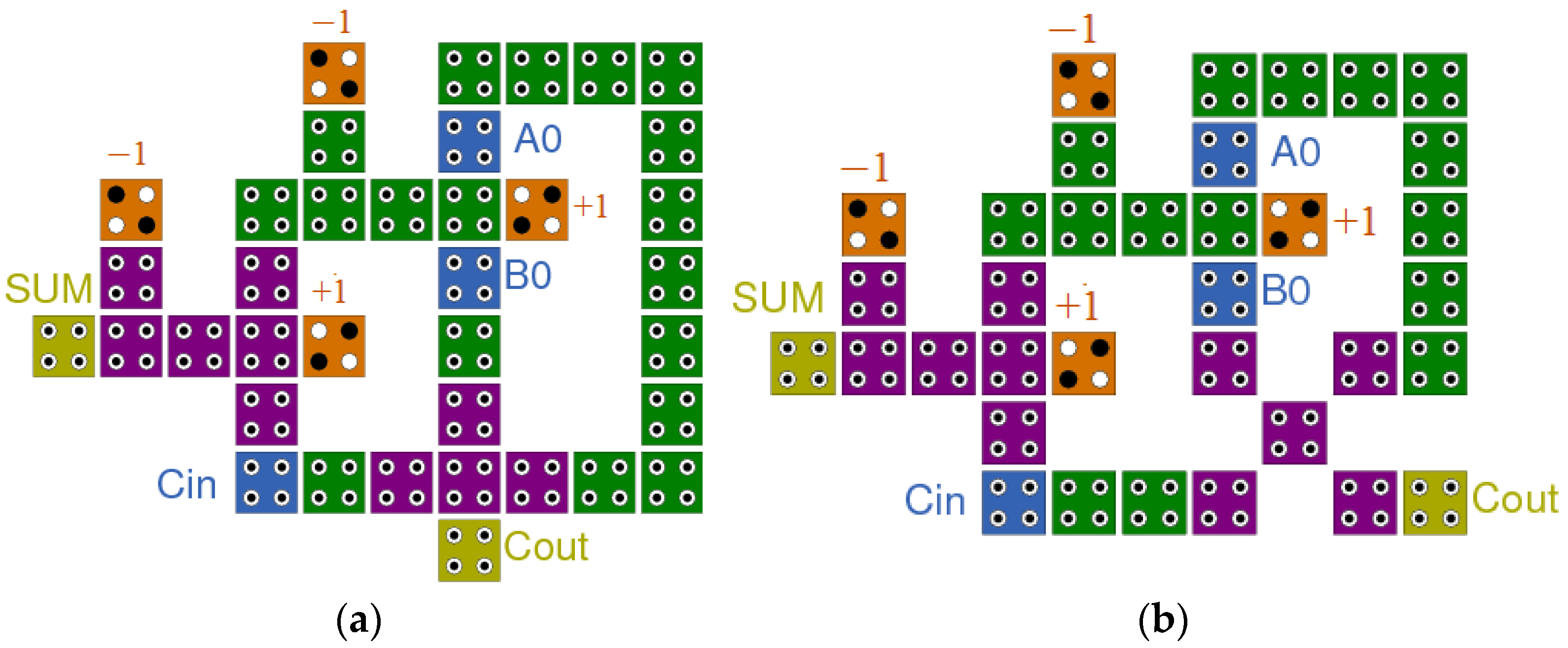
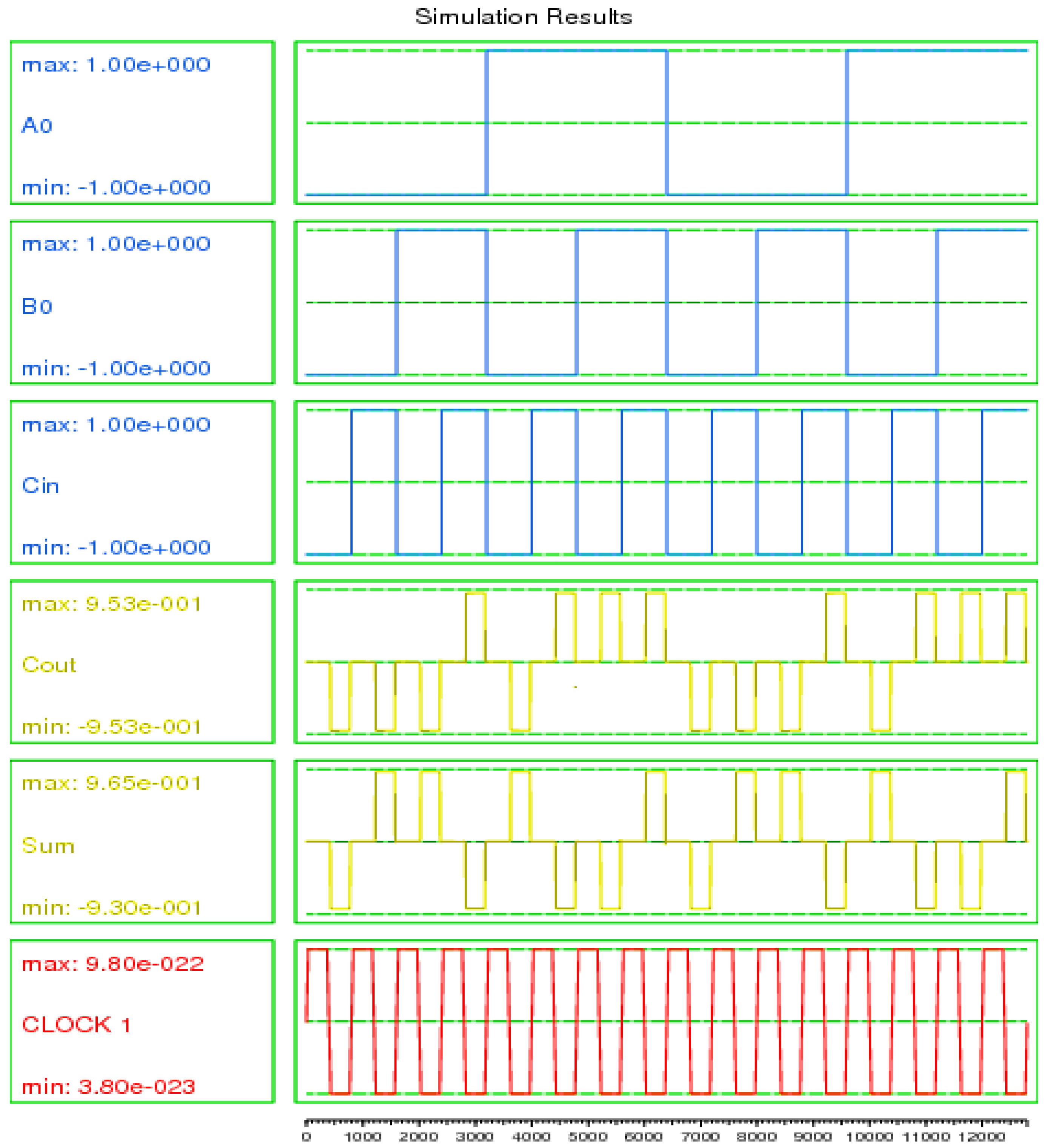
Figure 5a shows the implementation of the proposed (a) FA circuit. A0, B0 and Cin are the input cells, and Sum and Cout are the output cells of this design. This circuit contains 37 normal cells, 0.5 cycle latency, and a 0.031 µm2 occupied area. Figure 5b also shows the implementation of the proposed (b) FA circuit. This circuit also contains 35 normal cells, 0.5 cycle latency, and a 0.027 µm2 occupied area. As shown in Figure 5, the difference between the two proposed FAs (a and b) is in their majority gate (MV) that gives the Cout output. The proposed FA circuit (a) is based on a regular MV and the proposed FA (b) is based on an inverted MV. Since the latency of both outputs (Cout and SUM) are similar for both the proposed FA circuits, they give similar simulation outputs. Therefore, for the sake of brevity, we provided only one of the simulation results in exchange for similar inputs. Figure 6 shows the simulated output of these circuits. The evaluation of our proposed FA circuits in this research in comparison with previous works is given in Section 4. All the proposed designs of this research were significantly superior to all previous designs in terms of basic QCA parameters, such as cell number, the occupied area, and latency.

3.2. The RCA Circuit Design and Implementation

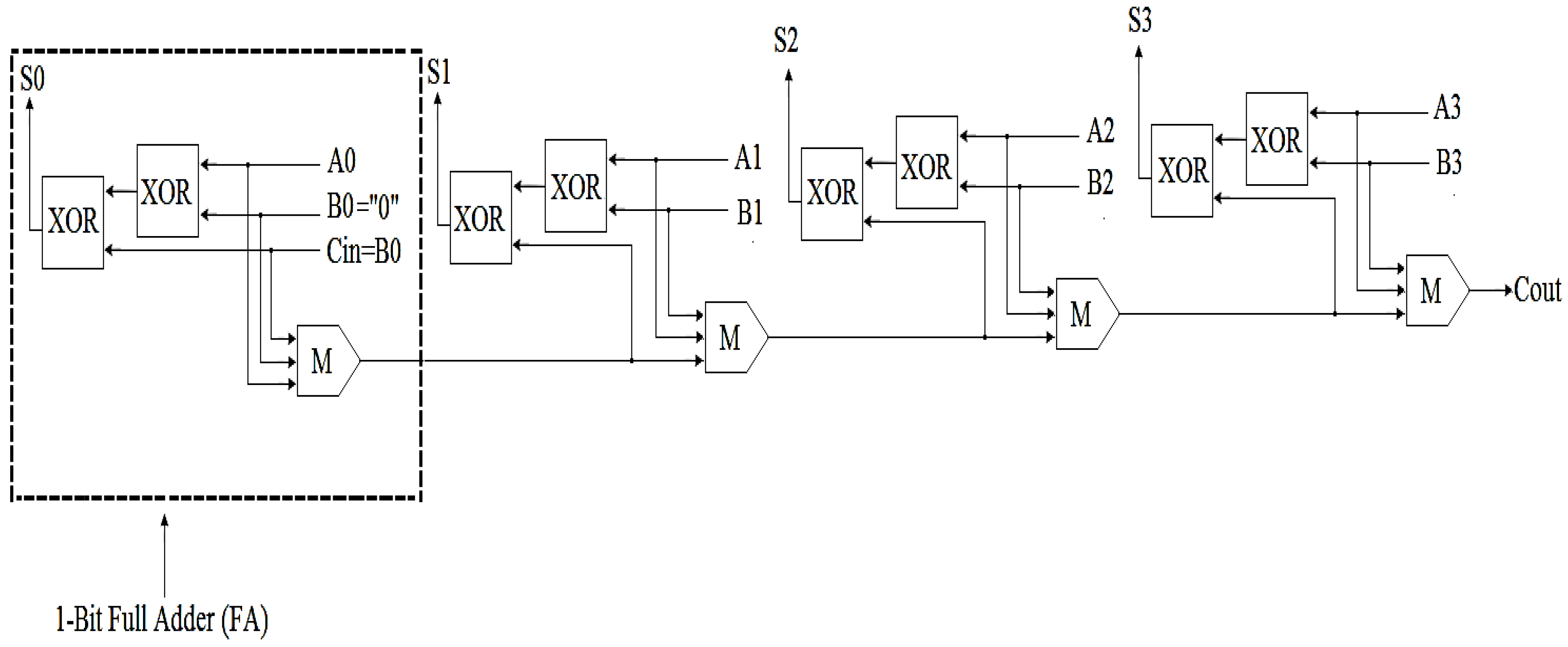
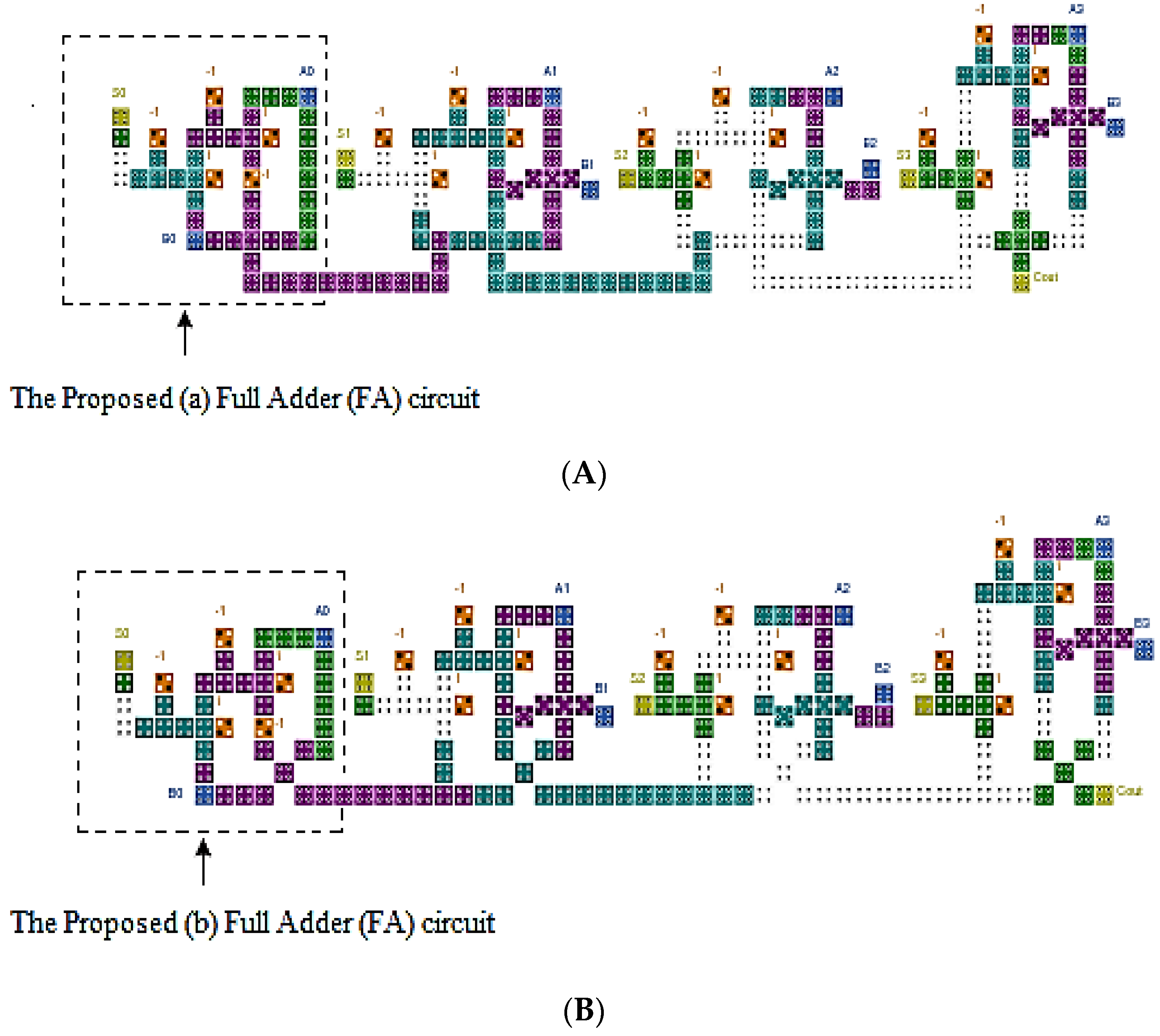
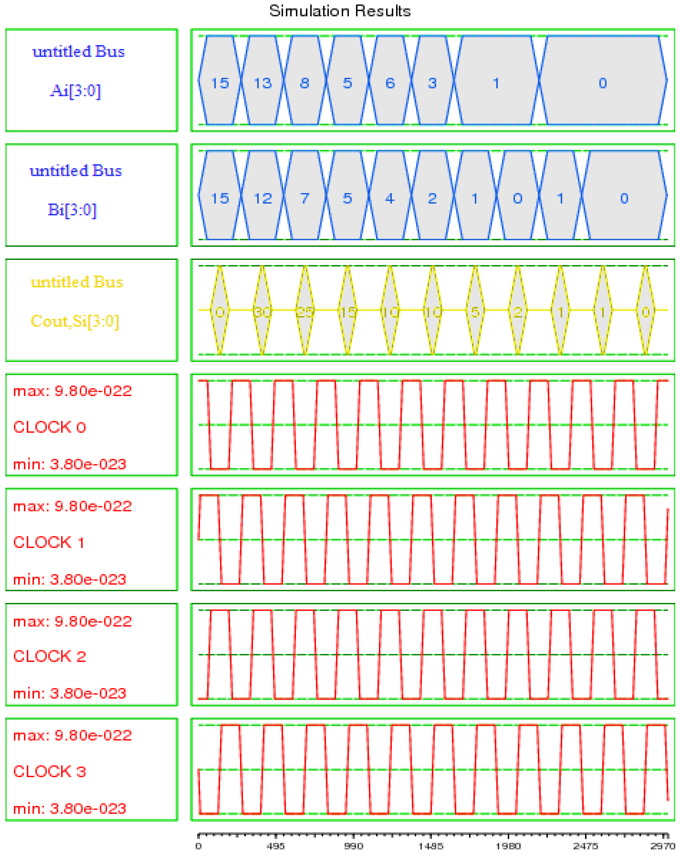
In this section, we designed two 4-bit RCA circuits using each of the proposed FA designs in the previous section. All these designs were coplanar (single layer). The block diagram of the two proposed 4-bit RCA designs is shown in Figure 7. Shown in this figure is a 4-bit adder using four full adders. This adder design is referred to as “ripple carry” since the carry ripples from one FA to another. As can be seen, A3, A2, A1, and A0 (untitled Bus A); B3, B2, B1, and B0 (untitled Bus B); and Cin are the input cells; and Cout, S3, S2, S1, and S0 (untitled Bus Sum) are the output cells in this block diagram. As a result, by using the two implementation hardware designs in Figure 5 and based on the block diagram of Figure 7, it is possible to achieve the two-implementation hardware of the 4-bit ripple carry adder circuit. Figure 8A shows the design and implementation of the proposed (A) 4-bit RCA circuit. This implementation includes 233 normal cells, 1.25 cycle latency, and 0.28 µm2 of the occupied area. Figure 8B also shows the design and implementation of the proposed (B) 4-bit RCA circuit, which includes 209 normal cells, 1.25 cycle latency, and a 0.25 µm2 occupied area. The difference between the two proposed 4-bit RCAs (A and B) is in their using MV gates. The proposed 4-bit RCA circuit (A) is based on a regular MV while the proposed 4-bit RCA (B) is based on an inverted MV. Since the latency of both outputs are similar for the both proposed 4-bit RCA circuits, they give similar simulation outputs. Therefore, for the sake of brevity, we provided only one of them in exchange for similar inputs. Figure 9 also shows the output of the simulation of these two proposed 4-bit RCA circuits.

4. Performance Evaluation

In this part, a comparative evaluation and analysis of the proposed 4-bit RCA circuits with previous works are given. For this evaluation, the number of cells, area, and latency of the proposed circuits are simulated with the QCA designer tool. We used QCADesiner 2.0.3 version and verified our designs by the Bistable Approximation and Coherence Vector simulation engine. Table 1 lists a brief description of the coherence vector simulation parameters used by the QCA Designer tool. The simulation results of the proposed FAs and 4-bit RCAs circuits of this research are also given in Table 2 and Table 3, respectively. One of the most important evaluation criteria for QCA circuits is cost function as reported in literature [22]. Equation (1) shows this evaluation criterion. Cost function is a composite measure, consisting of certain criteria that M indicates the number of majority gates, I the number of inverter gates, C the number of crossovers, and T also indicates the amount of output latency. The coefficients L, K, and P are also determined based on the importance of power dissipation, the occupied area, complexity, and latency, respectively. As shown in Table 3, our proposed adders (i.e., Proposed (A) and Proposed (B)) have a better advantage than the previous paradigms due to less use of the MV numbers. The reduction of the cost function is about 46.43% and 60.23% in comparison to [19,23], respectively. Moreover, the complexity is reduced by about 25% and 12.5% in comparison to [19,23], respectively, and the delay is about 28.57% and 54.55% in comparison to [19,23], respectively.
Cost Function = (MK + I + CL) × TP, 1 ≤ K, L, P
CostArea-Delay = A × TP, 0 ≤ p ≤ 2
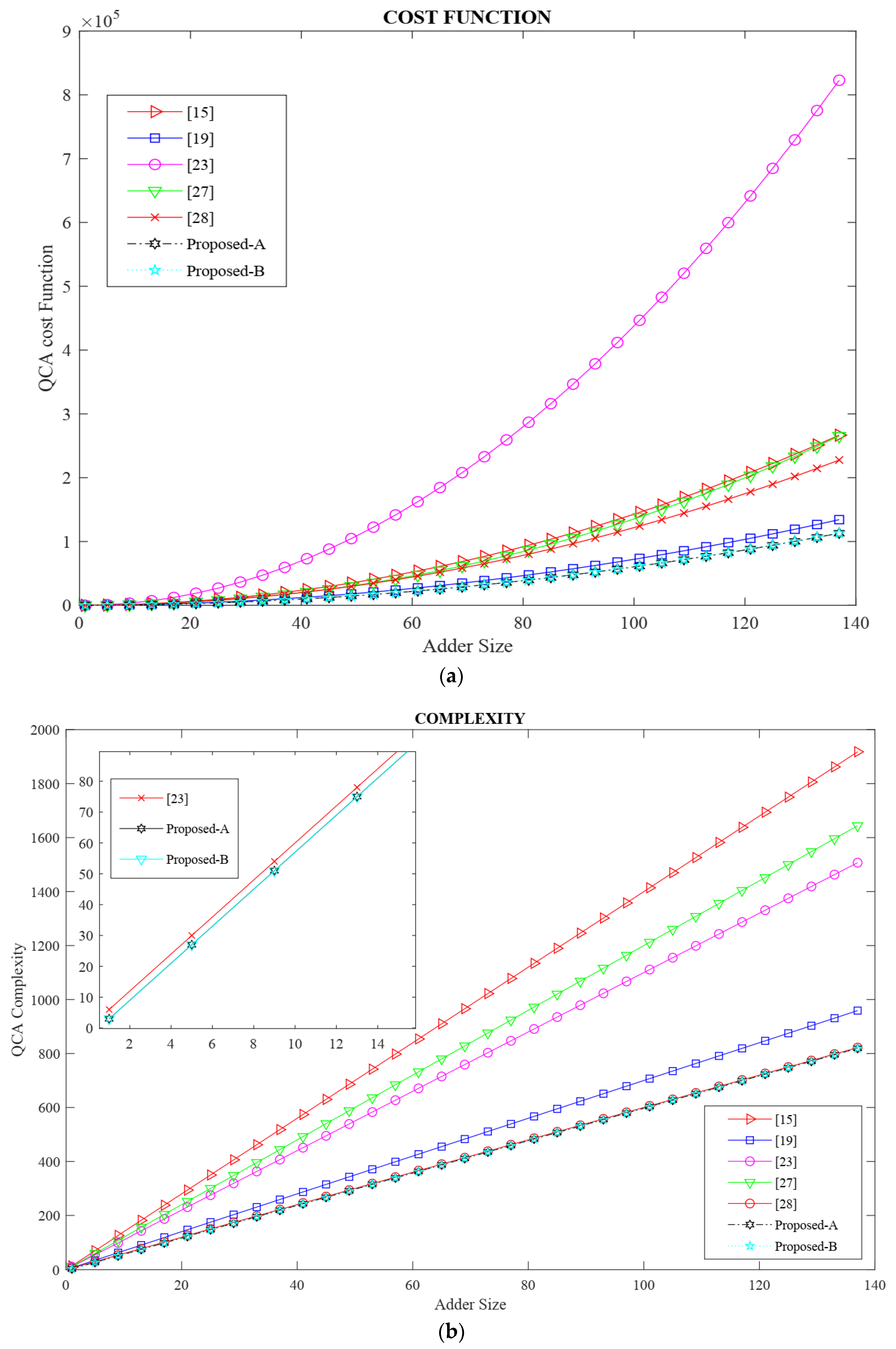
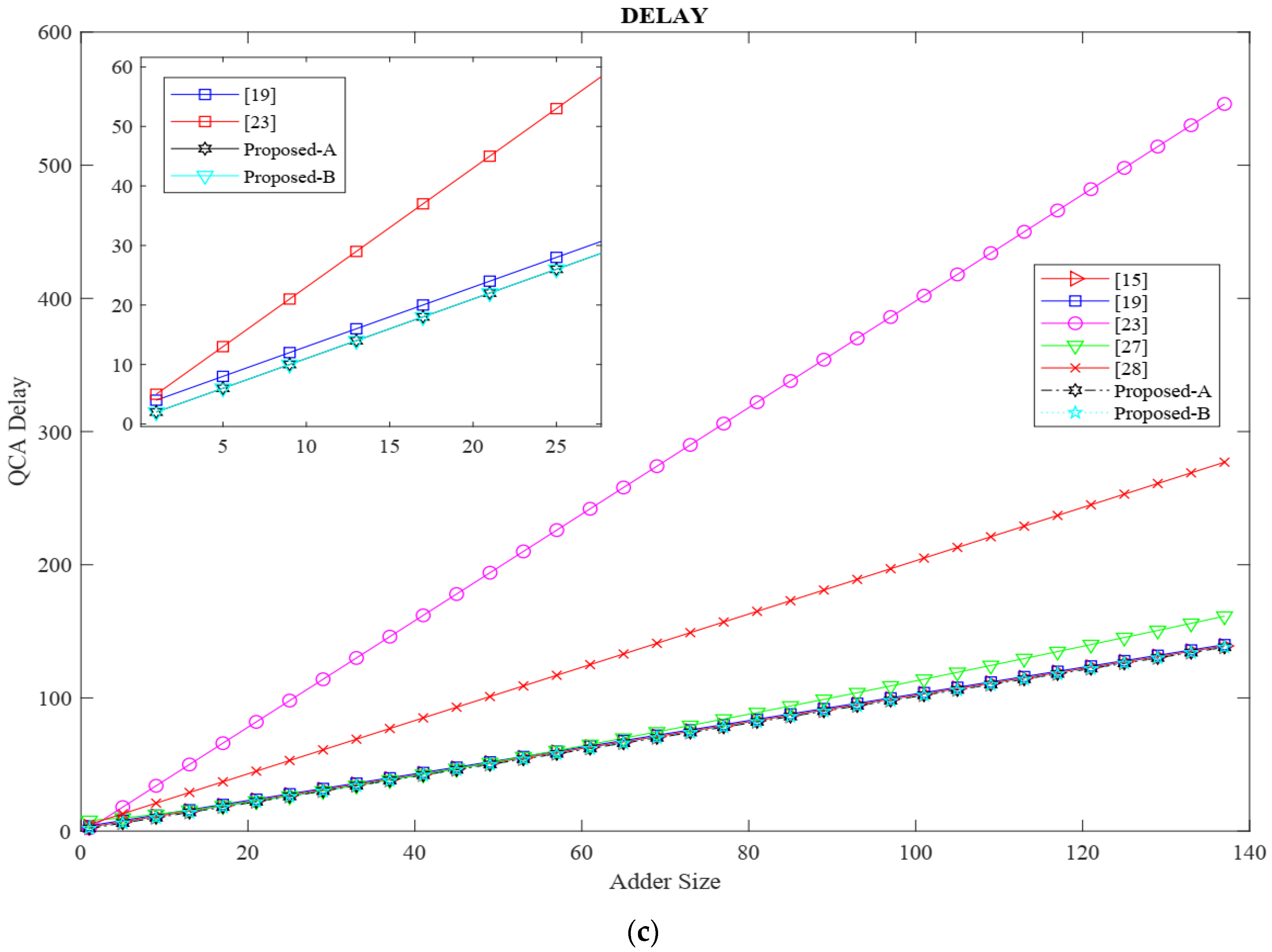
As shown in Table 3, the coefficients of K, L, P are considered equal to one (K, L, P = 1). To evaluate the performance of the novel RCAs in comparison with the performance of the previous paradigms, this evaluation has been performed. Figure 10a shows the evaluation and comparison of the cost function criterion at K, L, P = 1. The cost function of our proposed designs is significantly superior to all previous designs. The reasons for this superiority are due to the absence of the inverter gates, a crossover, and also fewer MV gates used in the implementation of our proposed designs. These comparisons and evaluations were performed in a size range of 1 ≤ n ≤ 128. Another evaluation was performed by using Equation (2) where A represents the occupied area and T represents the latency [22]. Figure 10b shows the comparison diagram of the complexity criterion, and it indicates our proposed designs in this research are superior to all previous works due to the less occupied area and less delay. In this comparison, the number of MV gates, the number of NOT gates, and the number of crossovers were considered, assuming that the cost of multi-layer crossovers is three times that of a coplanar (single layer) [22]. To measure the complexity of the novel proposed RCAs (n-bit) against previous designs, this evaluation was performed in the range of 1 ≤ n ≤ 128. As shown in Figure 11 for the review of this evaluation parameter, in this evaluation criterion, our proposed RCAs designs are significantly superior to all previous paradigms. Figure 10c also shows the delay criterion in order to measure the speed of QCA Adders. This comparison was also performed in the range of 1 ≤ n ≤ 128, and the fastest QCA Adder is related to our proposed designs, which are coplanar. As a result, in this evaluation criterion, our proposed QCA Adders designs are also superior to previous designs.

5. Energy Dissipation Analysis

One of the important parameters for evaluating performance and efficiency in the design of electronic devices is energy dissipation. The high-power estimation method [29] is the most common method for power approximation. In this section, a power dissipation analysis was performed using QCAPro tool [30]. In the calculations, the power consumption of all QCA cells is assumed to be the same amount. Therefore, the equation for instantaneous power is given by:
P t o t a l = d E d t = 2 [ d Γ d t λ ] + 2 [ Γ d λ d t ]
where λ the coherence vector and Γ is the state energy vector. The vector λ indicates the current state of a cell and the vector Γ signifies the steady state of the cell. The total energy dissipation in a time period [−t, t] and was estimated as follows:
E d i s s = 2 t t Γ d λ d t = 2 ( [ Γ λ ] t t t t λ d Γ d t d t )
and the power dissipation model can be estimated as follows:
P d i s s = E d i s s T c 2 T c Γ + × [ Γ | Γ | tanh ( | Γ | k B T ) Γ + | Γ + | tanh ( | Γ + | k B T ) ]
Using the value of clock low and high energies, the average leakage and switching power can be expressed as follows:
P a v g l e a k = 1 2 r i   =   r + 1 N p i , n m l e a k
P a v g s w i t c h = 1 2 r i   =   r + 1 N p i , n m s w i t c h
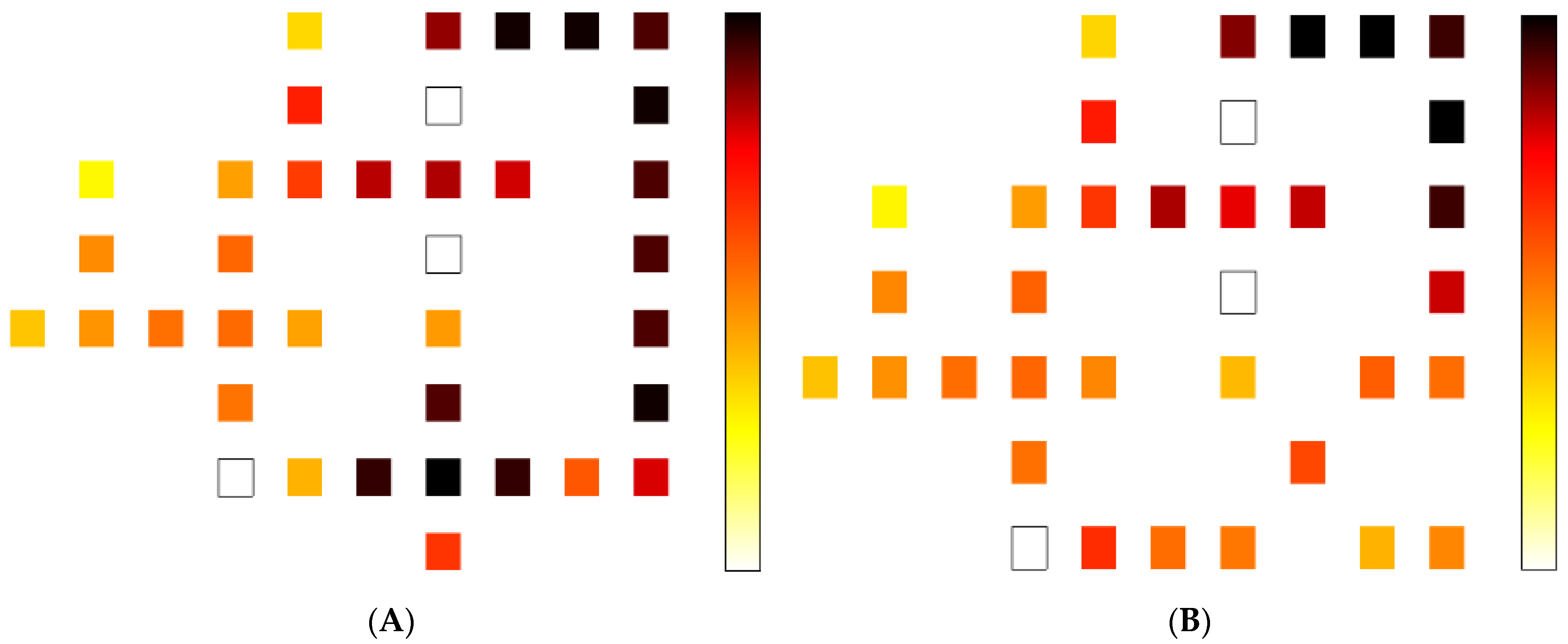
Table 4 shows the energy dissipation data of different multipliers at the 0.5 Ek, 1.0 Ek, and 1.5 Ek tunneling energy for the novel proposed FAs circuits. As shown in Table 4, for the proposed full adder A (FA-1), the energy dissipates are 60.22, 75.74, and 94.99 meV at 0.5, 1.0, and 1.5 Ek, respectively, while for the proposed full adder B (FA-2), the energy dissipates are 49.79, 65.67, and 84.81 meV at 0.5, 1.0, and 1.5 Ek, respectively. Figure 11 shows the thermal hotspots of our proposed full adders (FA-1 and FA-2) at 0.5 Ek where the dark cells indicate higher energy dissipated cells.

6. Conclusions

Many of the RCA designs in QCA technology were implemented with multi-layers but using rotational cells (45° cells). Furthermore, designing coplanar crossovers with adjacent clock phases in large designs increased latency. For these reasons, we used the minimum crossovers and 45° cells (rotational cells) in our designs. This led to the efficient RCA design of our proposed designs because they were designed as a coplanar (single layer) and with the minimum number of NOT gates, crossovers, and rotational cells. This made the implemented circuit more stable and robust than previous designs and also significantly superior to previous designs in terms of basic parameters, the number of cells, the occupied area, latency, cost function and cost area-delay. We used the proposed FA in 4-, 8-, 16-, 32-, 64-, and 128-bit ripple carry QCA adder. Due to the comparison and evaluation of the cost function parameter, the cost of implementing the n-bit RCA of our proposed designs was much lower. The proposed design was 46.43% more efficient in cost function than the best-known design [19] and the reasons for this were due to our innovative and creative design in using the minimum crossovers and inverter gates in the designs. The results showed that the proposed design was more efficient and cost-effective than the existing designs. Therefore, they can be used effectively in the design of more complex circuits and systems and improve and optimize composite and complex circuits.

Author Contributions

Conceptualization, M.V.; methodology, M.V.; validation, M.V. and A.N.B.; formal analysis, M.V.; investigation, M.V. and A.N.B.; writing—original draft preparation, M.V.; writing—review and editing, A.N.B., A.O. and K.A.W.; supervision, A.N.B., A.O. and K.A.W. All authors have read and agreed to the published version of the manuscript.

Funding

This research received no external funding.

Institutional Review Board Statement

Not applicable.

Informed Consent Statement

Not applicable.

Data Availability Statement

Data are contained within the article.

Conflicts of Interest

The authors declare no conflict of interest.

References

  1. Wang, L.; Xie, G. A Novel XOR/XNOR Structure for Modular Design of QCA Circuits. IEEE Trans. Circuits Syst. II Express Briefs 2020, 67, 3327–3331. [Google Scholar] [CrossRef]
  2. Snider, E.G.; Orlov, A.O.; Amlani, I.; Zuo, X.; Bernstein, G.H.; Lent, C.S.; Merz, J.L.; Porod, W. Quantum-dot cellular automata: Review and recent experiments (invited). J. Appl. Phys. 1999, 85, 4283–4285. [Google Scholar] [CrossRef]
  3. Macucci, M.; Gattobigio, M.; Bonci, L.; Iannaccone, G.; Prins, F.; Single, C.; Wetekam, G.; Kern, D. A QCA cell in silicon-on-insulator technology: Theory and experiment. Superlattices Microstruct. 2003, 34, 205–211. [Google Scholar] [CrossRef]
  4. Edrisi Arani, I.; Rezai, A. Novel circuit design of serial–parallel multiplier in quantum-dot cellular automata technology. J. Comput. Electron. 2018, 17, 1771–1779. [Google Scholar] [CrossRef]
  5. Vankamamidi, V.; Ottavi, M.; Lombardi, F. Two-dimensional schemes for clocking/timing of QCA circuits. IEEE Trans. Comput.-Aided Des. Integr. Circuits Syst. 2007, 27, 34–44. [Google Scholar] [CrossRef]
  6. Vahabi, M.; Lyakhov, P.; Bahar, A.N. Design and Implementation of Novel Efficient Full Adder/Subtractor Circuits Based on Quantum-Dot Cellular Automata Technology. Appl. Sci. 2021, 11, 8717. [Google Scholar] [CrossRef]
  7. Bhargav, A.; Huynh, P. Design and Analysis of Low-Power and High Speed Approximate Adders Using CNFETs. Sensors 2021, 21, 8203. [Google Scholar] [CrossRef]
  8. Vahabi, M.; Lyakhov, P.; Bahar, A.N.; Wahid, K.A. Design and Implementation of New Coplanar FA Circuits without NOT Gate and Based on Quantum-Dot Cellular Automata Technology. Appl. Sci. 2021, 11, 12157. [Google Scholar] [CrossRef]
  9. Tougaw, P.D.; Lent, C.S. Logical devices implemented using quantum cellular automata. J. Appl. Phys. 1994, 75, 1818–1825. [Google Scholar] [CrossRef]
  10. Kim, H.-I.; Jeon, J.-C. Quantum LFSR Structure for Random Number Generation Using QCA Multilayered Shift Register for Cryptographic Purposes. Sensors 2022, 22, 3541. [Google Scholar] [CrossRef]
  11. Lent, C.S.; Tougaw, P.D.; Porod, W. Quantum cellular automata: The physics of computing with arrays of quantum dot molecules. In Proceedings of the PhysComp 94: Workshop on Physics and Computing, Dallas, TX, USA, 17–20 November 1994; pp. 5–13. [Google Scholar]
  12. Cho, H.; Swartzlander, E.E. Adder and multiplier design in quantum-dot cellular automata. IEEE Trans. Comput. 2009, 58, 721–727. [Google Scholar] [CrossRef]
  13. Pudi, V.; Sridharan, K. Low Complexity Design of Ripple Carry and Brent–Kung Adders in QCA. IEEE Trans. Nanotechnol. 2011, 11, 105–119. [Google Scholar] [CrossRef]
  14. Hayati, M.; Rezaei, A. Design of novel efficient adder and subtractor for quantum-dot cellular automata. Int. J. Circuit Theory Appl. 2014, 43, 1446–1454. [Google Scholar] [CrossRef]
  15. Mohammadi, M.; Mohammadi, M.; Gorgin, S. An efficient design of full adder in quantum-dot cellular automata (QCA) technology. Microelectron. J. 2016, 50, 35–43. [Google Scholar] [CrossRef]
  16. Hanninen, I.; Takala, J. Robust adders based on quantum-dot cellular automata. In Proceedings of the 2007 IEEE International Conference on Application-Specific Systems, Architectures and Processors (ASAP), Montreal, QU, Canada, 9–11 July 2007. [Google Scholar]
  17. Ahmad, F.; Bhat, G.M.; Khademolhosseini, H.; Azimi, S.; Angizi, S.; Navi, K. Towards single layer quantum-dot cellular automata adders based on explicit interaction of cells. J. Comput. Sci. 2016, 16, 8–15. [Google Scholar] [CrossRef]
  18. Erniyazov, S.; Jeon, J.-C. Carry save adder and carry look ahead adder using inverter chain based coplanar QCA full adder for low energy dissipation. Microelectron. Eng. 2019, 211, 37–43. [Google Scholar] [CrossRef]
  19. Abedi, D.; Jaberipur, G.; Sangsefidi, M. Coplanar Full Adder in Quantum-Dot Cellular Automata via Clock-Zone-Based Crossover. IEEE Trans. Nanotechnol. 2015, 14, 497–504. [Google Scholar] [CrossRef]
  20. Sandhu, A.; Gupta, S. Performance evaluation of an efficient five input majority gate design in QCA nanotechnology. Iran. J. Sci. Technol. Trans. Electr. Eng. 2019, 8, 194–205. [Google Scholar] [CrossRef]
  21. Safoev, N.; Jeon, J.-C. Design of high-performance QCA incrementer/decrementer circuit based on adder/subtractor methodology. Microprocess. Microsyst. 2020, 72, 102927. [Google Scholar] [CrossRef]
  22. Liu, W.; Lu, L.; O’Neill, M.; Swartzlander, E.E. A First Step Toward Cost Functions for Quantum-Dot Cellular Automata Designs. IEEE Trans. Nanotechnol. 2014, 13, 476–487. [Google Scholar] [CrossRef]
  23. Moosavi, N.; Navi, K.; Aghazarian, V. Ultra-Low Cost Full Adder Cell Using the nonlinear effect in Four-Input Quantum Dot Cellular Automata Majority Gate. Int. J. Nonlinear Anal. Appl. 2020, 11, 1–16. [Google Scholar] [CrossRef]
  24. Zoka, S.; Gholami, M. A novel efficient full adder–subtractor in QCA nanotechnology. Int. Nano Lett. 2018, 9, 51–54. [Google Scholar] [CrossRef] [Green Version]
  25. Majeed, A.H.; Bin Zainal, M.S.B.; Alkaldy, E.; Nor, D.M. Full Adder Circuit Design with Novel Lower Complexity XOR Gate in QCA Technology. Trans. Electr. Electron. Mater. 2020, 21, 198–207. [Google Scholar] [CrossRef]
  26. Sasamal, T.N.; Mohan, A.; Singh, A.K. Optimal realization of full adder in QCA using 5-input majority gate. In Proceedings of the 2020 International Conference on Industry 4.0 Technology (I4Tech), Pune, India, 13–15 February 2020. [Google Scholar]
  27. Hashemi, S.; Tehrani, M.; Navi, K. An efficient quantum-dot cellular automata full-adder. Sci. Res. Essays 2012, 7, 177–189. [Google Scholar]
  28. Balali, M.; Rezai, A.; Balali, H.; Rabiei, F.; Emadi, S. Towards coplanar quantum-dot cellular automata adders based on efficient three-input XOR gate. Results Phys. 2017, 7, 1389–1395. [Google Scholar] [CrossRef]
  29. Srivastava, S.; Sarkar, S.; Bhanja, S. Estimation of Upper Bound of Power Dissipation in QCA Circuits. IEEE Trans. Nanotechnol. 2008, 8, 116–127. [Google Scholar] [CrossRef]
  30. Srivastava, S.; Asthana, A.; Bhanja, S.; Sarkar, S. QCAPro-an error-power estimation tool for QCA circuit design. In Proceedings of the 2011 IEEE International Symposium of Circuits and Systems (ISCAS), Rio de Janeiro, Brazil, 15–18 May 2011. [Google Scholar]
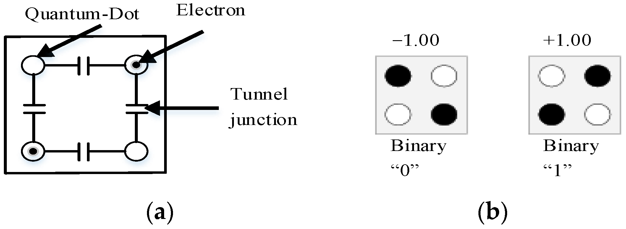
Figure 1. Schematics of QCA (a) cell, and (b) two structures logical values QCA cells.
Electronics 11 02320 g001
Figure 2. Clock zones for QCA wire.
Electronics 11 02320 g002
Figure 3. (a) Inverted MV gate, and (b) Regular MV gate.
Electronics 11 02320 g003
Figure 4. Schematic logic diagram of the novel FA circuits.
Electronics 11 02320 g004
Figure 5. The QCA layout with (a,b) FA circuits.
Electronics 11 02320 g005
Figure 6. Simulation results of the proposed (a,b) FA circuits.
Electronics 11 02320 g006
Figure 7. Logical diagram of the proposed 4-bit RCA circuit.
Electronics 11 02320 g007
Figure 8. The proposed (A,B) 4-bit RCA circuits.
Electronics 11 02320 g008
Figure 9. Simulation results for the proposed (A,B) 4-bit RCA circuits.
Electronics 11 02320 g009
Figure 10. Comparison and evaluation of QCA adders with (a) cost function, (b) complexity and (c) delay criterions.
Electronics 11 02320 g010aElectronics 11 02320 g010b
Figure 11. Thermal hotspots of the full adders (A) (FA-1) and (B) (FA-2) at 0.5 Ek.
Electronics 11 02320 g011
Table 1. Simulation parameters of the coherence vector tool.
ParameterValue
cell width18 nm
cell height18 nm
relative permittivity12.9
dot diameter5 nm
number of samples12,800
convergence tolerance0.001
clock high9.8 × 10−22 J
clock low3.8 × 10−23 J
clock amplitude factor2
radius of effect65 nm
layer separation11.5 nm
maximum iteration per sample100
Table 2. Comparison analysis of the novel FA circuits in comparison with others.
CircuitArea (µm2)Cell CountLatency (clock)NOT Gate CountCrossover Type
FA [1]0.0576011not required
FA-1 [8]0.043450.750not required
FA-2 [8]0.037430.750not required
FA [18]0.076610.54coplanar (rotated cells)
FA [19]0.0435912coplanar (clocking based)
FA [20]0.0475814coplanar (clocking based)
FA [21]0.0475612coplanar (clocking based)
FA [23]0.0253711not required
FA [24]0.043441.256not required
FA [25]0.0.39370.752not required
FA [26]0.03370.752not required
Proposed (a)0.031370.50not required
Proposed (b)0.027350.50not required
Table 3. Comparison analysis of the novel proposed 4-bit RCA circuits comparison with others.
CircuitArea (µm2)Cell CountDelay (clock)CostCost Function P, K, L = 1
FA [15]0.242371.50.3684
FA [19]0.292621.750.5149
FA [23]0.362502.750.9966
FA [27]0.2930820.5896
FA [28]0.372693.51.29154
Proposed (A)0.282331.250.3526.25
Proposed (B)0.252091.250.3126.25
Table 4. Energy consumption analysis of different multipliers at different tunneling energy levels at temperature 2 K.
FA CircuitAvg Leakage Energy (meV)Avg Switching Energy (meV)Avg Energy Dissipation (meV)
0.5 EK1 EK1.5 EK0.5 EK1 EK1.5 EK0.5 EK1 EK1.5 EK
FA-111.1232.9258.3749.142.8236.6260.2275.7494.99
FA-211.6433.1857.4538.1532.4927.3649.7965.6784.81
FA-[1]15.3744.8776.9261.8756.0351.6177.24100.9128.53
FA-[8]-113.9140.8772.1355.1348.141.3269.0488.97113.45
FA-[8]-214.1543.3777.9156.9846.5442.4771.1389.91120.38
FA-[18]29.1984.83148.5127.94108.8291.46157.13193.65239.97
FA-[19]19.2587.5102.8108.9995.1481.56128.19682.59184.32
FA-[20]16.9351.1191.37104.9192.4180.36121.84143.52171.73
FA-[21]14.9547.987.3292.1580.6369.3107.1128.53156.62
FA-[23]11.2232.9558.4364.0356.6649.4675.2589.61107.89
FA-[24]17.345.8976.9241.1134.3328.8658.4180.22105.78
FA-[25]15.4843.1175.9242.9136.7229.6558.3979.83105.57
FA-[26]13.9637.7763.8829.5524.6520.443.5162.4284.28
Publisher’s Note: MDPI stays neutral with regard to jurisdictional claims in published maps and institutional affiliations.