Article

Error Detection and Correction of Mismatch Errors in M-Channel TIADCs Based on Genetic Algorithm Optimization

1
School of Microelectronics, Tianjin University, Tianjin 300072, China
2
School of Information Science and Technology, Nantong University, Nantong 226019, China
*
Author to whom correspondence should be addressed.
Electronics 2022, 11(15), 2366; https://doi.org/10.3390/electronics11152366
Submission received: 2 July 2022 / Revised: 24 July 2022 / Accepted: 25 July 2022 / Published: 28 July 2022
(This article belongs to the Section Circuit and Signal Processing)

Abstract

:
In order to achieve higher system performance, a digital calibration technique for the sub-channel mismatches of time-interleaved ADCs (TIADCs) is proposed in this paper. The sine-fit-based estimation algorithm is introduced to estimate the channel mismatches and a calibration algorithm is proposed to compensate for the mismatches. Subsequently, the genetic algorithm (GA) is firstly utilized to detect the mismatch errors of the outputs of sub-channels after frequency domain filtering. The detected offset error and gain error are then corrected by performing the calibration algorithm, and the time errors are corrected by fractional delay filters based on Farrow structure. The spurious-free dynamic range (SFDR) is enhanced from 19.69 dB to 108.12 dB, and the signal to noise and distortion ratio (SNDR) is enhanced from 16.02 dB to 97.63 dB. The proposed technique is further validated on the FPGA. Compared with existing calibration techniques, the proposed technique has the advantages of simple algorithm structure, low hardware resource consumption, and high calibration accuracy and can be applied to the calibration of high-resolution (18-bit) TIADCs for low-frequency inputs.

1. Introduction

In view of a single ADC hardly meeting the requirements for both high sampling frequency and high resolution, designers have paid attention to the TIADC technique. This is a multi-channel data-parallel acquisition technique realized by the precise cooperation between each sub-channel [1,2,3]. Figure 1 shows the block diagram of an M-channel TIADC and its timing diagram. TIADCs are composed of M identical sub-ADCs working in parallel modes. Each sub-channel of a TIADC system consists of a sub-ADC with its own sampling and holding (S/H) circuit which is sampled and held at interleaved times. The sampling interval of each sub-channel is M T s . Therefore, the overall sampling rate of a TIADC system is M times higher than that of a single chip of ADC. In theory, this system increases the sampling rate of the ADC by a factor of M, and the sampling resolution of ADC is not reduced. A continuous analog input signal x(t) is sequentially sampled and digitized by the sub-ADCs to produce digital streams independently, and the TIADC system will eventually superpose each sub-channel output to produce a discrete digital output signal y[n] as is shown in Figure 1a.
However, due to the existence of different peripheral circuits and temperature variations of different sub-ADCs, the working conditions of each sub-channel cannot keep consistent, which results in channel mismatches. The channel mismatches mainly include the offset mismatch, the gain mismatch and the timing mismatch [4,5,6]. They introduce spurious spectra into the output spectrum, deteriorating the SNDR and SFDR of a TIADC, which severely degrades the performance of a TIADC system [7,8,9,10], especially for the high resolution requirement.
To solve the above limitation, multiple calibration techniques on TIADCs have been proposed. We classify them into two kinds: error detection and error correction. Error detection typically adds an additional auxiliary channel [11] to obtain the mismatch errors and then exploits fast interpolation for real-time calibration. This technique needs an additional channel, which increases the complexity and cost of the calibration system. In Ref. [12], the author used the difference between two adjacent channels as the judgment basis for the timing mismatch. The algorithm does not need complex computation such as multiplication but needs more sampling times to converge. In Refs. [13,14], the blind estimation algorithm was adopted to detect the timing mismatch of the system. The output of each channel can be directly utilized to estimate the sampling time error without a known signal in this algorithm. However, the error estimation performance of the blind estimation algorithm is worse than that of the non-blind estimation algorithm [15]. Error correction mainly includes offset, gain and timing mismatch correction, where the offset and gain mismatch error correction is a relatively simple technique. As a result, many works have been published recently on timing mismatch calibration. In Refs. [12,16], the phase of each clock was fine-tuned by the digital analog mixed method by adjusting the analog delay line. This method is easily affected by voltage, aging and other factors. In Refs. [17,18,19], the timing mismatch can be calibrated with a small number of conversions by the technique based on the split-ADC structure, which is limited to a low-resolution or moderate-resolution TIADC system. In Refs. [20,21], the author used a filter-bank structure to reconstruct the non-uniform sampled signals at the cost of an additional oversampling rate and higher hardware resource consumption. In Ref. [22], the author introduced an extra reference channel and used the correlation results to achieve the calibration, but the reference channel consumed hardware too. In Refs. [23,24], a technique based on the Hadamard transform was used to compensate for the timing mismatch which only required a fixed-coefficient FIR filter, thus simplifying the correction structure. However, only some special channel numbers have Hadamard transforms, which limits the application of this technique.
In this paper, we propose a genetic algorithm (GA)-based error detection and correction technique to optimize M-channel TIADCs. It is mainly divided into two steps: primary course correction and secondary fine correction. The sine-fit-based algorithm is utilized to estimate the existing offset, gain and timing mismatch, and these mismatch errors are roughly corrected with the derived correction algorithm. In the second step, frequency domain filtering is performed to eliminate the white Gaussian noise. Subsequently, the proposed GA technique is used to implement optimization and second detection [25]. Finally, the derived correction algorithm is used to implement the second fine correction for offset and gain mismatch, and a fractional delay filter based on Farrow structure is used to compensate for the remaining timing mismatch. As a result, the accuracy of the overall calibration is very high.
The highlights of this paper are as follows. Firstly, GA optimization is first proposed to detect and calibrate the offset, gain and timing mismatch at the same time. Secondly, no reference channel is added in the technique, which makes for small hardware consumption. Thirdly, the calibration technique can be applied to the calibration of high-resolution (18-bit) TIADCs for low-frequency inputs. The brief is organized as follows. In Section 2, an error detection and correction technique based on GA optimization is proposed. Section 3 simulates and analyzes the performance of the proposed technique. The hardware validation on FPGA is also presented. Finally, the conclusion and future directions are drawn in Section 4.

2. Materials and Methods

2.1. Model of TIADCs’ Mismatch Errors

The channel mismatch error model of a TIADC system is as shown in Figure 2. There are M sub-ADCs, and m is the channel index number. The aggregate sampling period is T s and the corresponding sampling rate is f s = 1/ T s . The adder o m is used to represent the offset mismatch error of each channel and the multiplier g m is used to represent the gain mismatch error of each channel. The delayer H m ( e jw ) is used to equal the clock delay and the timing mismatch error, and the timing mismatch error is r m T s . The sampling time can be expressed as follows.
t n = n M T s + m T s
Assuming the analog input signal is a single-frequency sine wave, its time domain expression is
x ( t ) = sin ( 2 π f i n t )
where f i n is the input signal frequency of the TIADC. Putting the existence of the three mismatch errors in the system into consideration, at the n-th sampling time, the output of the m-th channel can be expressed as follows:
x m [ n ] = ( 1 + g m ) sin ( 2 π f i n ( t n + r m T s ) ) + o m

2.2. Sine-Fit-Based Estimation and the First Correction

A sine wave includes four parameters, i.e., frequency, amplitude, phase and DC component [26,27]. The goal of sine fitting is to obtain the best fit values of the above parameters from the uniformly sampled sine wave signal. Here, we apply this method to the TIADC system, in which the error parameters of each channel are obtained by fitting the sampled sequence.
Formula (3) can be transformed as
x m [ n ] = A m cos ( 2 π f i n t n ) + B m sin ( 2 π f i n t n ) + C m
where
A m = ( 1 + g m ) sin ( 2 π f i n r m T s ) B m = ( 1 + g m ) cos ( 2 π f i n r m T s ) C m = o m
Assuming that the TIADC’s actual sampled value of the m-th channel at the n-th sampling time is y m [n], the goal is to find a set of A m , B m and C m to minimize the squared sum of the differences between y m [n] and x m [n], as shown in Formula (6).
ε = n = 1 N ( y m [ n ] x m [ n ] ) 2 = n = 1 N ( y m [ n ] A m cos ( 2 π f i n t n ) B m sin ( 2 π f i n t n ) C m )
Since the frequency of the input signal is known, only three parameters of the sine wave need to be considered. In order to find the best fit values for A m , B m and C m , the following matrices are established.
D = cos ( 2 π f i n t 1 ) sin ( 2 π f i n t 1 ) 1 cos ( 2 π f i n t 2 ) sin ( 2 π f i n t 2 ) 1 cos ( 2 π f i n t N ) sin ( 2 π f i n t N ) 1
y m = [ y m [ 1 ] y m [ 2 ] y m [ N ] ] T
S m = [ A m B m C m ] T
Then, Formula (6) can be expressed in matrix form as Formula (10).
ε = ( y m D · S m ) T ( y m D · S m )
Its least square (LS) solution is [28]:
S ^ m = ( D T · D ) 1 ( D T · y m ) = [ A ^ m B ^ m C ^ m ] T
Substituting Formula (11) into Formula (5), the estimated results of each sub-channel’s mismatch errors can be calculated as follows:
o m = C ^ m
g m = A ^ m 2 + B ^ m 2 1
r m T s = arctan ( A ^ m B ^ m ) 2 π f i n
According to the estimated mismatch errors, the correction algorithm can be derived. The parameters obtained in Formulas (12)–(14) are used as the initial parameters to reconstruct the signal to perform the first error correction on the output sampled data of the M-channel TIADCs. The output signals of each sub-channel before correction are given as x 1 , x 2 , …, x m , …, x M . We record the error parameters estimated by the sine-fit-based algorithm as o m , g m and r m .
Since both the offset mismatch and the gain mismatch are independent of the timing mismatch, the subtractors and the multipliers can be used for simple correction.
x ( n ) = x ( n ) o m
x ( n ) = x ( n ) 1 + g m
Since the sine-fit-based estimation method has very high error estimation accuracy for the offset error and the gain error (Ref. [29]), the timing mismatch error can be calibrated by performing the following process on x(n) :
x ( n ) = sin ( 2 π f i n ( t n + r m T s r m T s ) )
Expanding Formula (17) gives
x ( n ) = sin ( 2 π f i n ( t n + r m T s ) ) cos ( 2 π f i n r m T s ) cos ( 2 π f i n ( t n + r m T s ) ) sin ( 2 π f i n r m T s )
Transforming Formula (18) gives
x ( n ) = sin ( 2 π f i n ( t n + r m T s ) ) cos ( 2 π f i n r m T s ) 1 sin 2 ( 2 π f i n ( t n + r m T s ) ) sin ( 2 π f i n r m T s )
where sin ( 2 π f i n ( t n + r m T s ) ) can be equivalent to the signal x(n) , which has been obtained from Formula (16). Thus, the timing mismatch error is corrected.

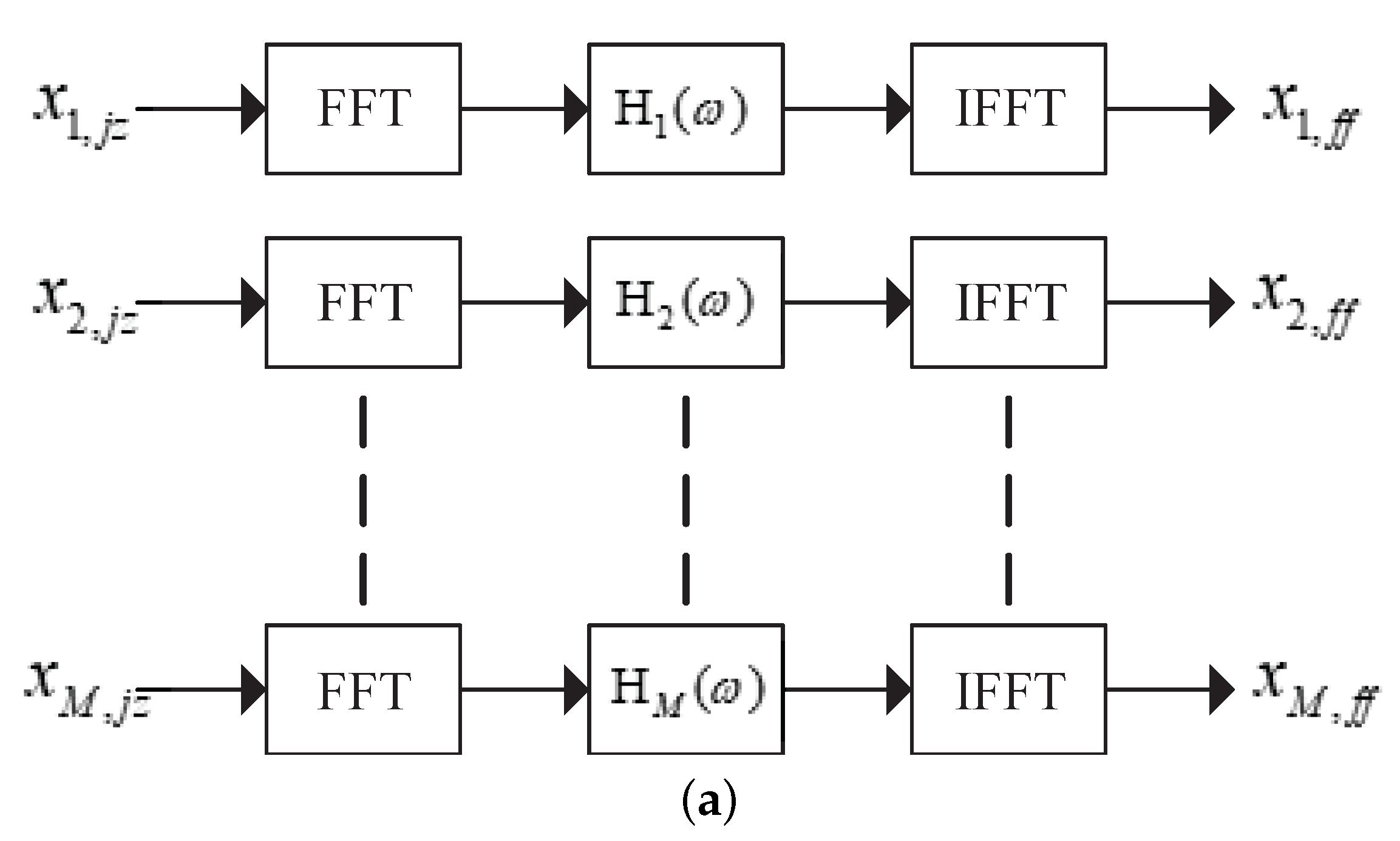
2.3. Frequency Domain Filtering Correction

Due to the inherent noise interference in sub-ADCs, frequency domain filtering correction is performed on the sampled data x(n) after the first correction. The block diagram of frequency domain filtering correction is shown in Figure 3a. The output signals of each channel after the first correction are given as x 1 , j z , x 2 , j z , …, x m , j z , …, x M , j z . Here, the procedure of frequency domain filtering correction is described as follows: (1) a set of band-pass filters H 1 (w), H 2 (w), …, H m (w), …, H M (w) are constructed to filter the noise according to the spectrum peaks of the signals x 1 , j z , x 2 , j z , …, x m , j z , …, x M , j z ; (2) the inverse fast Fourier transform (IFFT) is performed to obtain the filtered time domain signals, which are is recorded as x 1 , f f , x 2 , f f , …, x m , f f , …, x M , f f .
As is shown in Figure 3, frequency domain filtering correction is mainly used to filter the white noise in the signals after the first correction. It can help reduce the error caused by the white noise in the detection of the later error parameters. Then, the accuracy of the later error parameter estimation and correction can be improved.
The signals corrected by frequency domain filtering will be slightly deformed. However, the LS method cannot be used to estimate the deformed parameters.

2.4. Error Estimation and Correction Based on GA Optimization

Here, the GA optimization algorithm is used to perform the further estimation and correction for the signals x 1 , f f , x 2 , f f , …, x m , f f , …, x M , f f . The idea of the algorithm is summarized as follows: We take the minimum of errors between the signals to be further corrected and the standard signals as the optimization goal. Meanwhile, the error parameters are optimized in these iterations. Once the optimization is finished, the optimal error parameters can be obtained.
Throughout the optimization, these mismatch errors are determined by the GA and constantly iterated to obtain better parameters. The offset, gain and sampling time errors in each channel of the TIADCs can be detected when the optimization is done, as shown in Figure 3b.
The following steps are mainly involved in GA:
(i). Generation of chromosomes
Since the problem is to determine the offset, gain and sampling time errors, a random population with the number of individuals (P) is created, and three error phenotypes are contained in the individuals. Here, the way of binary coding is used. The advantage of binary coding is simple and can be implemented easily. The coding can be completed by 0 and 1, which makes the operations of the GA convenient. The relationship between the coding parameter u and the coding is as follows:
u = u m i n + a 2 l 1 ( u m a x u m i n )
where u is the parameter of binary coding and u m i n and u m a x are the minimum value and maximum value of u, respectively. a represents the encoded value and l represents the coding length.
(ii). Selection
A new binary population is formed by a part of the chromosomes selected from the old binary population randomly. The main selection methods of GA are proportion selection and ranking selection, and the error of the result is relatively large for proportion selection. Hence, the ranking selection is chosen in this paper. The essence of the selection is that the two parent chromosomes are selected according to the fitness of them, and the better the fitness, the bigger the chance to be selected.
(iii). Cross Over
The cross over operation is performed on the selected p chromosomes, and the gene exchange is carried out with a cross over probability. The function of the cross over is to recombine two chromosomes to generate two new ones. The cross over operation is performed among all chromosomes to generate new ones (children). The characteristics of the parent chromosomes are inherited in the new chromosomes, and the new chromosomes have advantages that the parent chromosomes do not have.
(iv). Mutation
The mutation operation is performed on new chromosomes generated by cross over with a mutation probability. Here, the mutation of a gene is realized by the mutation of a chromosome’s bit. One bit is randomly selected in the chromosomes and mutated, i.e., changing 0 to 1 or 1 to 0. The chromosomes obtained by mutation are added to previous chromosomes once again, i.e., parent and child chromosomes.
(v). Fitness function
The fitness function is used to evaluate the fitness of all these chromosomes after mutation. Here, the fitness function is chosen based on the error in sample values and the minimum error between the signal to be further corrected, and according to the principle of the sine fit calibration method, the input standard sine wave signal is taken as the optimization goal.
The fitness function F of an individual i is given as follows:
F = m e a n ( F m i )
F m i = m e a n ( e m i ( n ) )
e m i ( n ) = | x m ( n ) x m , f f ( n ) |
where x m (n) represents the m-th time interleaved ADC’s sampling signal without channel mismatch errors and x m , f f (n) represents the m-th channel’s signal obtained by filtering x m , j z (n) in the frequency domain. During the calculation, it is more reasonable to calculate the average values for individuals and channels.
(vi). Test
The fitness function F should satisfy the condition F F m i n , where F m i n is the minimum value of the fitness function F. If this condition is not satisfied, all the above steps are repeated until it is satisfied. When it is satisfied, the optimal value and its serial number I are output and the three mismatch errors written as o m , g m and r m T s will be detected by GA optimization, i.e., o m = o m (I), g m = g m (I), r m T s = r m (I) T s . The diagram for this algorithm is shown in Figure 4a.

2.5. The Second Fine Correction for Offset Error and Gain Error

The second fine correction for the offset error and the gain error is the same as the correction for the offset error and the gain error in Section 2.2. The subtractors and the multipliers can be used for the fine correction. As shown in Formulas (24) and (25),
x m , g a ( n ) = x m , f f ( n ) o m
x m , g a ( n ) = x m , g a ( n ) 1 + g m
The calibration for the timing mismatch error can be realized by Formula (19). However, its calibration is related to the frequency of the input signal f i n , which affects the calibration accuracy of the sampling time error. Therefore, a more appropriate algorithm is needed to calibrate the sampling time error accurately.

2.6. Calibration of Farrow Fractional Delay Filters

Now, the only timing mismatch error in the TIADC system is reconsidered and the timing mismatch error of m-th channel is still expressed as Δ t m = r m T s . Assuming that the Fourier transform of the input signal x(t) is x β (w), after sampling by TIADC system, the digital spectrum of the sequence can be expressed as
X ( w ) = 1 M T s m = 0 M 1 k = ( X β [ w k ( 2 π M T s ) ] · e j ( w k 2 π M T s ) r m · e j m k 2 π M )
If x(t) is a complex sinusoidal virtual signal e j w 0 t with an angular frequency of w 0 ( 2 π f 0 ), its Fourier transform is
X β ( w ) = 2 π σ ( w w 0 )
Substituting Formula (27) into Formula (26) gives
X ( w ) = 1 M T s m = 0 M 1 k = ( 2 π σ [ w w 0 k ( 2 π M T s ) ] · e j ( w k 2 π M T s ) r m · e j m k ( 2 π M ) )
It can be seen from Formula (28) that to recover the uniformly sampled spectra from the non-uniformly-sampled signal, an all-pass filter e j w r m is needed to correct the sampling time error.
According to Formula (28) and the time shift characteristic of the Fourier transform, the time domain delay Δ t m = r m T s of the signal is equivalent to multiplying the frequency domain value multiplied by e j w r m when the frequency domain changes. Therefore, an all-pass filter with the ideal frequency response e j w r m can be used to finish the correction as long as the Δ t m of each channel is detected. Since the coefficients of an all-pass filter are infinite, it cannot be implemented in FPGA. In order to implement real-time correction in FPGA, an FIR filter is used here to approximate it. Assuming that an N-order FIR filter is used to approximate h d (n), the transfer function is represented as follows:
H d ( z ) = n = 0 N 1 h d ( n ) z n
After GA optimization, we obtain ∣ r m ∣ < 1, showing that the filter is a fractional delay filter. With the aging of electronic devices and the influence of the environment, the mismatch error between channels is always changing. This increases the difficulty of calculating the coefficients of the fractional delay filters.
An efficient real-time correction algorithm can be implemented by Farrow structure filters. The coefficients of the fractional delay filters can be obtained in advance with this structure. Then, the coefficients of each filter are approximated by polynomials, and the N-order filter is further decomposed into N (P + 1)-order sub-filter banks. Once the filter coefficients are obtained, the timing mismatch error can be calibrated only by changing the delay value in the Farrow structure filter. We can expand h d (n) with respect to r m by performing the polynomial expansion to obtain
h d ( n ) k = 0 P b k ( n ) r m k , n = 0 , 1 , , N 1 , m = 0 , 1 , c d o t s , M 1
The b k n can be obtained by the Lagrange interpolation algorithm. The formula of the fractional delay filter is expressed in Formula (31). The output of the TIADC system filtered by fractional delay filters can be obtained. The expression of it is shown in Formula (32). Then, Formula (32) is recombined according to similar items of r to obtain the b k n .
H d ( z ) n = 0 N 1 k = 0 P b k ( n ) r m k z n = k = 0 P [ n = 0 N 1 b k ( n ) z n ] r m k = k = 0 P B k ( z ) r m k
h ( r ) = l = 0 , l k P r l k l , 0 k P
x c c r r ( n ) = k = 0 P h ( r ) x ( n k ) = k = 0 P l = 0 , l k P r l k l x ( n k )
Formula (33) is equivalent to the first P-term of Z r m expanded by a Taylor series. Therefore, the all-pass filter structure shown in Figure 4b can be obtained.

3. Results

To evaluate the effectiveness of the proposed method, the simulated results of a four-channel TIADC with a sampling frequency of 64 Ms/s are shown (the sampling rate of an 18-bit high-resolution ADC is usually slower than 20 Ms/s). The resolution of the TIADC is 18 bits. The added offset mismatch error is o m = [ o 1 , o 2 , o 3 , o 4 ] = [0.1, 0.2, 0.1, 0.3], the added gain mismatch error is g m = [ g 1 , g 2 , g 3 , g 4 ] = [0.0, 0.4, 0.3, 0.4], and the added timing mismatch error is r m T s = [10.0, 40.0, 50.0, 40.0]· T s . The input signal for the test is a single-frequency sine wave signal and its frequency is f i n = 1 kHz (for example, a speech signal).

3.1. Detection of Mismatch Errors

Table 1 shows the actual mismatch errors, the estimated mismatch errors by the sine-fit-based estimation algorithm and the detected mismatch errors by GA optimization (four significant digits are retained in the estimated results).
Table 1 is given to show that the sine-fit-based estimation algorithm has high estimation accuracy for the offset error and the gain error but low estimation accuracy for the sampling time error. The proposed algorithm based on GA optimization mitigates the effect of timing mismatch between sub-ADCs greatly.
Figure 5 expresses the optimization process of the GA. It can be found from Figure 5 that the value of fitness function F changes with the number of iterations. The proposed algorithm converges after about 60 iterations, and the minimum fitness function F of the best individual (I) is 2.355 × 10 3 .

3.2. Correction of Mismatch Errors

The output spectra of the four-channel TIADC before correction are shown in Figure 6a. It can be seen from Figure 6a that the spurious spectra appear in the frequencies of (16 MHz- f i n ), 16 MHz, (16 MHz+ f i n ), (32 MHz- f i n ) and 32 MHz, respectively. Due to the low frequency setting of f i n , spurious lines appear in (16 MHz- f i n ) and (16 MHz+ f i n ) coinciding with the spurious line in 16 MHz, and a spurious line appears in (32 MHz- f i n ) coinciding with that in 32 MHz. The description will not be repeated in subsequent simulations. The distortion is caused by the channel offset, gain and timing mismatch, which limits the dynamic performance of the TIADC severely. The SFDR of the TIADC is only 19.69 dB, the SNDR is only 16.02 dB and the effective number of bits (ENOB) is only 2.37 bits.
The output spectra of the four-channel TIADC after the first correction are exhibited in Figure 6b. The SFDR is improved to 57.10 dB, the SNDR is improved to 49.35 dB and the ENOB is improved to 7.91 bits. It can be found that the spurious spectra are reduced to some extent. However, the first estimation accuracy of the sampling time error is low and the calibration effect is limited. As a result, the performance of the TIADC system is still limited by the noise introduced by ADCs and the noise caused by the timing mismatch. For an 18-bit high-resolution TIADC, the performance is far from the requirements. In fact, the dynamic range (DR) of the TIADC needs to be greater than 100 dB.
The output spectra of the four-channel TIADC after the second fine correction for offset error and gain error are exhibited in Figure 6c. It can be seen that compared with the signal after the first calibration, the spurs caused by channel mismatch are reduced dramatically. In addition, the white noise introduced by ADCs is greatly decreased by the correction of frequency domain filtering. The SFDR is enhanced to 87.90 dB, the SNDR is enhanced to 80.38 dB and the ENOB is enhanced to 13.06 bits, which indicates the effectiveness of the proposed calibration method based on GA optimization.
The output spectra of the four-channel TIADC after the calibration of Farrow fractional delay filters are depicted in Figure 6d. Here, the order of the designed Farrow filter is 8, and the polynomial order for the Farrow structure is 5. The normalized bandwidth is 0.5. As can be seen, compared with Figure 6c, the spurs due to timing mismatch are further reduced. The proposed Farrow structure obtains an SFDR improvement of approximately 20 dB and an SNDR improvement of approximately 17 dB. The ENOB of the TIADC is enhanced from 13.06 bits to 15.93 bits. Moreover, this moment, the Walden figure of merit (FOM) is 100.44 fJ/conversion-steps with the system running at 64 MHz (Ref. [30]).
The situation of SFDR and SNDR versus normalized input frequency is illustrated in Figure 7a,b. It can be found that the SFDR and SNDR before calibration and after calibration decrease with the input frequency increment. The reason is the impact of the sampling time mismatch increases with the input frequency increment, which makes the proposed calibration technique have the best calibration effect for low-frequency inputs.

3.3. Comparison with Other Work

The characteristics of this calibration technique and several other TIADC calibration techniques are compared in Table 2. Compared with other calibration techniques, the proposed work can be used for offset, gain and sampling time mismatch without using the additional reference channel. The proposed work also has the advantages of being all digital and used in the calibration for high-resolution (16-bit, even 18-bit) TIADCs, although the calibration effect of high-frequency input is relatively poor.

3.4. Hardware Validation

Here, the hardware implementation of the calibration algorithm based on GA optimization is designed in Vivado. To implement the algorithm on the hardware, the key circuits of the algorithm are finished and converted into hardware description language (HDL). In this section, the implementation results of the synthesis and FPGA calibration are described.
The HDL design is synthesized to a gate-level netlist using the Vivado synthesis tool. As shown in Table 3, the Xilinx Virtex VII FPGA chip xc7vx485tffg1157-1 is used to validate the algorithm. The synthesized results exhibit that the design consumes only a few percentages of the hardware resources in the FPGA chip.
Figure 8a,b show the FPGA verification results of the proposed calibration technique. Here, the input frequency f i n is 5 MHz, and the clock frequency is 64 MHz. The offset, gain and timing mismatches are the same as those of the MATLAB simulation conditions. The results indicate that offset and gain mismatch spurs are removed completely and spurs due to timing mismatch are reduced dramatically. The SFDR is enhanced from 10.51 dB to 89.18 dB and the SNDR is enhanced from 6.11 dB to 82.66 dB. The effectiveness of the proposed TIADC calibration technique is validated by these experimental results.

4. Conclusions

An efficient all-digital calibration method based on genetic algorithm optimization which can detect and correct the offset, the gain and the timing mismatch in an M-channel TIADC system is proposed in this paper. By a sine-fit-based estimation algorithm, the mismatch errors are estimated, and the optimized mismatch errors are detected by the genetic algorithm. The calibration method is realized by the derived algorithm and a proposed fractional delay filter based on Farrow structure. The hardware implementation of the proposed algorithm is validated on the FPGA. The final results show that only a few FPGA hardware resources are used. The validation results show that this calibration technique is effective in reducing the time skew mismatch errors and improving the SFDRs/SNDRs of TIADCs. The proposed technique is also effective for the calibration of high-resolution TIADCs.

Author Contributions

Conceptualization, Y.L., X.L. and Y.Z.; methodology, Y.L. and X.L.; software, C.L. and G.N.; validation, C.L. and G.N.; formal analysis, Y.L.; resources, Y.L. and X.L.; data curation, C.L. and G.N.; writing—original draft preparation, C.L. and G.N.; writing—review and editing, Y.L., X.L., H.M. and Y.Z.; project administration, Y.L. All authors have read and agreed to the published version of the manuscript.

Funding

This research was supported in part by the National Natural Science Foundation of China (61927806, 62074085) and the technology project of Headquarters, State Grid Corporation of China (5700-202041397A-0-0-00).

Conflicts of Interest

The authors declare no conflict of interest.

References

  1. Black, W.C.; Hodges, D.A. Time interleaved converter arrays. IEEE J. Solid-State Circuits 1980, 15, 1022–1029. [Google Scholar] [CrossRef]
  2. Razavi, B. Design Considerations for Interleaved ADCs. IEEE J. Solid-State Circuits 2013, 48, 1806–1817. [Google Scholar] [CrossRef] [Green Version]
  3. Wei, W.; Ye, P.; Yang, K.; Zeng, H.; Song, J.; Zhao, Y. Compensation of dynamic nonlinear mismatches in time-interleaved analog-to-digital converter. IEICE Electron. Express 2019, 16, 1–6. [Google Scholar] [CrossRef] [Green Version]
  4. Kurosawa, N.; Kobayashi, H.; Maruyama, K.; Sugawara, H.; Kobayashi, K. Explicit analysis of channel mismatch effects in time-interleaved ADC systems. IEEE Trans. Circuits Syst. I Fundam. Theory Appl. 2001, 48, 261–271. [Google Scholar] [CrossRef] [Green Version]
  5. Parkey, C.R.; Mikhael, W.B. Time interleaved analog to digital converters: Tutorial 44. IEEE Instrum. Meas. Mag. 2013, 16, 42–51. [Google Scholar] [CrossRef]
  6. Salib, A.; Flanagan, M.F.; Cardiff, B. A High-Precision Time Skew Estimation and Correction Technique for Time-Interleaved ADCs. IEEE Trans. Circuits Syst. I Regul. Pap. 2019, 66, 3747–3760. [Google Scholar] [CrossRef] [Green Version]
  7. Monsurro, P.; Trifiletti, A. Calibration of Time-Interleaved ADCs via Hermitianity Preserving Taylor Approximations. IEEE Trans. Circuits Syst. II Express Briefs 2017, 64, 357–361. [Google Scholar] [CrossRef]
  8. Buchwald, A. High-speed time interleaved ADCs. IEEE Commun. Mag. 2016, 54, 71–77. [Google Scholar] [CrossRef]
  9. Razavi, B. Problem of timing mismatch in interleaved ADCs. In Proceedings of the 2012 IEEE Custom Integrated Circuits Conference (CICC), San Jose, CA, USA, 9–12 September 2012. [Google Scholar]
  10. Yin, M.; Ye, Z. First Order Statistic Based Fast Blind Calibration of Time Skews for Time-Interleaved ADCs. IEEE Trans. Circuits Syst. II Express Briefs 2020, 67, 162–166. [Google Scholar] [CrossRef]
  11. Huang, L.; Lin, B.Y.; Zhang, S.D. A Digital-Background TIADC Calibration Architecture and A Fast Calibration Algorithm for Timing-Error Mismatch. In Proceedings of the 2007 7th International Conference on ASIC, Guilin, China, 26–29 October 2007. [Google Scholar] [CrossRef]
  12. Li, J.; Wu, S.Y.; Liu, Y.; Ning, N.; Yu, Q. A Digital Timing Mismatch Calibration Technique in Time-Interleaved ADCs. IEEE Trans. Circuits Syst. II Express Briefs 2014, 61, 486–490. [Google Scholar] [CrossRef]
  13. Elbornsson, J.; Eklund, J.E. Blind estimation of timing errors in interleaved AD converters. In Proceedings of the 2001 IEEE International Conference on Acoustics, Speech, and Signal Processing, Salt Lake City, UT, USA, 7–11 May 2001. [Google Scholar]
  14. Elbornsson, J.; Gustafsson, F.; Eklund, J.-E. Blind equalization of time errors in a time-interleaved ADC system. IEEE Trans. Signal Process. 2005, 53, 1413–1424. [Google Scholar] [CrossRef] [Green Version]
  15. Zou, Y.X.; Xu, X.J. Blind Timing Skew Estimation Using Source Spectrum Sparsity in Time-Interleaved ADCs. IEEE Trans. Instrum. Meas. 2012, 61, 2401–2412. [Google Scholar] [CrossRef]
  16. El-Chammas, M.; Murmann, B. A 12-GS/s 81-mW 5-bit Time-Interleaved Flash ADC With Background Timing Skew Calibration. IEEE J. Solid-State Circuits 2011, 46, 838–847. [Google Scholar] [CrossRef]
  17. Guo, M.Q.; Sin, S.W.; Seng-Pan, U.; Martins, R.P. Split-based time-interleaved ADC with digital background timing-skew calibration. In Proceedings of the 2017 13th Conference on Ph.D. Research in Microelectronics and Electronics (PRIME), Taormina, Italy, 12–15 June 2017. [Google Scholar]
  18. Guo, M.Q.; Mao, J.J.; Sin, S.W.; Wei, H.G.; Martins, R.P. A 1.6-GS/s 12.2-mW Seven-/Eight-Way Split Time-Interleaved SAR ADC Achieving 54.2-dB SNDR With Digital Background Timing Mismatch Calibration. IEEE J. Solid-State Circuits 2020, 55, 693–705. [Google Scholar] [CrossRef]
  19. Hung, T.C.; Liao, F.W.; Kuo, T.H. A 12-Bit Time-Interleaved 400-MS/s Pipelined ADC With Split-ADC Digital Background Calibration in 4000 Conversions/Channel. IEEE Trans. Circuits Syst. II Express Briefs 2019, 66, 1810–1814. [Google Scholar] [CrossRef]
  20. Prendergast, R.S.; Levy, B.C.; Hurst, P.J. Reconstruction of band-limited periodic nonuniformly sampled signals through multirate filter banks. IEEE Trans. Circuits Syst. I Regul. Pap. 2004, 51, 1612–1622. [Google Scholar] [CrossRef]
  21. Li, D.; Zhu, Z.; Zhang, L.; Yang, Y. A background fast convergence algorithm for timing skew in time-Interleaved ADCs. Microelectron. J. 2016, 47, 45–52. [Google Scholar] [CrossRef]
  22. Ye, F.; Zhang, P.; Yu, B.; Chen, C.X.; Zhu, Y.; Ren, J.Y. A 14-bit 200-MS/s time-interleaved ADC calibrated with LMS-FIR and interpolation filter. In Proceedings of the 2011 IEEE International Conference of Electron Devices and Solid-State Circuits (EDSSC), Tianjin, China, 17–18 November 2011. [Google Scholar]
  23. Matsuno, J.; Yamaji, T.; Furuta, M.; Itakura, T. All-Digital Background Calibration Technique for Time-Interleaved ADC Using Pseudo Aliasing Signal. IEEE Trans. Circuits Syst. I Regul. Pap. 2013, 60, 1113–1121. [Google Scholar] [CrossRef]
  24. Qiu, Y.; Liu, Y.J.; Zhou, J.; Zhang, G.; Chen, D.; Du, N. All-Digital Blind Background Calibration Technique for Any Channel Time-Interleaved ADC. IEEE Trans. Circuits Syst. I Regul. Pap. 2018, 65, 2503–2514. [Google Scholar] [CrossRef]
  25. Liu, C.; Luo, X.; Niu, G.; Li, X.; Zhang, J. Error detection and correction of TIADC based on GA optimization. In Proceedings of the 2021 International Conference on Electronics, Circuits and Information Engineering (ECIE), Zhengzhou, China, 22–24 January 2021. [Google Scholar]
  26. Vucijak, N.M.; Radojevic, N.M. Three, Four and Seven Parameters Sine-fitting Algorithms Applied in the Electric Power Calibrations. In Proceedings of the International Conference on Computer as a Tool (EUROCON 2005), Belgrade, Serbia Monteneg, 21–24 November 2005. [Google Scholar]
  27. Belega, D.; Dallet, D.; Petri, D. Performance comparison of the three-parameter and the four-parameter sine-fit algorithms. In Proceedings of the 2011 IEEE International Instrumentation and Measurement Technology Conference (I2MTC), Hangzhou, China, 10–12 May 2011. [Google Scholar]
  28. IEEE Std 1241–2000; Std I. IEEE Standard for Terminology and Test Methods for Analog-to-Digital Converters. IEEE: New York, NY, USA, 2001; pp. 1–98. [CrossRef] [Green Version]
  29. Yang, K.J.; Shi, J.L.; Yang, H.Z. A TIADC mismatch calibration method for digital storage oscilloscope. In Proceedings of the 2017 13th IEEE International Conference on Electronic Measurement & Instruments (ICEMI), Yangzhou, China, 20–22 October 2017. [Google Scholar]
  30. Walden, R.H. Analog-to-digital converter survey and analysis. IEEE J. Sel. Areas Commun. 1999, 17, 539–550. [Google Scholar] [CrossRef] [Green Version]
  31. Duc, H.L.; Nguyen, D.M.; Jabbour, C.; Graba, T.; Desgreys, P.; Jamin, O.; Nguyen, V.T. All-Digital Calibration of Timing Skews for TIADCs Using the Polyphase Decomposition. IEEE Trans. Circuits Syst. II Express Briefs 2016, 63, 99–103. [Google Scholar] [CrossRef]
  32. Centurelli, F.; Monsurro, P.; Trifiletti, A. Efficient Digital Background Calibration of Time-Interleaved Pipeline Analog-to-Digital Converters. IEEE Trans. Circuits Syst. I Regul. Pap. 2012, 59, 1373–1383. [Google Scholar] [CrossRef]
  33. Kang, H.W.; Hong, H.K.; Park, S.; Kim, K.J.; Ahn, K.H.; Ryu, S.T. A Sign-Equality-Based Background Timing-Mismatch Calibration Algorithm for Time-Interleaved ADCs. IEEE Trans. Circuits Syst. II Express Briefs 2016, 63, 518–522. [Google Scholar] [CrossRef]
Figure 1. M-channel time-interleaved ADC. (a) Block diagram. (b) Timing sequence diagram.
Electronics 11 02366 g001
Figure 2. Model of M-channel TIADCs with offset, gain and timing mismatch errors.
Electronics 11 02366 g002
Figure 3. (a) Block diagram of frequency domain filtering correction and (b) channel mismatch error detection using GA.
Electronics 11 02366 g003aElectronics 11 02366 g003b
Figure 4. (a) Block diagram of error detection using GA. (b) Structure of Farrow filter based on polynomial approximation.
Electronics 11 02366 g004
Figure 5. Optimization process of the GA.
Electronics 11 02366 g005
Figure 6. Output spectra of the four-channel TIADCs before calibration (a), after the first correction (b), after the second fine correction for offset error and gain error (c) and after the calibration of Farrow fractional delay filters (d).
Electronics 11 02366 g006
Figure 7. SFDR (a) and SNDR (b) versus normalized input frequency.
Electronics 11 02366 g007
Figure 8. Output spectra of FPGA verification before calibration (a) and after calibration (b).
Electronics 11 02366 g008
Table 1. The detection of mismatch errors by sine-fit-based estimation algorithm and GA optimization.
Sub-ADCError Type
o m o m o m g m g m g m r m r m r m
ADC00.10.10000.0049 × 10 4 0.00.0000−0.0001 × 10 4 107.0251−0.0998
ADC10.20.20000.0098 × 10 4 0.40.40000.0195 × 10 4 4037.96930.4000
ADC20.10.10000.1610 × 10 4 0.30.3000−0.2488 × 10 4 5048.9833−0.2502
ADC30.30.3000−0.0146 × 10 4 0.40.4000−0.1366 × 10 4 4040.0438−0.0004
Table 2. Main characteristics parameters: a summary.
CharacteristicsRef. [21]Ref. [31]Ref. [32]Ref. [33]Ref. [22]This Work
All digitalnoyesyesyesyesyes
Mismatch typetimingtimingoffset,
gain and timing
timingoffset, gain,
timing and bandwidth
offset,
gain and timing
Add ref. channelnonoyesnonono
M (# of channels)444824
Wide freq. rangeyesyesnoyesyesyes
Resolution (bit)81112101418
Table 3. FPGA synthesis results.
FamilyVirtex VII
Devicexc7vx485tffg1157-1
LUT30480/303600 (10%)
LUTRAM13768/130800 (11%)
Flip-Flop30576/607200 (5%)
DSP516/2800 (18%)
Publisher’s Note: MDPI stays neutral with regard to jurisdictional claims in published maps and institutional affiliations.

