Abstract
With the increasing trend in the energy demand, power networks are transitioning from conventional generation systems to renewable energy sources (RESs). The energy is harvested from these RESs and fed to grid-connected inverters (GCIs), as the output power of major sources (e.g., solar and fuel cell) is mainly DC. However, owing to the lower output voltage of renewable RESs, power converters play a vital role in two-stage power systems for enhancing its lower value to a higher value. The basic requirement for the GCI is to maintain the constant output voltage for which it is essential to have a constant input voltage. Therefore, high gain and efficient power boost converters are required for a robust and reliable two-stage power system. This paper investigates the performance of an efficient model of a high step-up switched Z-source DC-DC converter (HS-SZSC) for grid-connected 3-phase H-bridge inverter applications. The proposed design achieves high voltage gain and eliminates the problems of circuit complexity by utilizing a smaller number of components, which makes it cost effective and highly efficient. The working principle is discussed in detail. To validate the proposed model, the performance of the conventional Z-source converter (ZSC) and proposed HS-SZSC employed with GCI is analyzed and compared for both normal and transient states through MATLAB simulations. The HS-SZSC with an open- and closed-loop system is tested at different loads (AC), representing varying power factor conditions, and results verify the suitability of the proposed design for grid-connected inverters. Lastly, another model is presented to resolve the issue of grid islanding in GCIs.
1. Introduction
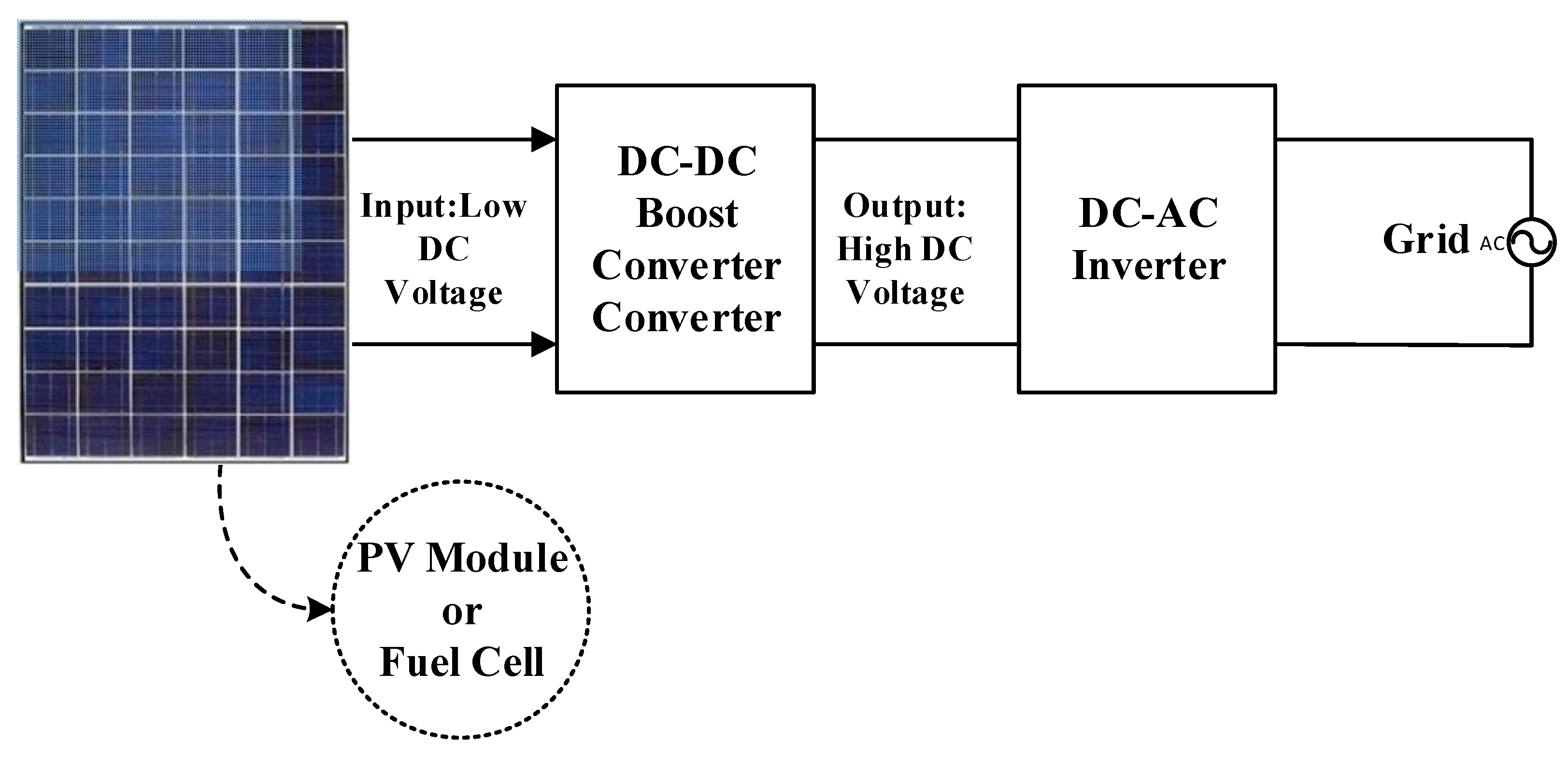
In the recent past, climate change has become a major concern, as conventional power generation sources, such as diesel, gas, coal, etc., have polluted the environment, leading to undesirable and drastic climate fluctuations [1]. Moreover, higher costs and increased carbon emissions have worsened the situation. Currently, the major challenge is to match the growing energy need while least affecting the atmosphere. To overcome this situation, renewable energy sources (RESs) are proven to be the best alternative, owing to their lower cost and non-polluting nature [2,3]. Generally, the energy is harvested from these sources and fed to grid-connected inverters (GCIs). Since the output voltage of RESs is low and varying in nature, power electronic converters are required to stabilize and enhance the voltage at the same time. In two-stage power systems, as shown in Figure 1, power converters play an important role to interface RESs with GCIs.

Figure 1.
The block diagram of the two-stage power conversion system.
Therefore, for better performance in a two-stage power conversion system, the converter must carry the advantages of reduced weight, less cost, semiconductor stress, etc. [4,5,6]. There are two types of converters, named non-isolated and isolated. The isolated converters [7,8,9] achieve the higher voltage gains by changing the turn ratio of the transformer; however, non-isolated converters control the duty cycle for achieving higher voltage gains, which affect the system performance and reduce the conversion efficiency. Numerous techniques have been reported in the literature to obtain a higher boost ratio and enhance the conversion efficiency. To illustrate, the converter in [10,11,12,13,14,15,16] utilizes a switched capacitor technique to attain higher gains at a reduced duty cycle. However, due to the switched capacitor, the pulsating current is produced at the input side, which results in poor load regulation. In [17], an extensive review of switch capacitor topologies as a part of voltage equalizer (VE) topologies is performed for the aim of performing maximum power tracking; however, switched capacitor converters are independent of duty cycle (D) and cannot perform the maximum power tracking for the individual model. The converter design in [18,19] involves an additional switch capacitor stage for improving the boost ratio, though it makes the circuit complex and bulky. To enhance the boost ability of DC-DC converters, a voltage lift technique combined with a coupled inductor is applied in [20]; nevertheless, the higher cost is a major concern for this topology. A coupled inductor-based topology employed with voltage multiplier cells is presented in [21,22,23,24] where higher input current is a drawback. The DC-DC boost converter topologies, such as the Cuk converter, Superlift Luo converter, and Sepic converter [5,6,25], are employed in two-stage power conversion systems for renewable energy applications. However, the lower value of the boost factor limits their performance.
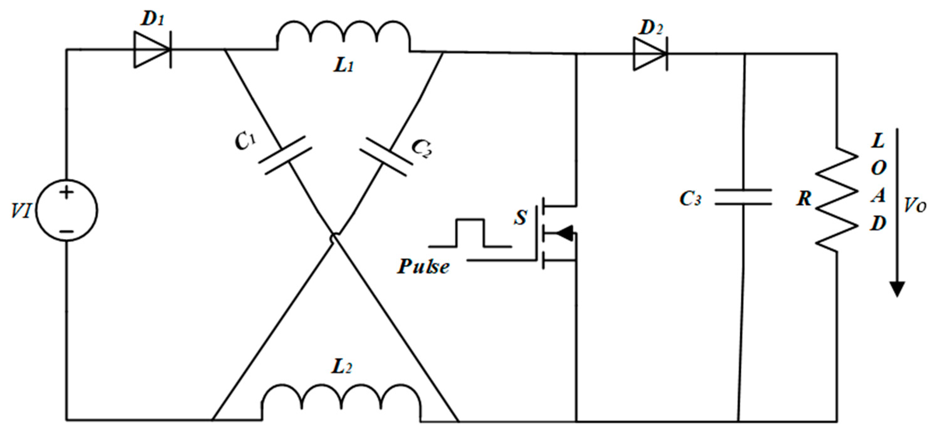
Apart from this, the Z-source network topology as shown in Figure 2 is the promising one among other topologies for renewable energy applications [26]. The Z-source network comprises two capacitors and two inductors connected in an X shape, which can solve the problems of limited boost factor and shoot through in conventional DC-DC converters to some extent. Numerous techniques have been employed with the Z-source network for improving the efficiency and voltage gain [27,28,29,30,31,32,33,34]. However, the major drawbacks associated with the Z-source converter are the higher starting current, limited voltage gain, higher voltage stress on components, discrete input, etc., which reduce its performance in real-world applications [35,36,37].
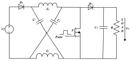
Figure 2.
The traditional Z-source DC-DC converter.
It is a well-known fact that the design of the DC-DC converter holds vital importance for the two-stage power conversion system. The better the performance of the converter, the higher the efficiency of the inverter. Several converters, such as cuk [5], superlift [6], Sepic [25], etc., are presented in the literature; however, several factors, such as lower boost factor, higher part count, etc., limit their performance. Thus, a new converter topology is required to overcome these issues.
The HS-SZSC topology is presented in [38]. The details of mathematical modeling, power loss and efficiency calculations, component designing, etc., for the HS-SZSC are discussed. Additionally, the theoretical analysis is verified through simulation and experimental results. From [38], it is worth noting that the proposed design exhibits several advantages, e.g., higher boost factor and reduced components that make it suitable for interfacing the RESs with the AC grid. Thus, in this paper, the performance of a Z-source converter topology termed as the high step-up switched Z-source converter (HS-SZSC) [38] is investigated for the grid-connected 3-phase H-bridge inverter application. In addition, the performance of HS-SZSC and conventional Z-source converter (ZSC) interfaced with 3-phase H-bridge inverter is analyzed and compared for normal and transient conditions to validate the effectiveness of the proposed model. Additionally, the HS-SZSC is tested for open- and closed-loops systems. Finally, one model is presented to resolve the islanding issue in grid-connected inverters (GCIs).
The remainder of this paper is organized in such a way that Section 2 explains the circuit configuration and working principle for the proposed circuit. The calculation of the gain factor is given in Section 3. Section 4 explains the operation of a 3-phase inverter interfaced with the switched converter. Section 5 compares the gain of the HS-SZSC with converters employed with GCIs. The simulation results are described in detail in Section 6. Finally, conclusions are drawn in Section 7.
2. Configuration and Operating Principle of the HS-SZSC
This section presents the physical structure and operating principle of the proposed switched converter.
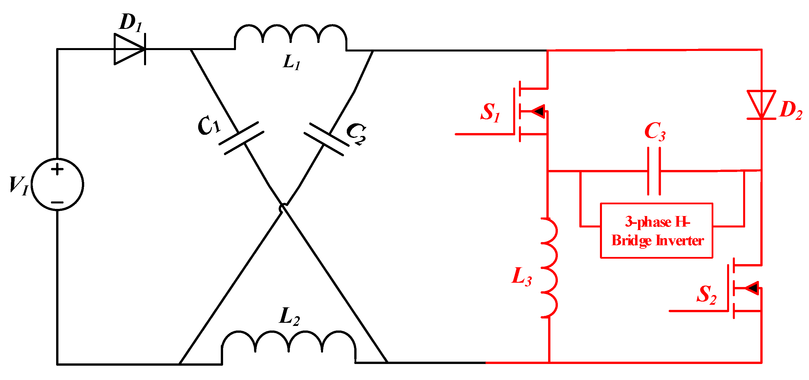
Figure 3 depicts the arrangement of the power circuit, which is composed of an impedance network (C1, C2, L1, L2), two MOSFETs (S1 and S2) that turn off and turn on at the same time and share the same gate signal, output capacitor C3, inductor L3, and load (3-phase H-bridge inverter). Apart from switch S2 and inductor L3, the structure of the new topology is similar to the conventional ZSC as shown in Figure 2. Thus, similar to the traditional ZSC, the proposed design has two operating states, i.e., switch-on period and switch-off period.
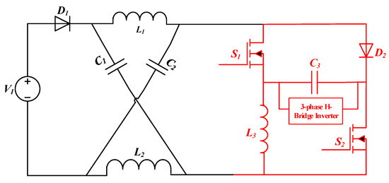
Figure 3.
The proposed high step-up switched Z-source converter (HS-SZSC).
During the switch-on period, capacitors will supply energy to inductors; hence, the inductor current will increase and store the energy, while the capacitor voltage will be rising during the switch-off period, as inductors will release the energy to capacitors and the load [38]. The following section demonstrates the calculation of the boost factor for the proposed HS-SZSC.
3. Calculation of Gain Factor
This section demonstrates the calculation of the gain factor. The gain factor is described as the ratio of the output voltage to the input voltage. Applying the Kirchhoff’s voltage and current laws (i.e., KVL and KCL) on the proposed converter in both states, the following equations can be obtained:
- State-1
- State-2
4. HS-SZSC Interfaced with 3-Phase Inverter (GCI)
The GCIs are classified according to the power range, which can vary from a few watts to thousands of watts. The power range up to 5 kW is suitable for household applications; however, a power range higher than 5 kW is utilized in larger buildings. Moreover, the power generation less than 5 kW is called microinverters [2]. Generally, The GCI contains two basic features.
- Phase matching.
- Reaction to the power outage: addressing an islanding issue.
The output voltage of the GCI must be in phase with the mains supply. The GCI senses the phase of the main supply and produces a phase-matched AC supply.
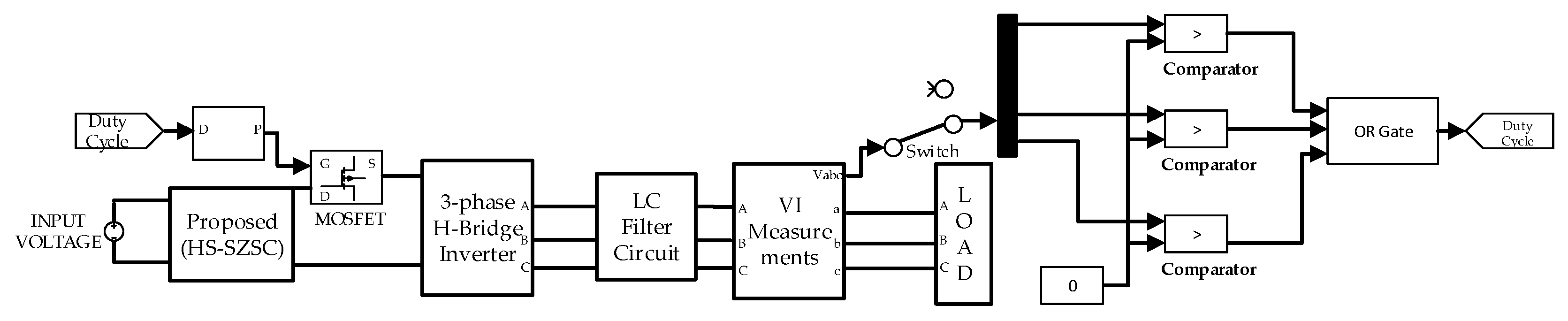
Moreover, islanding is a critical condition occurring in a power system in which a distributed generator, e.g., the solar system supplies the power to the grid even when the power from utility does not exist [37,38,39,40]. One of the key advantages of grid-connected inverters is that it disconnects automatically in the events of the main power failure or no-load conditions. This safety feature protects the line workers and avoids inverter loss. Thus, a simulation model based on HS-SZSC and GCI is proposed in this research article that will be discussed later in Section 6.
This section presents the circuit configuration, PWM technique, and inverter side closed-loop control for a switched converter interfaced with the inverter.
4.1. Circuit Configuration
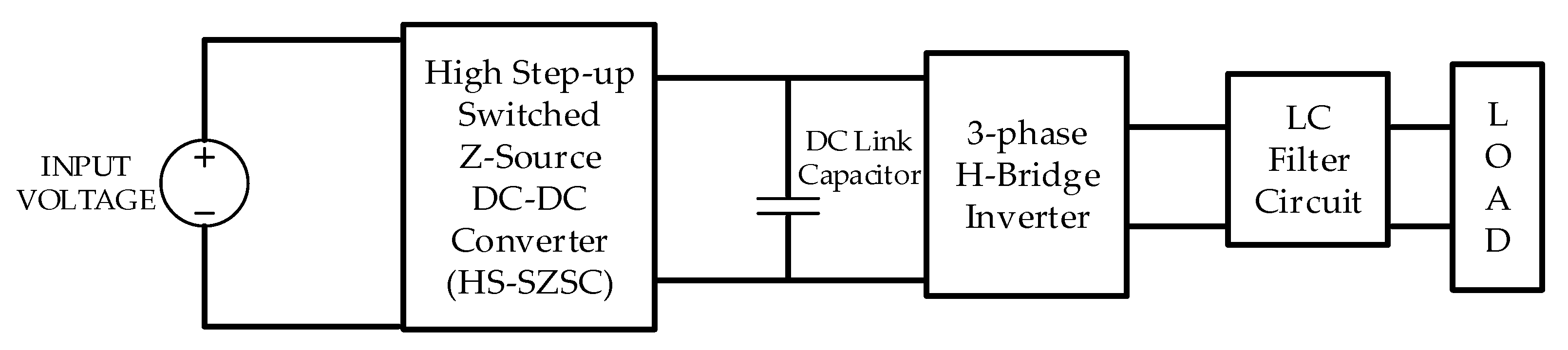
Figure 4 shows the circuit arrangement for the two-stage power conversion system with the switched converter. The circuit consists of a DC power supply connected with the HS-SZSC [38] to boost the voltage significantly to the higher levels. The output of the converter is interfaced with the famous 3-phase H-bridge inverter in order to generate an AC output power. The output of the inverter will pass through an LC filter to reduce the harmonics.

Figure 4.
Proposed HS-SZC interfaced with 3-phase inverter.
4.2. Sinusoidal Pulse Width Modulation (SPWM)
The pulse width modulation (PWM) is widely used in different applications, e.g., variable speed drives, motor control, etc. The most common technique used for inverters is sinusoidal PWM (SPWM). In this method, a reference sinusoidal waveform with the frequency fr is compared with a triangular carrier waveform having the frequency fC in order to create the switching signals [41,42]. The output frequency of the inverter is defined by the reference signal frequency, which also controls the modulation index Ma. The modulation index Ma is defined as
where Vr and VC define the voltages across reference and carrier signals, respectively. Moreover, the number of pulses per half cycle is defined by carrier frequency fr. Figure 5 shows the method of generating signals for the 3-phase H -bridge inverter.
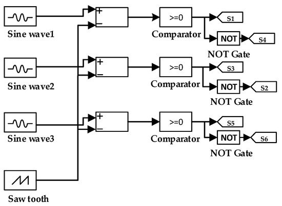
Figure 5.
The gating signal generation for 3-phase inverter.
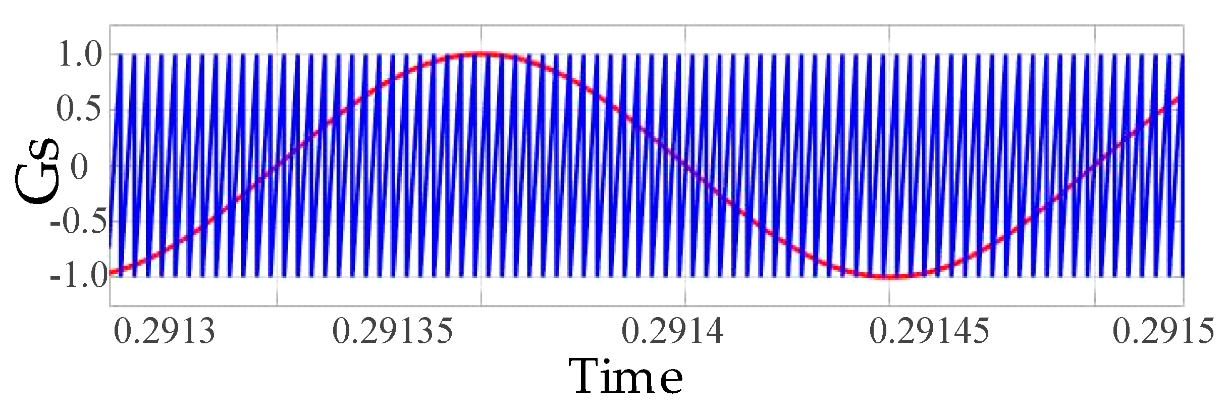
In this method, three reference sinusoidal waveforms are separately compared with a common sawtooth carrier waveform as in Figure 6. Each comparison results in the switching pulse of the corresponding switch. Since one leg contains two complementary switches, control signals for both the switches in one leg will be opposite in nature, which are produced by using the NOT gate in the circuit.

Figure 6.
Comparing the sinusoidal waveform with the sawtooth carrier waveform.
4.3. Inverter-Side Controller
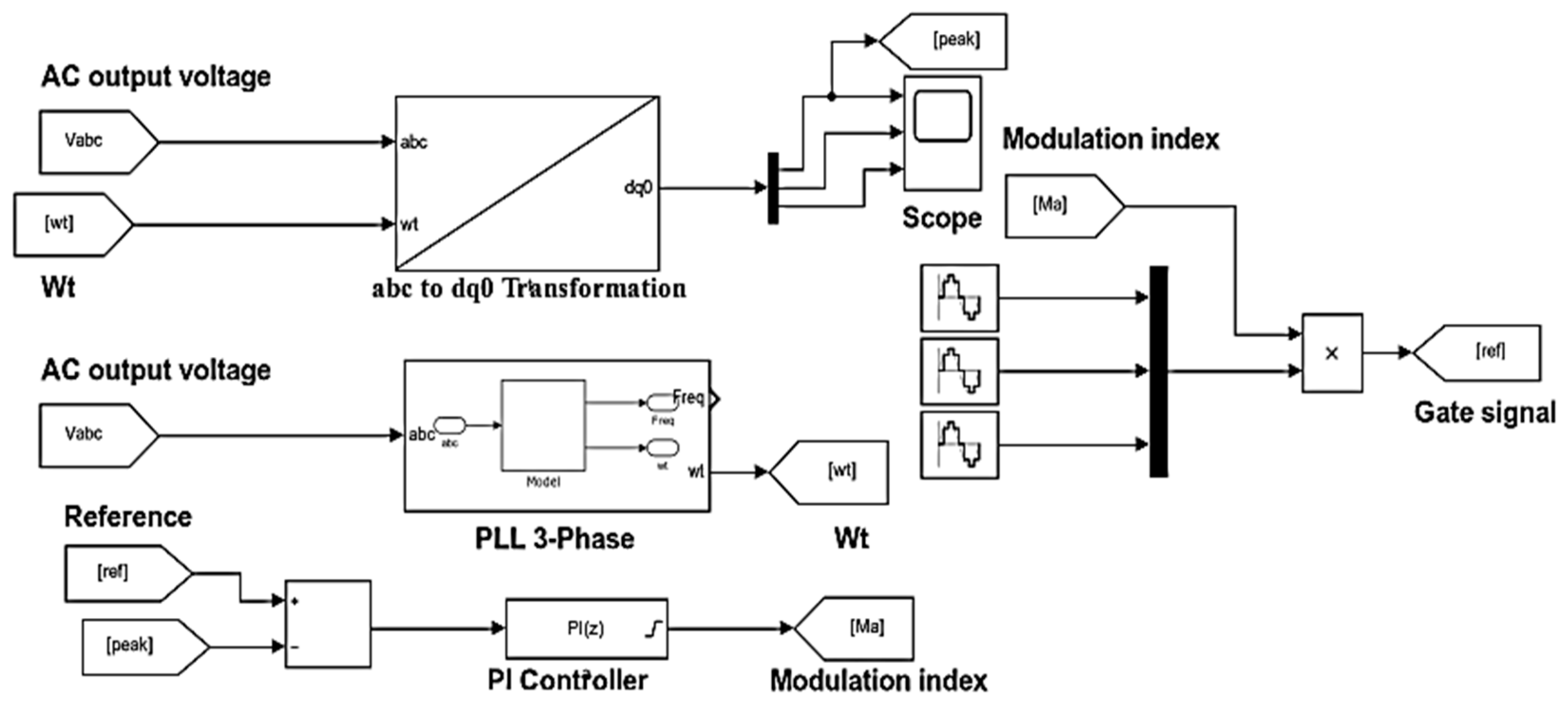
To test the system for a closed-loop and verify the performance of the HS-SZSC, the proportional integral (PI) controller is employed with the inverter. Figure 7 displays the inverter-side controller. It can be seen that abc to dq0 transformation, also known as park transformation, is used. Park transformation refers to the conversion of the three-phase signal (abc) to rotating reference frame (dq0). In contrast to the abc system, the dq0 frame offers easier control, thus the system can be controlled by using only one controller. Moreover, the PI controller with DC quantities offers a reliable and effective control solution; therefore, the output of the inverter is transformed using abc to dq0 transformation in MATLAB. Furthermore, the angular position of the rotating frame (Wt) is obtained using the phase lock loop (PLL) model. Later, the three-phase voltage (Vabc) along with the angular position of the rotating frame (Wt) is fed to the transformation block. The obtained dq0 components are compared with the reference signal, which generates the error signal. The error signal is fed to the PI controller, which outputs the desired signal. The PI controller parameters are taken as KP = 0.001 and KI = 0.5.
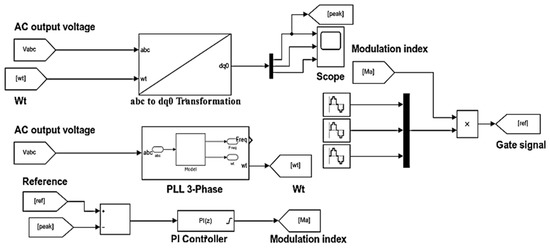
Figure 7.
Diagram for the inverter-side controller.
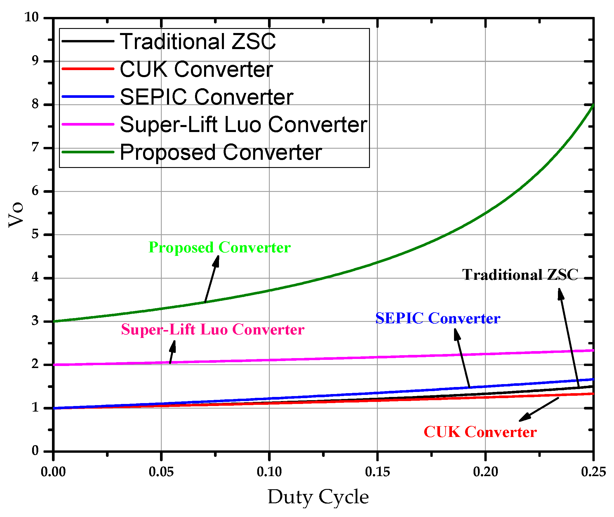
5. Comparison of Voltage Gains
To estimate the converter’s performance, the boost ability is the significant one among other properties of the DC-DC converter. In this section, traditional converters employed with GCIs are compared with the proposed HS-SZSC [38]. The converter topologies presented in [5,6,25,26] are compared with the proposed switched converter. The graph shown in Figure 8 describes the relationship between the duty cycle and gain factor. From Figure 8, it can be realized that the proposed converter obtains the higher voltage gain in comparison to other conventional converters. With this feature, the switched converter can be employed with GCIs at a lower cost and higher efficiency.
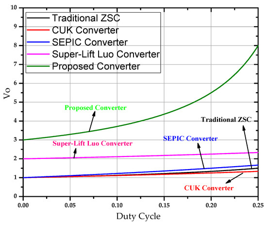
Figure 8.
Comparison in the boost ability for the proposed and conventional converters.
6. Results and Discussions
The block diagram for a two-stage power conversion system utilizing the switched converter is shown in Figure 4. The system consists of a DC power supply followed by a HS-SZSC whose output relates to a 3-phase H-bridge inverter. The important parameters adopted for simulations are specified in Table 1 [38].

Table 1.
Simulation parameters.
In this research, the simulations are carried out for three cases i.e., normal condition, transient condition, and addressing an islanding issue in GCIs. For normal conditions, the HS-SZSC is supplied with a fixed input voltage VI = 35 V; however, for the transient state, the HS-SZSC is fed with the variable supply voltage to exhibit the transient characteristics.
In addition, the simulation results are compared with traditional ZSC with similar conditions to validate the performance of the proposed model. The simulation results for conventional ZSC and HS-SZSC for all cases are given through the following case studies.
6.1. Case 1: Normal Conditions
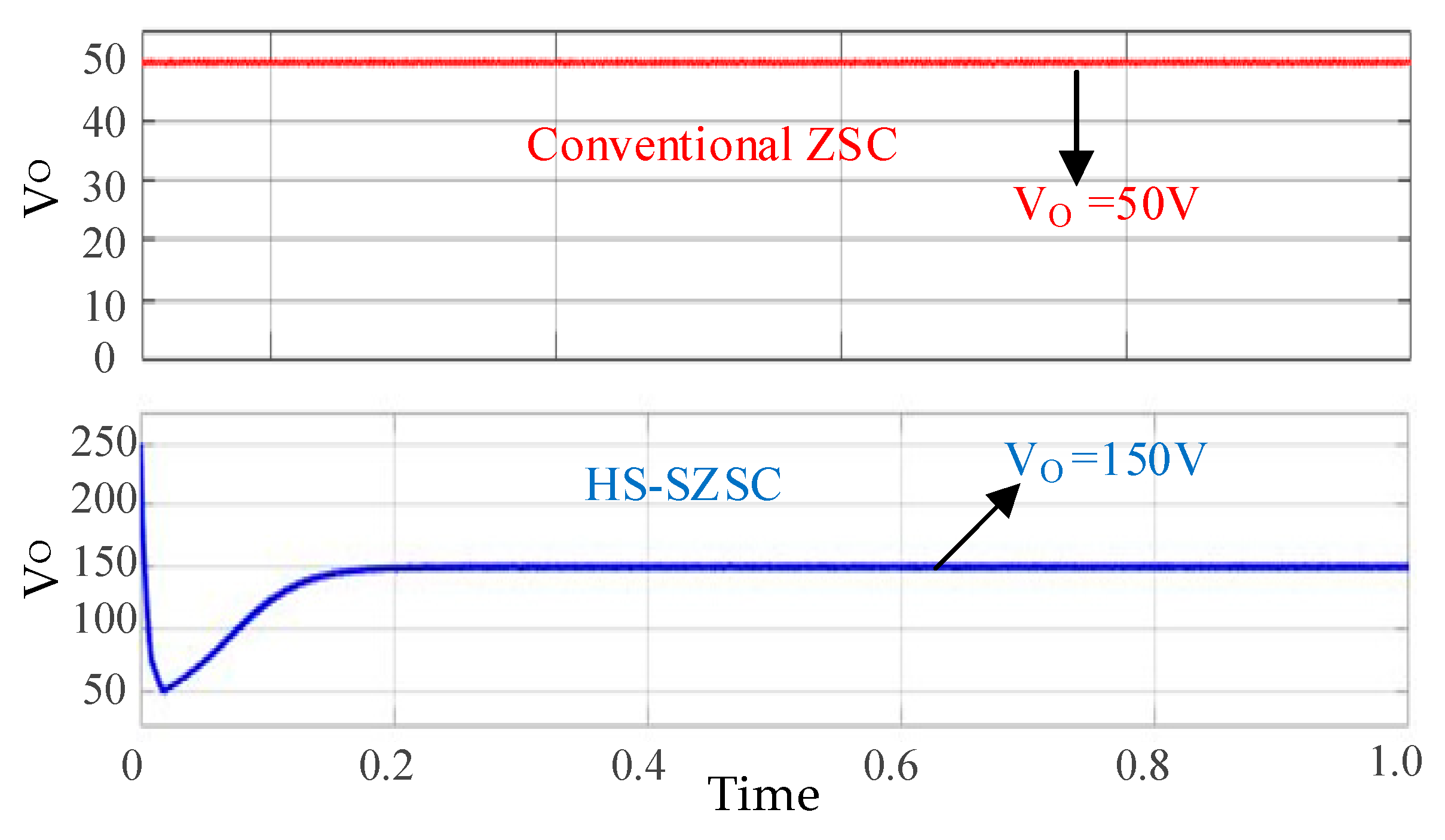
In this case, the HS-SZSC and ZSC are fed with a fixed supply voltage of VI = 35 V. The simulation results for both the converters are manifested in Figure 9, Figure 10, Figure 11 and Figure 12. Figure 9 presents the output voltage of conventional ZSC and HS-SZSC. From Figure 9, for the same input voltage (VI = 35 V) and duty cycle (D = 0.15), the HS-SZSC achieves significantly higher output voltage (VO = 150 V) compared to conventional ZSC (VO = 50 V). Since the gain factor is described as the ratio of the output voltage to the input voltage thus, the gain factor at D = 0.15 for the HS-SZSC and ZSC are G = 4.28 and G = 1.42, respectively. Hence, the HS-SZSC clearly achieves a higher gain factor in comparison with traditional ZSC.
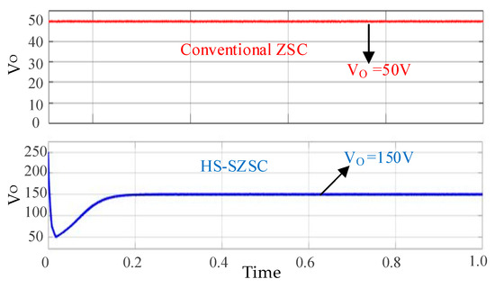
Figure 9.
The output voltage waveforms for the ZSC and HS-SZSC.
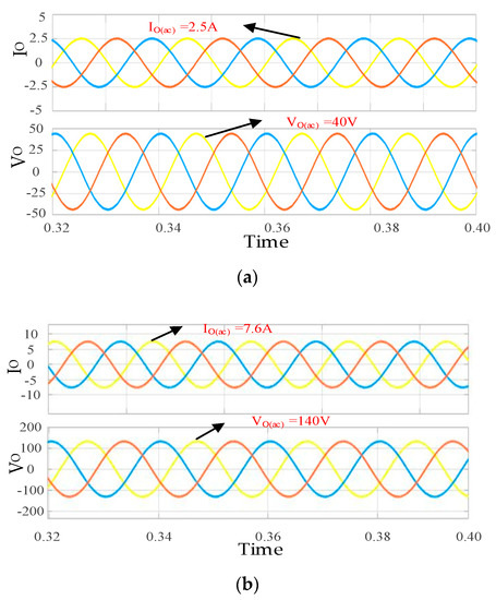
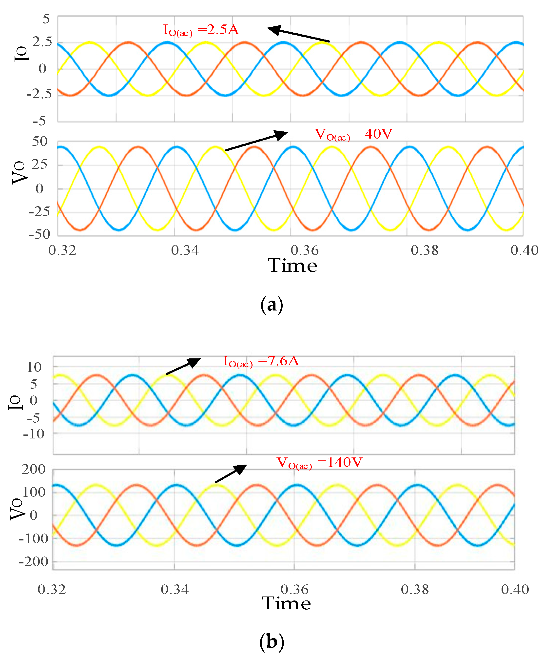
Figure 10.
The output voltage and current waveforms of the 3-phase H-bridge inverter with ZSC and HS-SZSC; (a) conventional ZSC and (b) proposed HS-SZSC.
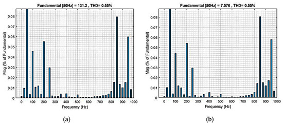
Figure 11.
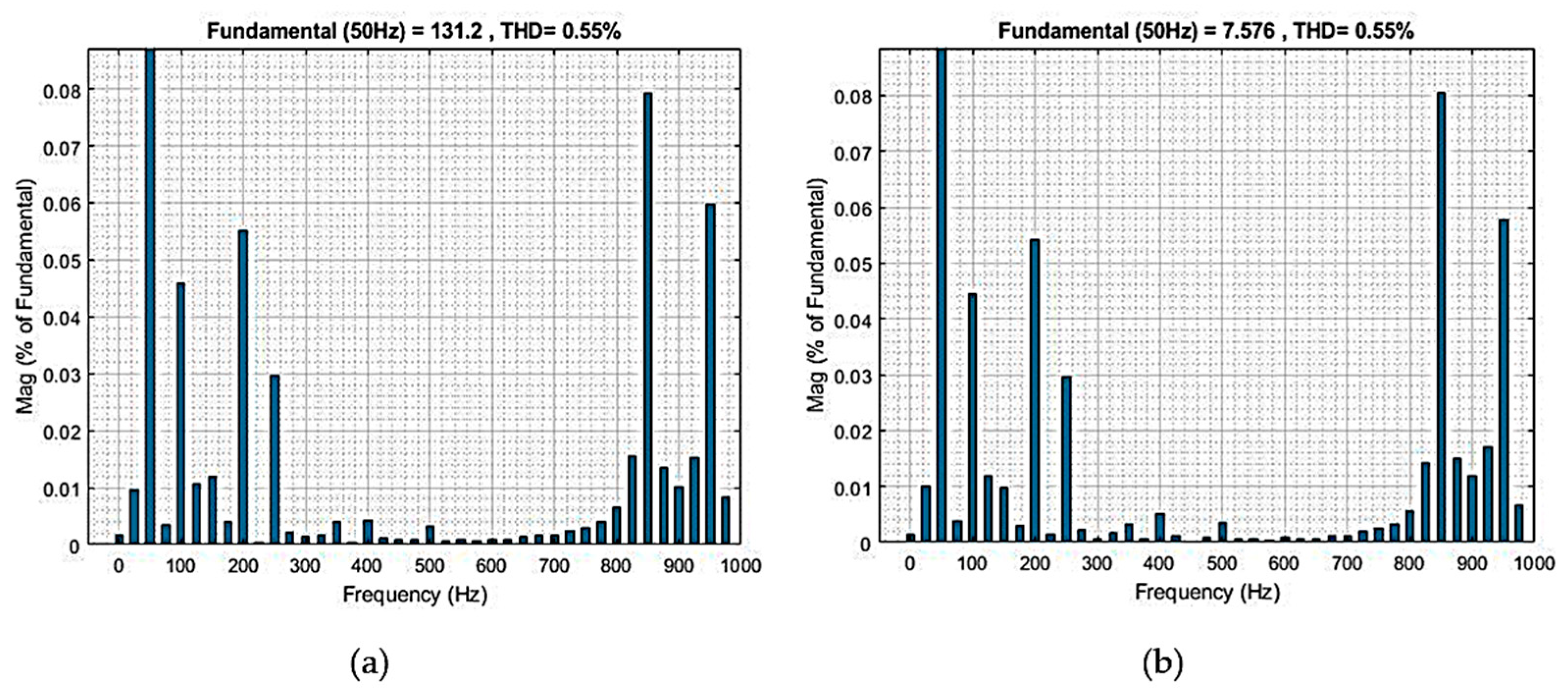
The THD values of output voltage and current for the 3-phase inverter interfaced with HS-SZSC, (a) voltage waveform, and (b) current waveform.
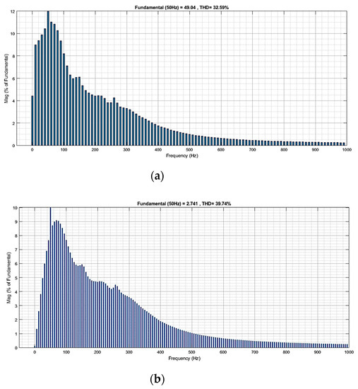
Figure 12.
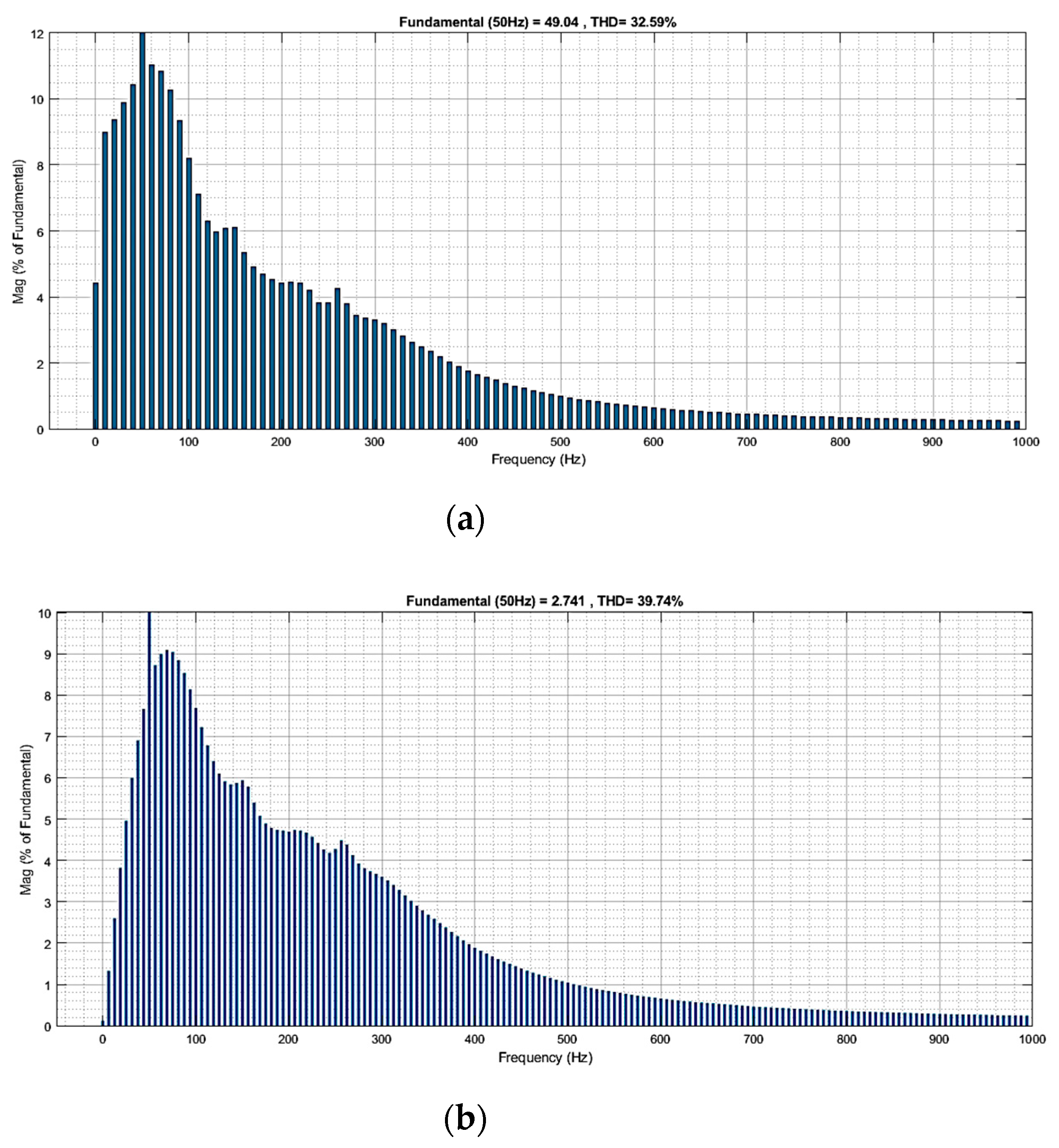
The THD values of output voltage and current for the inverter with ZSC, (a) voltage waveform, and (b) current waveform.
Since the output of both converters are interfaced with a 3-phase H-bridge inverter, Figure 10 shows the output voltage and current waveforms for these converters. From Figure 10a, the peak voltage and current values for the ZSC are VO(ac) = 40 V and IO(ac) = 2.5 A, respectively. On the other hand, for proposed HS-SZSC, these values are found to be VO(ac) = 140 V and IO(ac) = 7.6 A. This can be justified by considering the DC gains of both the converters at the aforementioned conditions, i.e., HS-SZSC (4.28) and ZSC (1.42). Since the output of the converter is fed to the inverter as input, thus, the lower DC gain will produce a reduced ac voltage and current. It is evidenced that, compared to conventional ZSC, the proposed converter achieves significantly higher voltage and current values on the inverter side as well.
The total harmonic distortion (THD) is one among the considerable factors for the inverter operation.
Thus, for the efficient operation, this value should be as low as possible. The THD curves for the inverter interfaced with the ZSC and HS-SZSC are given in Figure 11 and Figure 12, respectively. From Figure 11 and Figure 12, it can be found that the THD value for both output voltage and current is 0.55% when the proposed HS-SZSC is interfaced with the inverter, which complies well with the IEEE standard [43,44]. However, for the inverter with the conventional ZSC, the values of the THD are 32.59% for voltage and 39.74% for current. The higher values of THD for ZSC-inverter combination are because of higher ripples at the output of the ZSC, thus the inverter supplied with such a voltage tends to have higher THD. Further it can be noticed that the proposed design achieves a smaller value of THD, thus the efficiency of the inverter interfaced with HS-SZSC will be higher, compared to the ZSC.
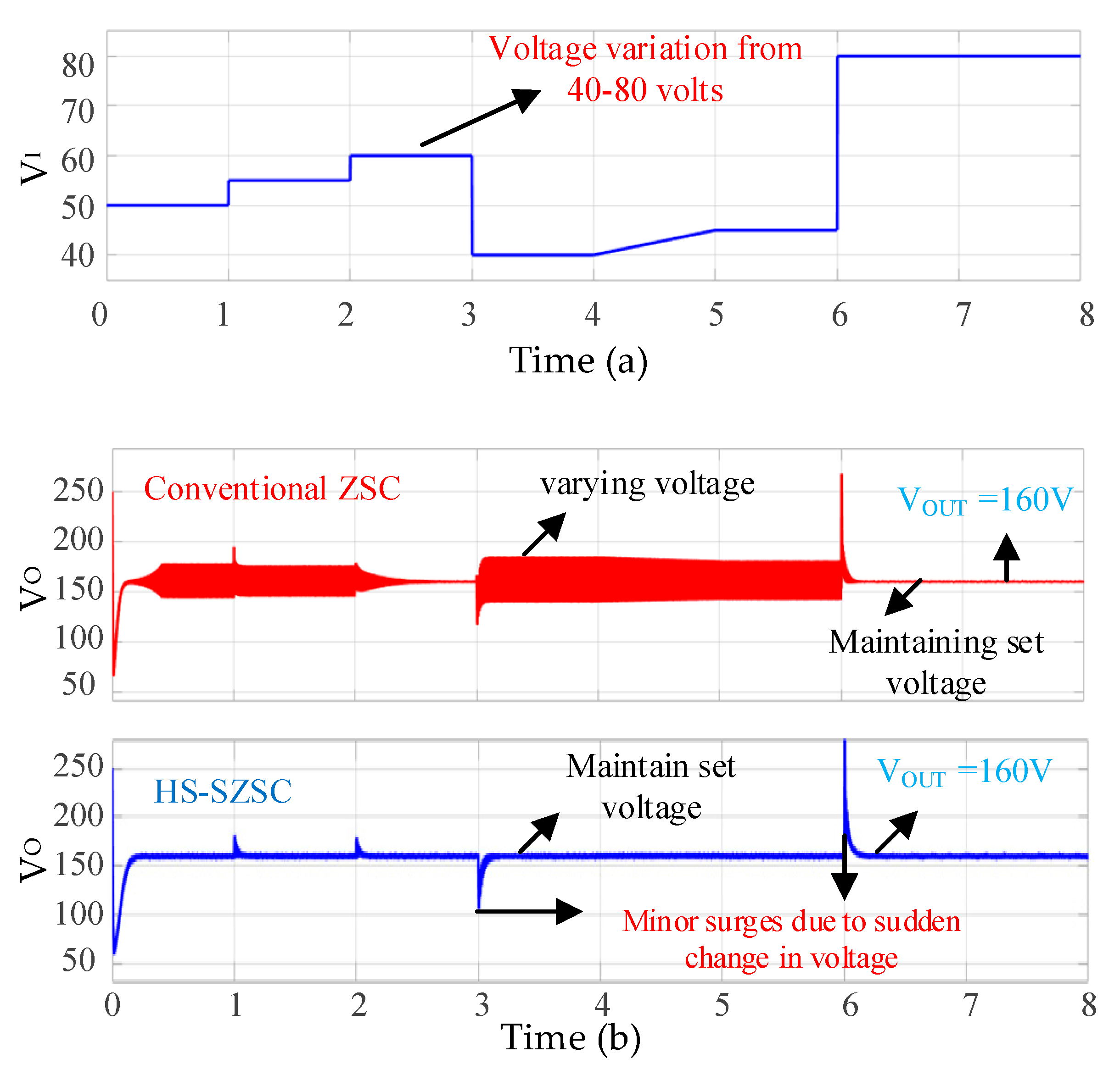
6.2. Case 2: Transient Conditions
In this case, the transient state was introduced by supplying the HS-SZSC and ZSC with a variable supply voltage. The voltage is varied between 40 and 80 V. The simulation results for both the converters in this case study are demonstrated in Figure 13 and Figure 14. Figure 13 presents the variable input voltage along output voltages of conventional ZSC and HS-SZSC during this state. The set value of the output voltage for both converters is 160 V. From the simulation result in Figure 13, the output of the ZSC is continuously varying with the input voltage. It is only constant when the input voltage reaches higher than 60 V. This point can be observed from the waveform during the time from 2 to 3 s and 6 to 8 s. The reason behind this is the continuous change in input voltage and switch stress. When the voltage is between 40 and 60 volts, the ZSC has to generate the gain of 4.0–2.66 to maintain the output voltage at 160 volts, thus with the higher gain, the stress on the switches increases that produces the ripples at the output voltage.
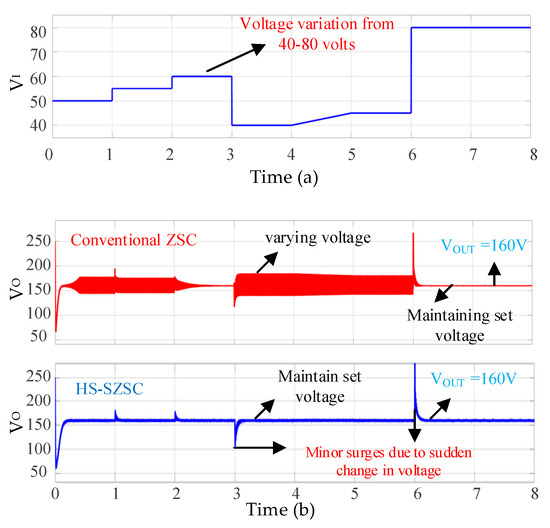
Figure 13.
(a) The variable input voltage for the conventional ZSC and HS-SZSC (variation between 40–80 V), (b) the DC output voltage for the conventional ZSC and HS-SZSC.
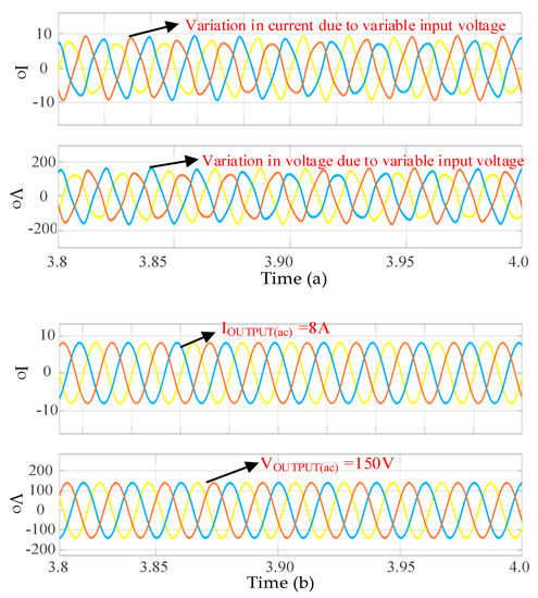
Figure 14.
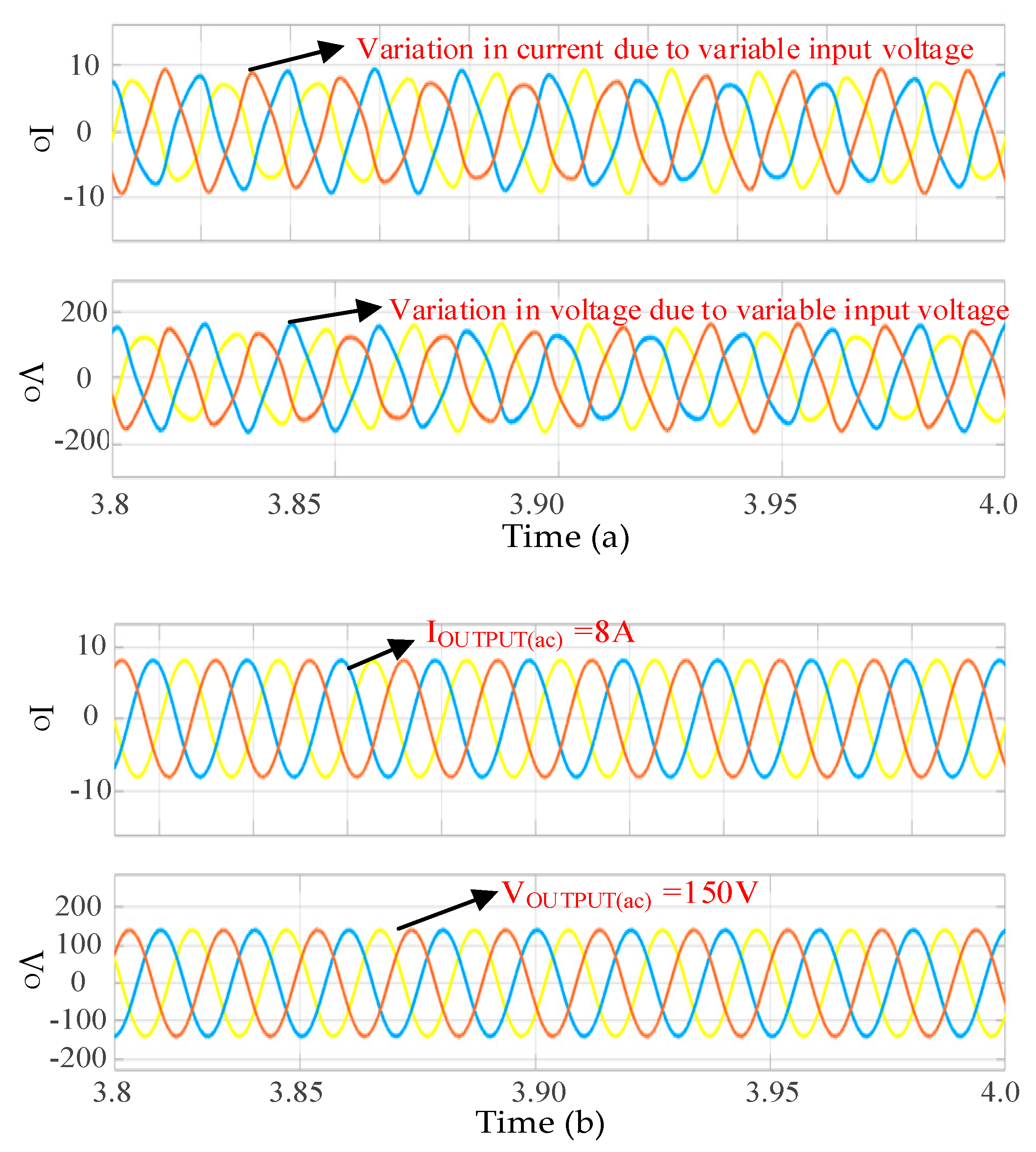
(a) The output voltage and current of the 3-phase inverter interfaced with the ZSC during the transient state, (b) the output voltage and current of 3-phase inverter interfaced with HS-SZSC during transient state.
On the other hand, the proposed HS-SZSC maintains the constant voltage throughout the input supply. There are minor surges for a very short time (milliseconds), which is because of a sudden rise in the input voltage. The proposed inverter design performs well while comparing to the conventional converter. The reason behind this is higher gain, reduced output voltage ripples (DC output), and reduced current and voltage stress on the switches.
Apart from this, the output voltage and current waveforms of inverter interfaced with both converters are given in Figure 14. From Figure 14, the output voltage and current of inverter interfaced with the ZSC vary continuously due to the variation in the input voltage. This can harm the load connected to it. However, on the other side, the same inverter interfaced with the HS-SZSC maintains the constant output voltage throughout the voltage range. Hence, the proposed HS-SZSC performs better during the transient conditions as compared to the conventional ZSC, which further justifies the suitability of the proposed design for GCI applications.
6.3. Case 3: Islanding Issues in GCIs
Aside from the above analysis, this paper also focuses on the islanding issue of the grid. Addressing an islanding issue is much important for GCIs in order to protect the line workers and avoid the inverter loss. In this paper, to address the islanding issue, one Simulink model using the switched converter is built using MATLAB, which is shown in Figure 15.

Figure 15.
The block diagram representation of the model to address the islanding issue of GCIs.
In this model, a MOSFET is utilized with the switched converter at the output side. During the no-load condition, the manual switch is activated by the logically compared output, which operates MOSFETs accordingly. Hence, no current flows through the line during the no-load condition as shown in Figure 16.
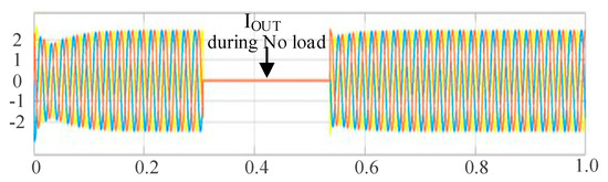
Figure 16.
The output of the inverter during a sudden loss of the load.
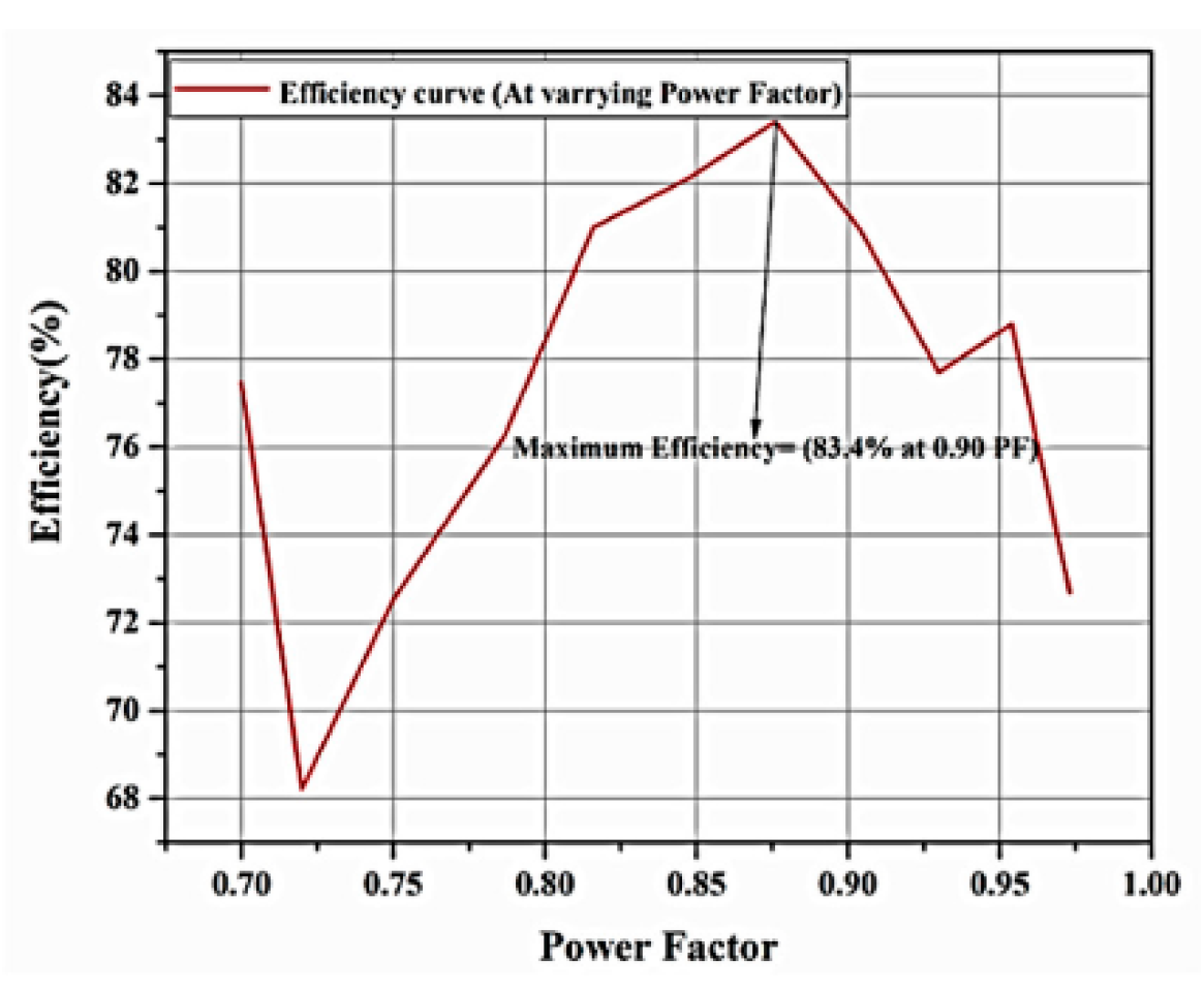
Furthermore, the HS-SZSC interfaced with the 3-phase H-bridge inverter is also tested at different loading as well as power factor conditions which are demonstrated in Figure 17 and Figure 18, respectively. Figure 17 shows the variation in the efficiency with the load current (at unity power factor).
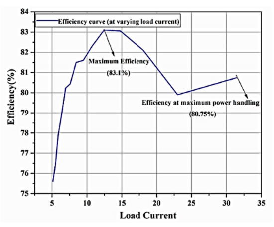
Figure 17.
Efficiency vs. load current (at different loading conditions).

Figure 18.
Efficiency vs. power factor.
The efficiency of the inverter at maximum power handling is 80.75; however, it can achieve the maximum efficiency of 83.1%. The efficiency vs. power factor graph is shown in Figure 18. The efficiency of the proposed design varies with variations in the power factor; however, the maximum efficiency that can be achieved is 83.4% at 0.90 pf lagging. Owing to the gain ability and flexibility in the control of switched converter, it is observed that the proposed design is more suitable for interfacing RESs with the AC grid.
7. Conclusions and Future Works
In this work, an advanced model of the Z-source converter (HS-SZSC) intended for the GCI application is investigated. The proposed model exhibits the features of a higher boost factor and utilizes a reduced number of components thus making it cost-effective and highly efficient. In addition, the performance of the HS-SZSC employed with a GCI is analyzed and compared with conventional ZSC for both normal and transient conditions. In comparison to the ZSC, the proposed HS-SZSC performs better in both conditions. During the normal condition, the HS-SZSC attained a higher boost factor of 4.28 and the smaller THD value of 0.55% which complies well with the IEEE standards. Besides, during the transient condition, it maintained the constant output voltage throughout the variations in the input voltage. Apart from that, this paper also suggests a Simulink model to address the islanding issue GCIs. Finally, the HS-SZSC interfaced with the 3-phase inverter was tested under varying load conditions (at unity power factor) and power factor conditions. The two-stage conversion system utilizing a switched converter maintained the efficiency of 80.75% at maximum power handling and maximum efficiency of 83.6%. Owing to the performance of the HS-SZSC in normal and transient conditions, it can be concluded that the proposed HS-SZSC is more suitable for GCI applications. Future work will involve practical validation of the proposed design. Later on, the proposed design will also be used for single stage power conversion employed with a self-boost ability.
Author Contributions
Conceptualization, R.K. (Rahul Kumar) and R.K. (Ramani Kannan); methodology, R.K. (Rahul Kumar) and N.S.S.S.; GMA software, R.K. (Rahul Kumar); validation, G.E.M.A., M.B. and N.M.; formal analysis, R.K. (Ramani Kannan); investigation, N.S.S.S.; resources, N.S.S.S. and N.M.; data curation, G.E.M.A. and M.B.; writing—original draft preparation, R.K. (Rahul Kumar); writing—review and editing, R.K. (Ramani Kannan) and G.E.M.A.; visualization, R.K. (Ramani Kannan) and N.M.; supervision, R.K. (Ramani Kannan); project administration, R.K. (Ramani Kannan) and R.K. (Rahul Kumar); funding acquisition, N.S.S.S. and N.M. All authors have read and agreed to the published version of the manuscript.
Funding
This research has been sponsored by INTI International University, Malaysia in terms of software simulation and sponsoring this research work from beginning till publication.
Acknowledgments
The author wishes to extend his sincere thanks to the support of Centre of Graduate Studies, Universiti Teknologi, PETRONAS, Malaysia and Faculty of Data Science and Information Technology, INTI International University, Malaysia for providing the state-of-the-art research facilities to carry on this work. In addition to this, the author is also thankful for the support provided by the collaborators from Condition Monitoring System, National Centre of Robotics and Automation, Mehran University of Engineering and Technology, Jamshoro, Sindh Pakistan. The entire project had been sponsored by the Faculty of Data Science and Information Technology, INTI International University, Malaysia for necessary results.
Conflicts of Interest
The authors declare no conflict of interest.
References
- Revathi, B.S.; Prabhakar, M.; Gonzalez-Longatt, F. High-gain–high-power (HGHP) DC-DC converter for DC microgrid applications: Design and testing. Int. Trans. Electr. Energy Syst. 2018, 28, 1–45. [Google Scholar] [CrossRef] [Green Version]
- Kuang, Y.; Zhang, Y.; Zhou, B.; Li, C.; Cao, Y.; Li, L.; Zeng, L. A review of renewable energy utilization in islands. Renew. Sustain. Energy Rev. 2016, 59, 504–513. [Google Scholar] [CrossRef]
- Akinyele, D.O.; Rayudu, R.K.; Nair, N.K.C. Global progress in photovoltaic technologies and the scenario of development of solar panel plant and module performance estimation—Application in Nigeria. Renew. Sustain. Energy Rev. 2015, 48, 112–139. [Google Scholar] [CrossRef]
- Prabaharan, N.; Palanisamy, K. Analysis and integration of multilevel inverter configuration with boost converters in a photovoltaic system. Energy Convers. Manag. 2016, 128, 327–342. [Google Scholar] [CrossRef]
- Syam, M.S.; Kailas, T.S. Grid connected PV system using Cuk converter. In Proceedings of the 2013 Annual International Conference on Emerging Research Areas and 2013 International Conference on Microelectronics, Communications and Renewable Energy, Kanjirapally, India, 4–6 June 2013. [Google Scholar] [CrossRef]
- Sener, E.; Ertasgin, G. A 3-ph Grid-Connected Photovoltaic Inverter Utilizing Super-Lift Luo Converter. In Proceedings of the 2018 2nd International Symposium on Multidisciplinary Studies and Innovative Technologies (ISMSIT), Ankara, Turkey, 19–21 October 2018; pp. 1–5. [Google Scholar] [CrossRef]
- Li, W.; He, X. Review of nonisolated high-step-up DC/DC converters in photovoltaic grid-connected applications. IEEE Trans. Ind. Electron. 2011, 58, 1239–1250. [Google Scholar] [CrossRef]
- Kim, J.K.; Moon, G.W. Derivation, analysis, and comparison of nonisolated single-switch high step-up converters with low voltage stress. IEEE Trans. Power Electron. 2015, 30, 1336–1344. [Google Scholar] [CrossRef]
- Choi, W.Y.; Lee, C.G. Photovoltaic panel integrated power conditioning system using a high efficiency step-up DC-DC converter. Renew. Energy 2012, 41, 227–234. [Google Scholar] [CrossRef]
- Wu, G.; Ruan, X.; Ye, Z. Nonisolated High Step-Up DC—DC Converters. IEEE Trans. Ind. Electron. 2015, 62, 383–393. [Google Scholar] [CrossRef]
- Poorali, B.; Torkan, A.; Adib, E. High step-up Z-source DC-DC converter with coupled inductors and switched capacitor cell. IET Power Electron. 2015, 8, 1394–1402. [Google Scholar] [CrossRef]
- Stauth, J.T. Pathways to mm-scale DC-DC converters: Trends, opportunities, and limitations. In Proceedings of the 2018 IEEE Custom Integrated Circuits Conference, CICC 2018, San Diego, CA, USA, 8–11 April 2018; pp. 1–8. [Google Scholar] [CrossRef]
- Ballo, A.; Grasso, A.D.; Palumbo, G. Current-mode body-biased switch to increase performance of linear charge pumps. Int. J. Circuit Theory Appl. 2020, 48, 1864–1872. [Google Scholar] [CrossRef]
- Stauth, J.T.; Seeman, M.D.; Kesarwani, K. Resonant switched-capacitor converters for sub-module distributed photovoltaic power management. IEEE Trans. Power Electron. 2013, 28, 1189–1198. [Google Scholar] [CrossRef]
- Ballo, A.; Bottaro, M.; Grasso, A.D.; Palumbo, G. Regulated charge pumps: A comparative study by means of verilog-AMS. Electronics 2020, 9, 998. [Google Scholar] [CrossRef]
- Ballo, A.; Grasso, A.D.; Palumbo, G.; Tanzawa, T. Linear distribution of capacitance in Dickson charge pumps to reduce rise time. Int. J. Circuit Theory Appl. 2020, 48, 555–566. [Google Scholar] [CrossRef]
- Shams, I.; Mekhilef, S.; Tey, K.S. Advancement of voltage equalizer topologies for serially connected solar modules as partial shading mitigation technique: A comprehensive review. J. Clean. Prod. 2021, 285, 124824. [Google Scholar] [CrossRef]
- Ajami, A.; Ardi, H.; Farakhor, A. A Novel High Step-up DC/DC Converter Based on Integrating Coupled Inductor and Switched-Capacitor Techniques for Renewable Energy Applications. IEEE Trans. Power Electron. 2015, 30, 4255–4263. [Google Scholar] [CrossRef]
- Tang, Y.; Fu, D.; Wang, T.; Xu, Z. Hybrid switched-inductor converters for high step-up conversion. IEEE Trans. Ind. Electron. 2015, 62, 1480–1490. [Google Scholar] [CrossRef]
- Changchien, S.K.; Liang, T.J.; Chen, J.F.; Yang, L.S. Step-up DC-DC converter by coupled inductor and voltage-lift technique. IET Power Electron. 2010, 3, 369–378. [Google Scholar] [CrossRef] [Green Version]
- Sizkoohi, H.M.; Milimonfared, J.; Taheri, M.; Salehi, S. High step-up soft-switched dual-boost coupled-inductor-based converter integrating multipurpose coupled inductors with capacitor-diode stages. IET Power Electron. 2015, 8, 1786–1797. [Google Scholar] [CrossRef]
- Hu, X.; Gong, C. A high voltage gain DC-DC converter integrating coupled-inductor and diode-capacitor techniques. IEEE Trans. Power Electron. 2014, 29, 789–800. [Google Scholar] [CrossRef]
- Young, C.M.; Wu, S.F.; Chen, M.H.; Chen, S.J. Single-phase ac to high-voltage dc converter with soft-switching and diode-capacitor voltage multiplier. IET Power Electron. 2014, 7, 1704–1713. [Google Scholar] [CrossRef]
- Liang, T.J.; Chen, S.M.; Yang, L.S.; Chen, J.F.; Ioinovici, A. Ultra-large gain step-up switched-capacitor DC-DC converter with coupled inductor for alternative sources of energy. IEEE Trans. Circuits Syst. I Regul. Pap. 2012, 59, 864–874. [Google Scholar] [CrossRef]
- Saravanan, S.; Babu, N.R. Analysis and implementation of high step-up DC-DC converter for PV based grid application. Appl. Energy 2017, 190, 64–72. [Google Scholar] [CrossRef]
- Peng, F.Z. Z-source inverter. IEEE Trans. Ind. Appl. 2003, 39, 504–510. [Google Scholar] [CrossRef]
- Evran, F.; Aydemir, M.T. Z-source-based isolated high step-up converter. IET Power Electron. 2013, 6, 117–124. [Google Scholar] [CrossRef]
- Sharifi, S.; Monfared, M. Modified Series and Tapped Switched-Coupled-Inductors Quasi-Z-Source Networks. IEEE Trans. Ind. Electron. 2019, 66, 5970–5978. [Google Scholar] [CrossRef]
- Zhang, G.; Zhang, B.; Li, Z.; Qiu, D.; Yang, L.; Halang, W.A. A 3-Z-network boost converter. IEEE Trans. Ind. Electron. 2015, 62, 278–288. [Google Scholar] [CrossRef]
- Torkan, A.; Ehsani, M. A Novel Nonisolated Z-Source DC-DC Converter for Photovoltaic Applications. IEEE Trans. Ind. Appl. 2018, 54, 4574–4583. [Google Scholar] [CrossRef]
- Krishna, M.V.; Varma, L.T.V.; Kumar, M.A. Simulation Of High Step up Z-Source DC-DC Converter With Voltage Multiplier Using Coupled Inductors. IJRAR-Int. J. Res. Anal. Rev. 2018, 5, 594–598. [Google Scholar]
- MHaji-Esmaeili, M.; Babaei, E.; Sabahi, M. High Step-Up Quasi-Z Source DC-DC Converter. IEEE Trans. Power Electron. 2018, 33, 10563–10571. [Google Scholar] [CrossRef]
- Shen, H.; Zhang, B.; Qiu, D. Hybrid Z-Source Boost DC-DC Converters. IEEE Trans. Ind. Electron. 2017, 64, 310–319. [Google Scholar] [CrossRef]
- Zhang, G.; Iu, H.H.-C.; Zhang, B.; Li, Z.; Fernando, T.; Chen, S.-Z.; Zhang, Y. An Impedance Network Boost Converter with a High-Voltage Gain. IEEE Trans. Power Electron. 2017, 32, 6661–6665. [Google Scholar] [CrossRef]
- Florescu, A.; Stocklosa, O.; Teodorescu, M.; Radoi, C.; Stoichescu, D.A.; Rosu, S. The advantages, limitations and disadvantages of Z-source inverter. Proc. Int. Semicond. Conf. CAS 2010, 2, 483–486. [Google Scholar] [CrossRef]
- Subhani, N.; Kannan, R.; Porkumaran, K.; Prasath, S.; Srinath, M. An Improved Modified Capacitor-Assisted Z-Source Inverter with Reduced Capacitor Voltage Stress and Inrush Start-up Current. In Proceedings of the 2019 IEEE Conference on Energy Conversion (CENCON), Yogyakarta, Indonesia, 16–17 October 2019; pp. 182–187. [Google Scholar] [CrossRef]
- Subhani, N.; Kannan, R.; Mahmud, A. New Symmetric Enhanced-Boost Modified Z-Source Inverters with Switched Z-Impedance. In Proceedings of the 2020 IEEE International Conference on Power Electronics, Smart Grid and Renewable Energy (PESGRE2020), Cochin, India, 2–4 January 2020; pp. 1–6. [Google Scholar] [CrossRef]
- Kumar, R.; Kannan, R.; Nor, N.B.M.; Mahmud, A. A high step-up switched z-source converter (Hs-szc) with minimal components count for enhancing voltage gain. Electronics 2021, 10, 924. [Google Scholar] [CrossRef]
- Kumar, R.; Kannan, R.; Bin, N.; Nor, M. A High Gain Switched Z-Source Converter with Reduced Passive Components. Solid State Technol. 2020, 63, 4160–4170. [Google Scholar]
- Kandasamy, K.V. Regulated DC-DC Converter for Grid Connected System during Hazardous Conditions. In Proceedings of the 2017 International Conference on Algorithms, Methodology, Models and Applications in Emerging Tech-nologies (ICAMMAET), Chennai, India, 16–18 February 2017. [Google Scholar]
- Aboadla, E.H.E.; Khan, S.; Habaebi, M.H.; Gunawan, T.; Hamidah, B.A.; Yaacob, M.B. Effect of Modulation Index of Pulse Width Modulation Inverter on Total Harmonic Distortion for Sinusoidal. In Proceedings of the 2016 International Conference on Intelligent Systems Engineering (ICISE), Islamabad, Pakistan, 15–17 January 2016. [Google Scholar]
- Zope, P.H.; Bhangale, P.G.; Sonare, P.; Suralkar, S.R. Design and Implementation of carrier based Sinusoidal PWM Inverter. Int. J. Adv. Res. Electr. Electron. Instrum. Eng. 2012, 1, 230–236. [Google Scholar]
- Ramesh, V.; Latha, Y.K. Performance improvement of grid connected PV system using new converter topologies. In Proceedings of the 2017 2nd IEEE International Conference on Electrical, Computer and Communication Technologies, ICECCT, Tamil Nadu, India, 22–24 February 2017. [Google Scholar] [CrossRef]
- Mawlikar, M.A.; Nair, S.S. A comparative analysis of Z source inverter and DC-DC converter fed VSI. In Proceedings of the 2017 International Conference on Nascent Technologies in Engineering (ICNTE), Vashi, India, 27–28 January 2017; pp. 1–6. [Google Scholar] [CrossRef]


Publisher’s Note: MDPI stays neutral with regard to jurisdictional claims in published maps and institutional affiliations. |
© 2022 by the authors. Licensee MDPI, Basel, Switzerland. This article is an open access article distributed under the terms and conditions of the Creative Commons Attribution (CC BY) license (https://creativecommons.org/licenses/by/4.0/).