Article

Readout Electronics of the Prototype Beam Monitor in the HIRFL-CSR External-Target Experiment

1
Institute of Modern Physics, Chinese Academy of Sciences, Lanzhou 730000, China
2
School of Nuclear Science and Technology, University of Chinese Academy of Sciences, Beijing 100049, China
3
PLAC, Key Laboratory of Quark and Lepton Physics (MOE), Central China Normal University, Wuhan 430079, China
*
Author to whom correspondence should be addressed.
Electronics 2022, 11(17), 2679; https://doi.org/10.3390/electronics11172679
Submission received: 2 August 2022 / Revised: 23 August 2022 / Accepted: 24 August 2022 / Published: 26 August 2022

Abstract

:
The External-target Experiment (CEE) at the Cooling Storage Ring of the Heavy-Ion Research Facility in Lanzhou (HIRFL-CSR) will be the first large-scale experiment in nuclear physics independently developed in China covering the GeV energy regime. The beam monitor located at the center front of the CEE accurately measures the position of the particles with a few tens of um accuracy in a non-interceptive way. This unique advantage significantly improves the accuracy of the particle track reconstructions. This beam monitor’s readout electronics consist of the Front-end module (FEM), Readout Control Module (RCM), and Clock Synchronization module (CSM). Twhe novel Topmetal series pixel sensors directly collect the ionized charge along the track of the ion beam while it passes through the gas in the beam monitor. Lab test proves that the readout electronics have an INL of less than 1%. In addition, the prototype beam monitor can measure the position of the 40Ar beam of 320 MeV/u with a resolution of ~6.9 μm. This paper will discuss the design, characterization, and test of the readout electronics.

1. Introduction

The proposed CSR External-target Experiment (CEE) will be China’s first large-scale experiment to study nuclear physics in the GeV energy region [1,2]. This energy region is well covered by the Cooling Storage Ring of the Heavy-Ion Research Facility in Lanzhou (HIRFL-CSR) [3,4,5]. As a large acceptance spectrometer, the CEE experiment will explore quantum-chromo-dynamics phase structure and equation of state at high-baryon density. Figure 1 shows the overall design of the CEE, which mainly includes the Beam Monitor [6], the Time Projection Chamber (TPC), the Time-of-Flight detector (TOF), the Multi-wire Drift Chamber (MWDC), and the Zero Degree Calorimeter (ZDC) [7].
The beam monitor locates at the center front of the CEE, inside the magnetic shielding tube, about 80 cm away from the collision target. The beam monitor can measure the particle tracks in a non-destructive way with the accuracy of several tens of micrometers. This unique advantage significantly improves the accuracy of the track reconstructions. Figure 2a shows that the beam monitor is a gas drift chamber that uses the Topmetal series CMOS pixel sensors [8,9,10,11] as the charge collection nodes. The basic working principle of the beam monitor is shown in Figure 2b and described below:
(1)
The particles generate electrons by ionizing the gas while it passes through the drift chamber.
(2)
Driven by the electric field in the cages, the ionized electrons drift to the Topmetal CMOS pixel sensors.
(3)
In each pixel, part of the top metal layer, named Topmetal, is exposed to direct collect the drift charge, and the in-pixel charge-sensitive amplifier converts the charge into an electrical signal.
(4)
The charge is reconstructed to extrapolate the particle’s projection in the X-Z and Y-Z planes. Then a 3D beam profile is obtained by combining the two projections.
The total size of the gas chamber is 120 mm × 120 mm × 163 mm, the size of the incident window is 50 mm × 50 mm, and the size of each pixel is about several tens of micrometers. The overall functionality of this beam monitor has been discussed in [6]. This paper focuses on the design of the readout electronics and the heavy-ion beam test.

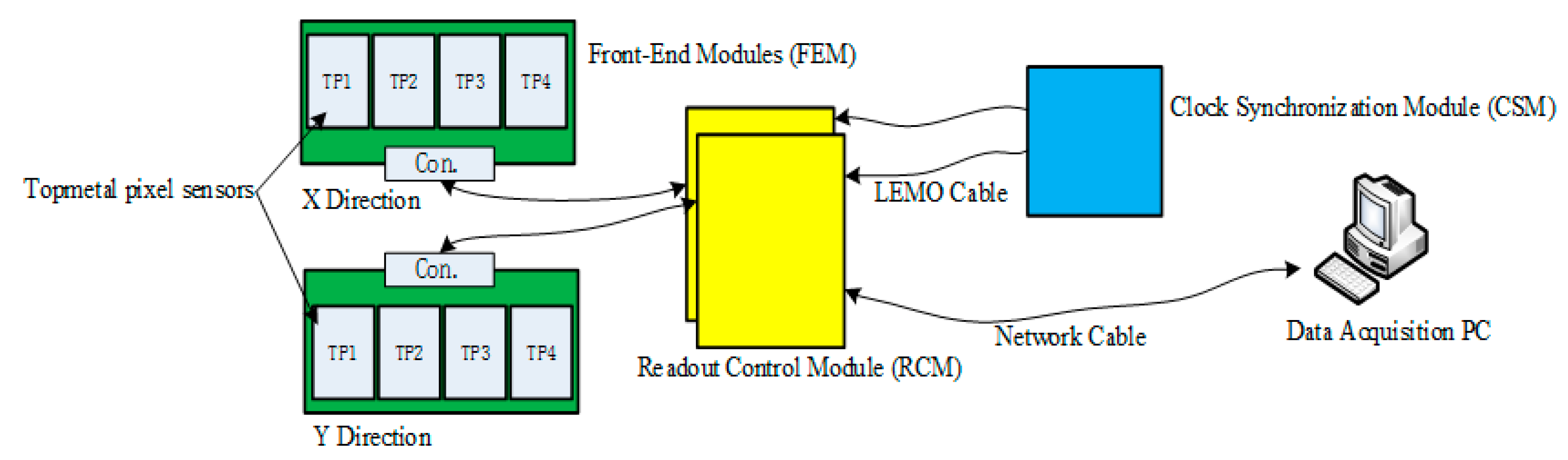
2. Readout Electronics Design

As shown in Figure 3, the readout electronics consist of the Front-End Modules (FEM), the Readout Control Module (RCM), and Clock Synchronization Module (CSM). Each FEM holds four Topmetal CMOS pixel sensors, which directly collect the drift electrons in the gas chamber and convert them into an analog signal. The RCM converts the analog signal from the FEM into a digital one, process it, and transmits it to the Data Acquisition Computer via a Gigabit Ethernet link. The RCMs are connected to the FEMs via flexible printed circuits of 30 cm. In addition, the CSM distributes clock signals from the same source to RCMs, to make the RCMs work synchronously.

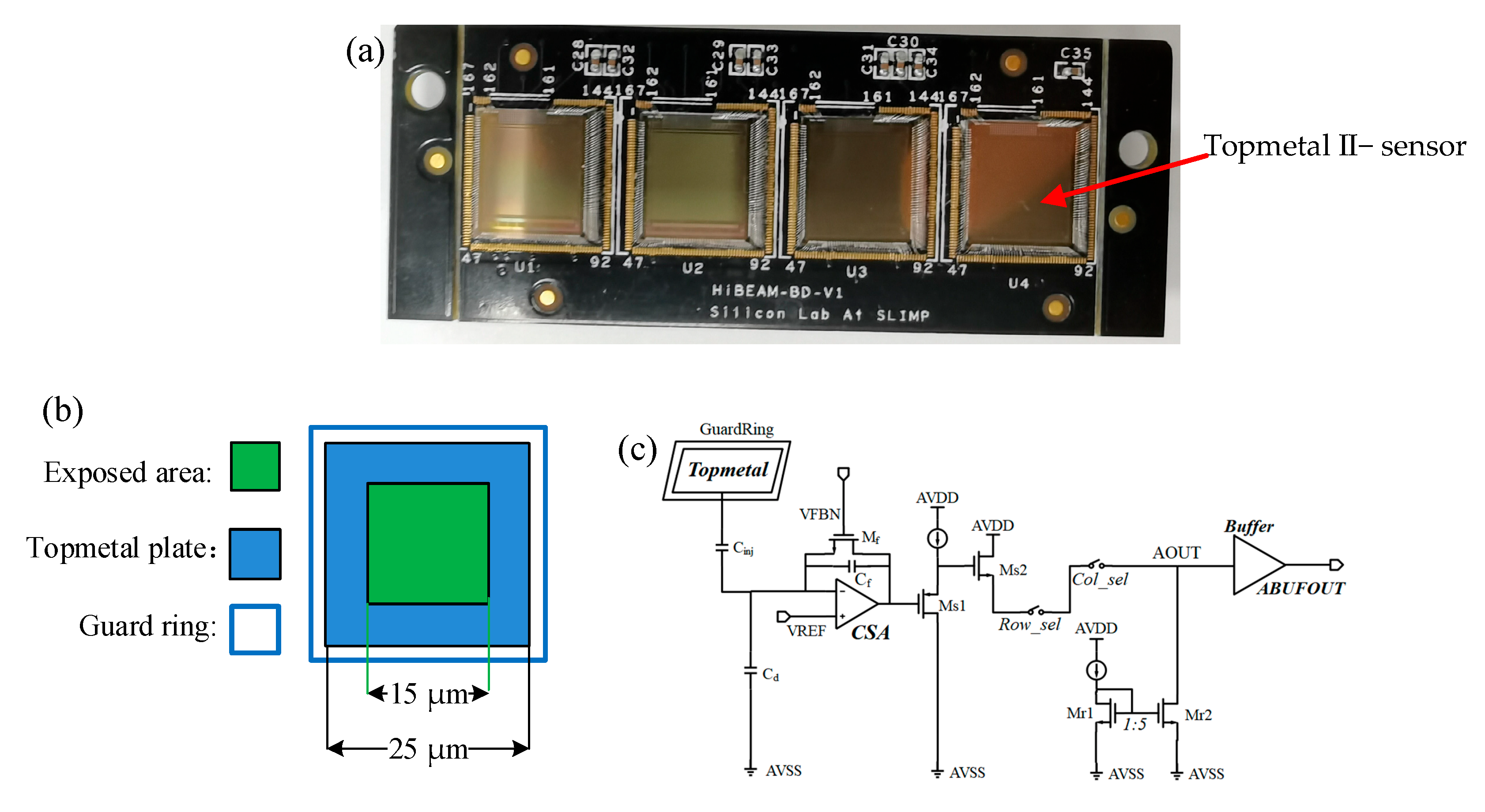
2.1. The Front-End Module

Figure 4a shows the picture of the FEM. The main components of the FEM are the Topmetal II− pixel sensors. Each Topmetal II− has 72 × 72 pixels and the size of each pixel is 83 μm × 83 μm. Figure 4b shows that the total size of the Topmetal plate is 25 µm × 25 µm, and the size of the exposed area is 15 µm × 15 µm. As shown in Figure 4c, the charge collected by the Topmetal plate is converted to a voltage signal by a low-noise charge-sensitive amplifier (CSA) and transmitted via two source-following stages and an analog output buffer [12]. Since the Topmetal plate collects charge directly from the surrounding medium, there is no detector leakage current in the sensor. All 5184 pixels in the Topmetal II− are read in a rolling-shutter scheme. The analog output signal from each Topmetal II− sensor is transmitted to RCM through the flexible PCB. The control signals, the clocks, and the power supply of the Topmetal II− sensors are provided by the RCM [13]. Four fan-out chips (ICS8343AY-01LF) are on the FEM, which fans out different control signals from the RCM to each pixel chip. Several onboard resistors adjust the bias voltage of the Topmetal II− sensors.

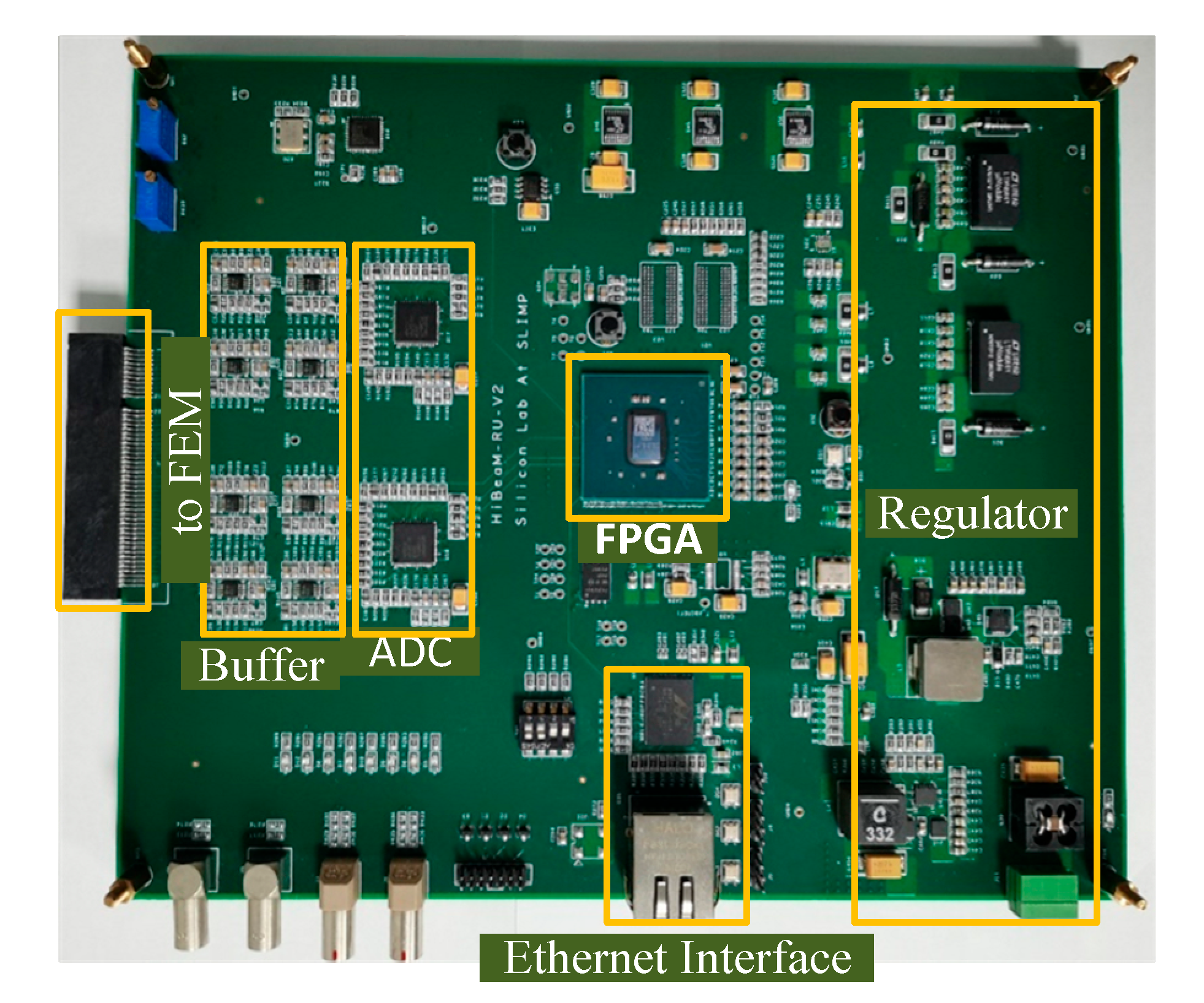
2.2. The Readout Control Module

Figure 5 and Figure 6 show the overview of the RCM design and the picture of the RCM. The RCM mainly consists of the main field-programmable gate array (Xilinx Kintex-7 [14]), the analog buffer circuit, and two high-resolution ADCs (AD9252 [15]), two 16bit-DDR3 memories, the power supply circuit, and the Ethernet Interface.
Each RCM in the beam monitor receives and processes the analog signals from up to four FEMs. In beam monitor, each RCM handles one FEM with four Topmetal II− sensors. On the RCM, the analog signal from the Topmetal II− sensors firstly goes into the analog buffer circuit, which converts the single-ended signal to a differential signal and filters the differential signal. Then the ADCs sample and digitize the differential signal into 14-bits digital data at the frequency of 25 MHz. The Topmetal II− sensors generate analog output at 1.25 MHz. Each analog output is sampled and digitized 20 times by the 25Msps 14-bit ADC. Then the average value of the middle eight samples is calculated. Afterward, the FPGA packs the data with a timestamp and an RCM number and transmits the data packages to the Data Acquisition Computer via 1 Gigabit Ethernet using TCP/IP protocol. At the same time, there is a current-monitoring circuit on the board, which can monitor the current of the Topmetal II− chip in real-time.

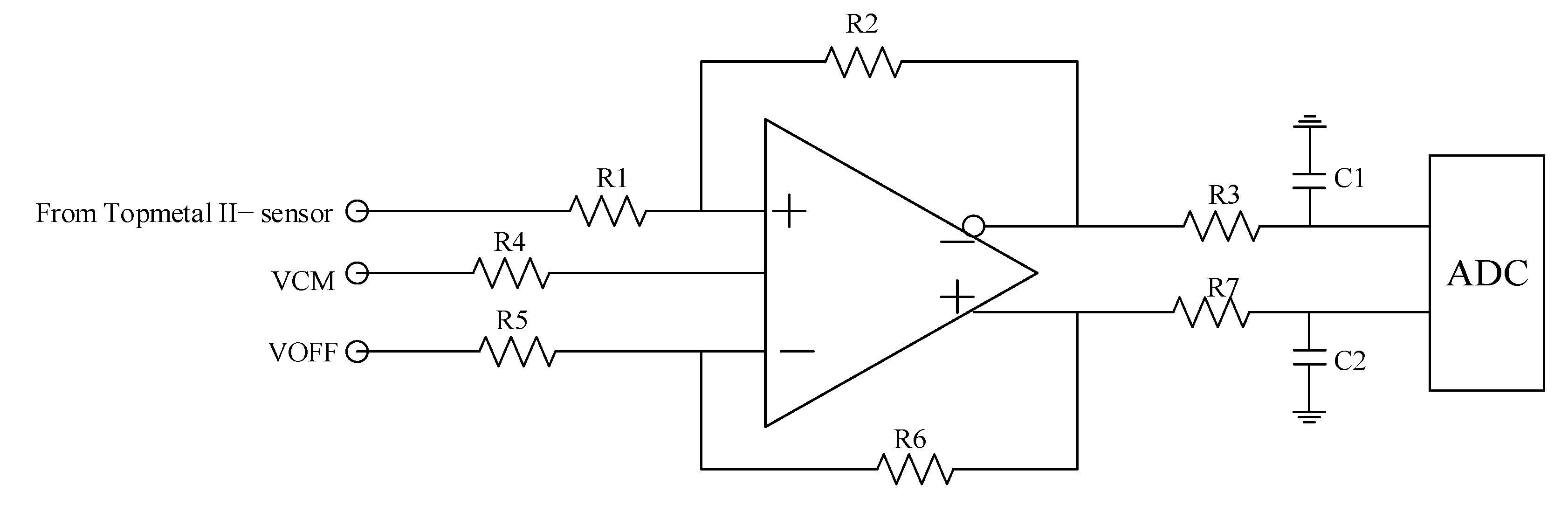
2.2.1. The Analog Buffer Circuit

Figure 7 shows the block diagram of the analog buffer circuit, which consists of an operational amplifier, resistors, and capacitors. This buffer circuit is compulsory since the ADC has no drive and buffer circuits for its input. The operational amplifier is the THS4521 [16] from Texas Instruments, which has high bandwidth and low noise. The resistor network provides the bias voltage (VOFF) to the Topmetal II− sensor to adjust its output baseline. The output common-mode voltage (VCM) of the THS4521 is set as 0.9 V, which matches the ADC input’s common-mode voltage.

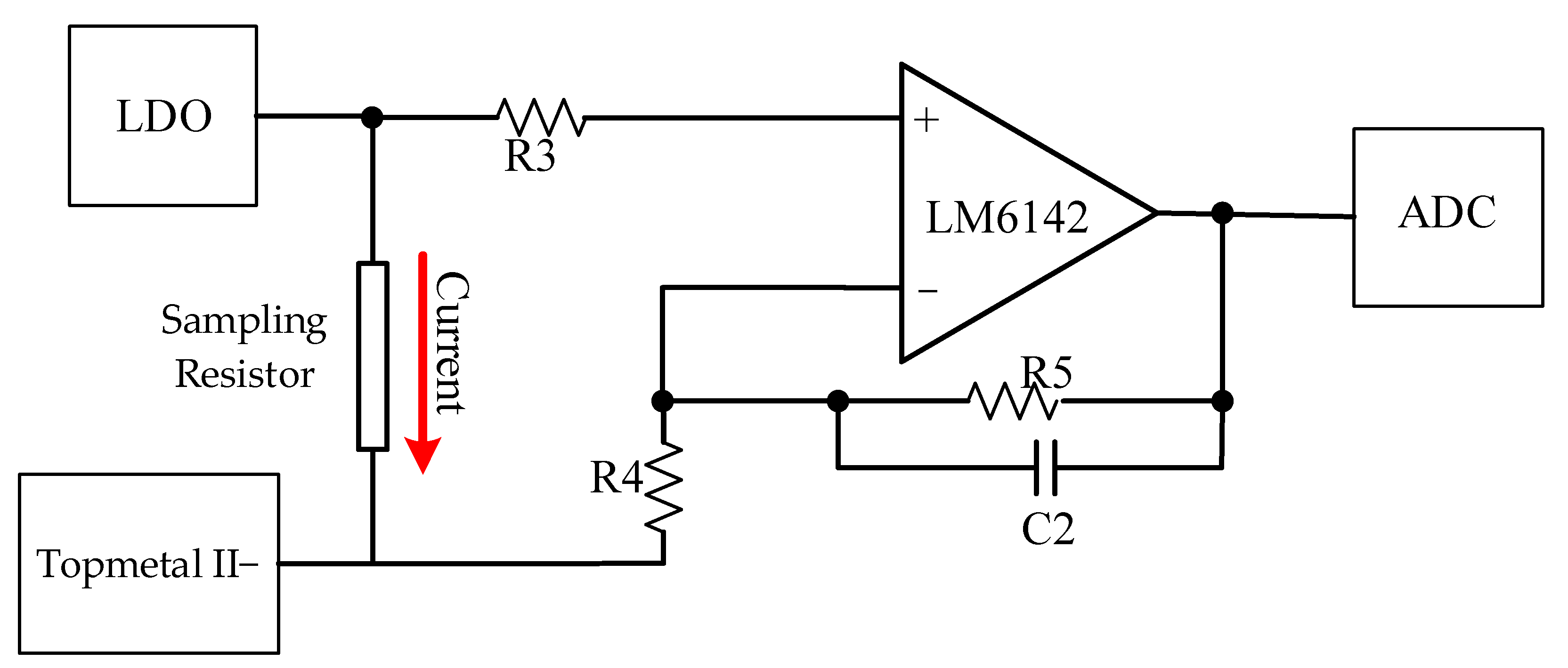
2.2.2. The Current Monitoring Circuit

The current monitoring circuit monitors the current of the digital and analog power supply of the Topmetal II− sensors. Figure 8 shows the current monitoring circuit’s block diagram, consisting of a sampling resistor, an operational amplifier (LM6142), and a multi-channel ADC (TLV2548). The current value is sampled every second. The power supply automatically turns off and turns on after 10 ms if the current exceeds the safe limit of 10 mA. This current monitoring circuit can prevent the Topmetal II− sensors from being burned by the high transient current induced by potential radiation effects [17].

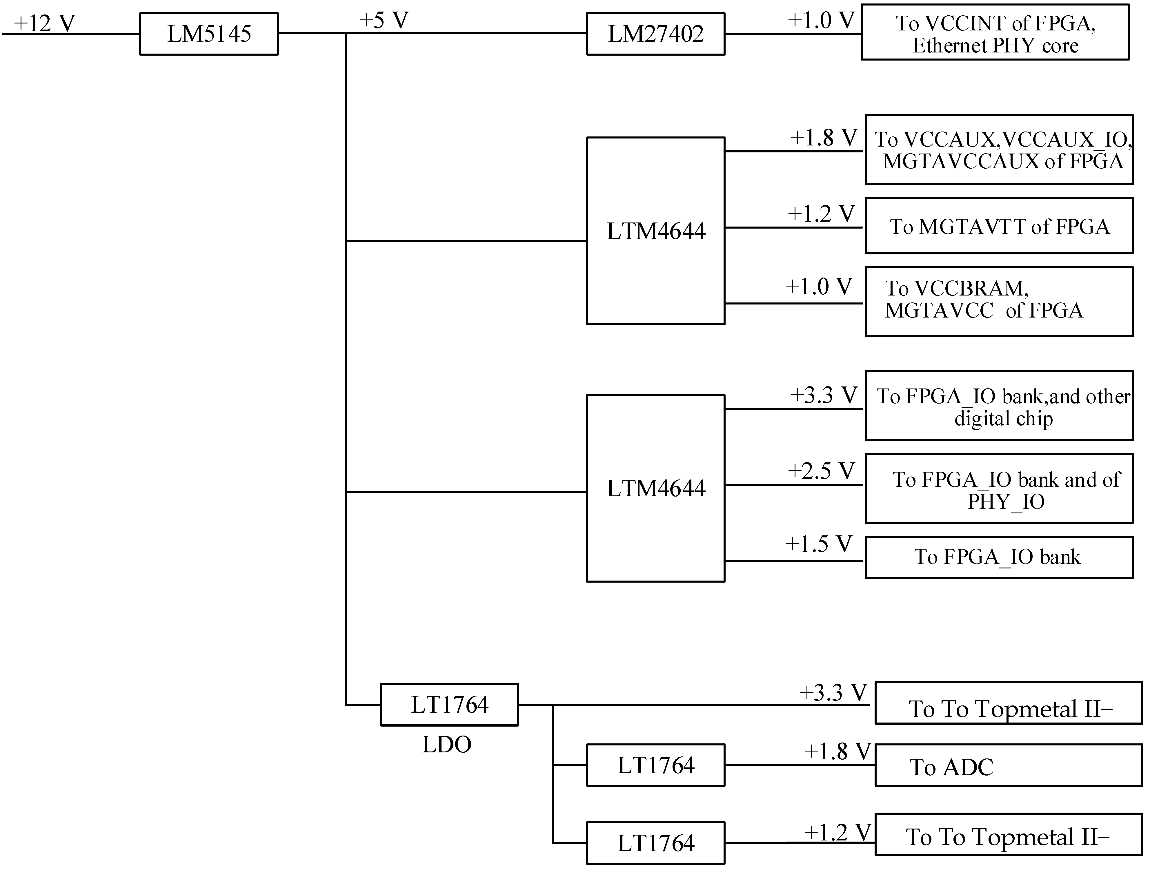
2.2.3. The Power Distribution Network

Figure 9 shows the typology of the power distribution network on the RCM. A set of high-efficient DC-DC chips and low-drop voltage regulators. First, an external power supply of +12 V is provided to the RCM. Then, the DC/DC controller LM5145 generates a +5 V onboard power supply with a high current. Based on this +5 V power supply, a set of DC/DC controllers power the FPGA and other components that are not sensitive to the power noise but require a high drive current. Besides this, a set of Low Drop-Out (LDO) regulators provide the low-ripple bias voltage to the Topmetal II- sensors and the ADCs that are sensitive to power noise.

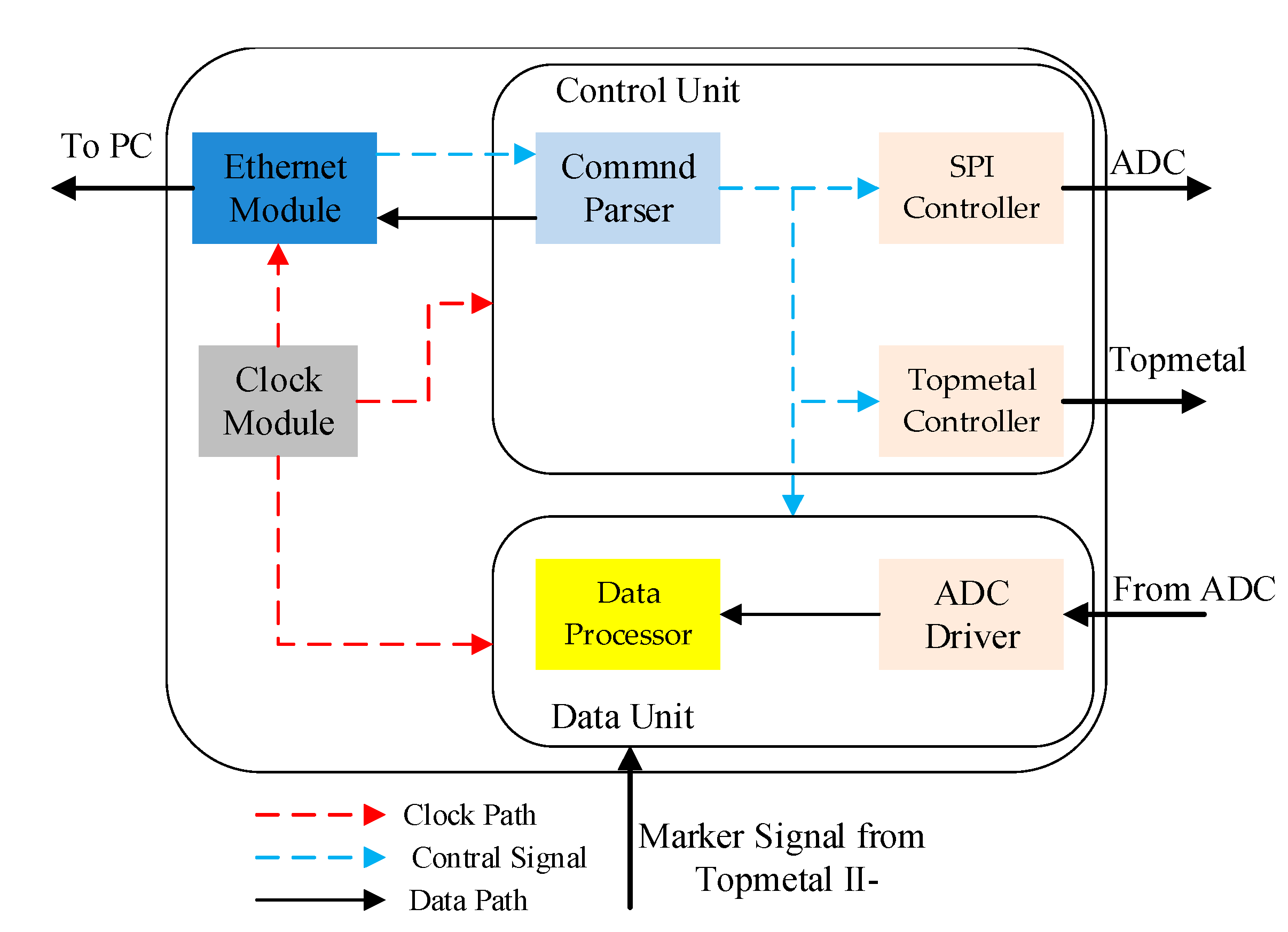
2.2.4. The FPGA Design

Figure 10 shows the block diagram of the FPGA design, which consists of the Gigabit Ethernet Module, the Control Unit, the Data Unit, and the Clock Module. The FPGA is the XC7K70T-2FBG676I from the Xilinx Incorporated [14]. The RCM transmits data to and receives commands from the Data Acquisition Computer (DAQ) through the Gigabit Ethernet Module. The Tri-mode Ethernet MAC [18] is based on an IP core from the Xilinx Cooperation.
The Command Parser in the Control Unit decodes the commands from the DAQ and distributes them into the SPI Controller, the Topmetal Controller, and the Data Unit. The SPI Controller generates the control signals and sends them to the ADC via the SPI bus. The Topmetal Controller generates the control signals for the Topmetal II− chip. In the Data Unit, the ADC Driver converts the 14-bit width parallel data from the ADC into 1-bit width data, aligning with ADC clocks [19]. Then the Data Process Module packages each frame of the ADC data, which starts with the marker signal from the Topmetal II− sensor. The Clock Module distributes a 100 MHz clock to the Control Unit, a 100 MHz clock to the Data Unit, and a 125 MHz clock to the Tri-mode Ethernet MAC. Asynchronous FIFOs between the Data Process Module and Command Parser Module solve the problems of Clock Domain Crossing.

2.3. Clock Synchronization Module

The CSM delivers synchronous clocks and synchronization signals to the RCMs. This scheme is essential to ensure the time synchronization of the data collected from all the FEMs to reconstruct the ion track. Figure 11 shows the block diagram of the CSM, which mainly consists of a 200 MHz crystal oscillator, the clock fanout buffer, the Altera EP3C16F484C8N [20] FPGA, and the UART interface. The clock fanout buffer is IDT8SLVD1208I [21] from Renesas Electronics Corporation can fan out eight channels of high-frequency, very low additive phase-noise differential clocks. In our design, five pairs of clock signals are connected to differential connectors (LEMO standard) and transmitted to the RCMs by LEMO cables. One pair of clock signals is used as the system clock of the Altera FPGA on this CSM. Once the FPGA receives a synchronization command from the DAQ via the RS232 interface, this FPGA will issue five pairs of differential synchronization signals to the RCMs to restart the timestamp count.

2.4. Discussion on Radiation Tolerance

Figure 12 demonstrates the distribution of the secondary radiation dose rate in CEE, which is simulated by bombarding a 238U target with a 1 × 10⁶ pps 238U beam. The energy of the 238U is 500 MeV/u, and the target’s radius and thickness are 4 mm. The FEM locates inside the radiation area with a strong dose rate of ~3 Gy/hour. However, the radiation issue is not a big concern for the FEM. On the one hand, the FEM does not interact with the beam. On the other hand, each pixel in the Topmetal II− is surrounded by a guard ring, and all the other components are passive. These features significantly avoid single event effects and reduce the accumulated dose.

3. Performance Measurement

To evaluate the function and performance of the readout electronics, we have conducted a series of tests.

3.1. Characterization of the Readout Electronics in the Lab

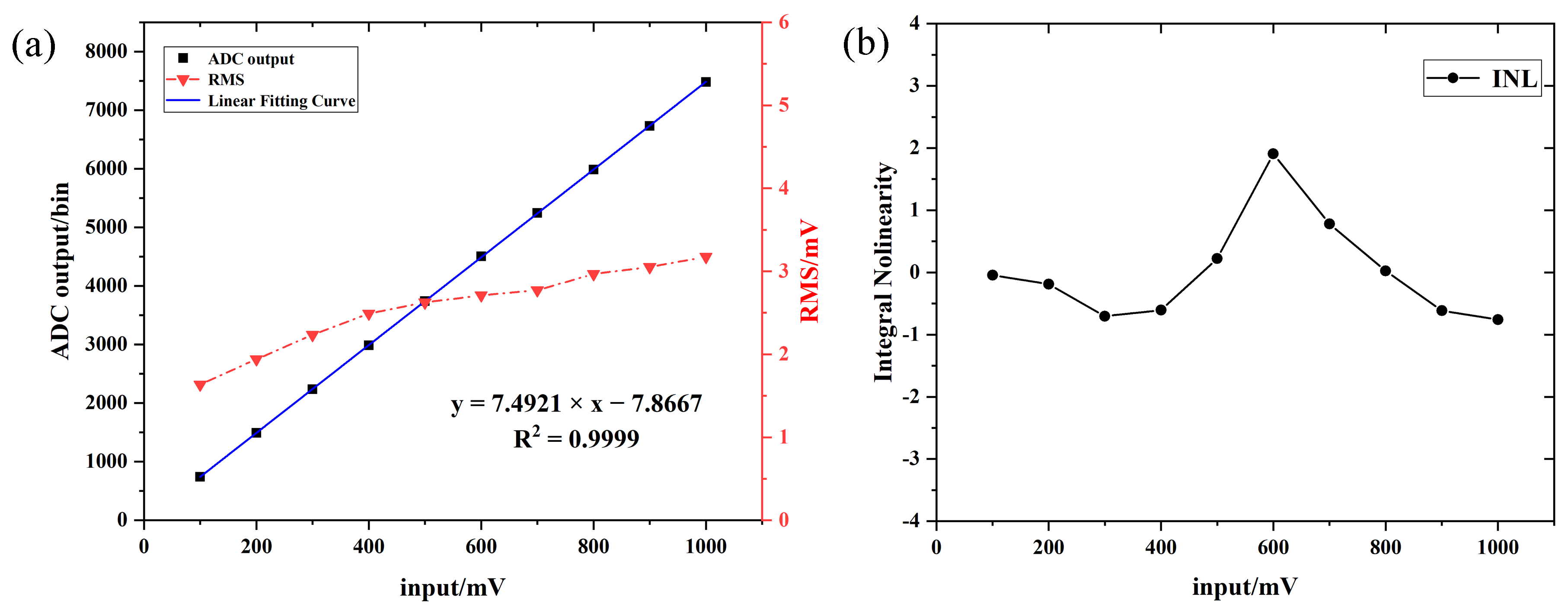
3.1.1. Linearity of the RCM

A test platform was built in the lab to evaluate the RCM’s linearity. In the test, a precise pulse generator (Tektronix AFG3252C [22]) provides input to the RCM, and the RCM is connected to the DAQ through a Gigabit Ethernet cable. The input signal varies from 0.1 V to 1 V in the step of 100 mV. Figure 13a shows the linear function fitted with the output and the corresponding input of the RCM. The average RMS noise is less than three mV. Figure 13b shows the integral nonlinearity (INL) with each specific input value. The maximum INL is about two mV, corresponding to 0.2%.

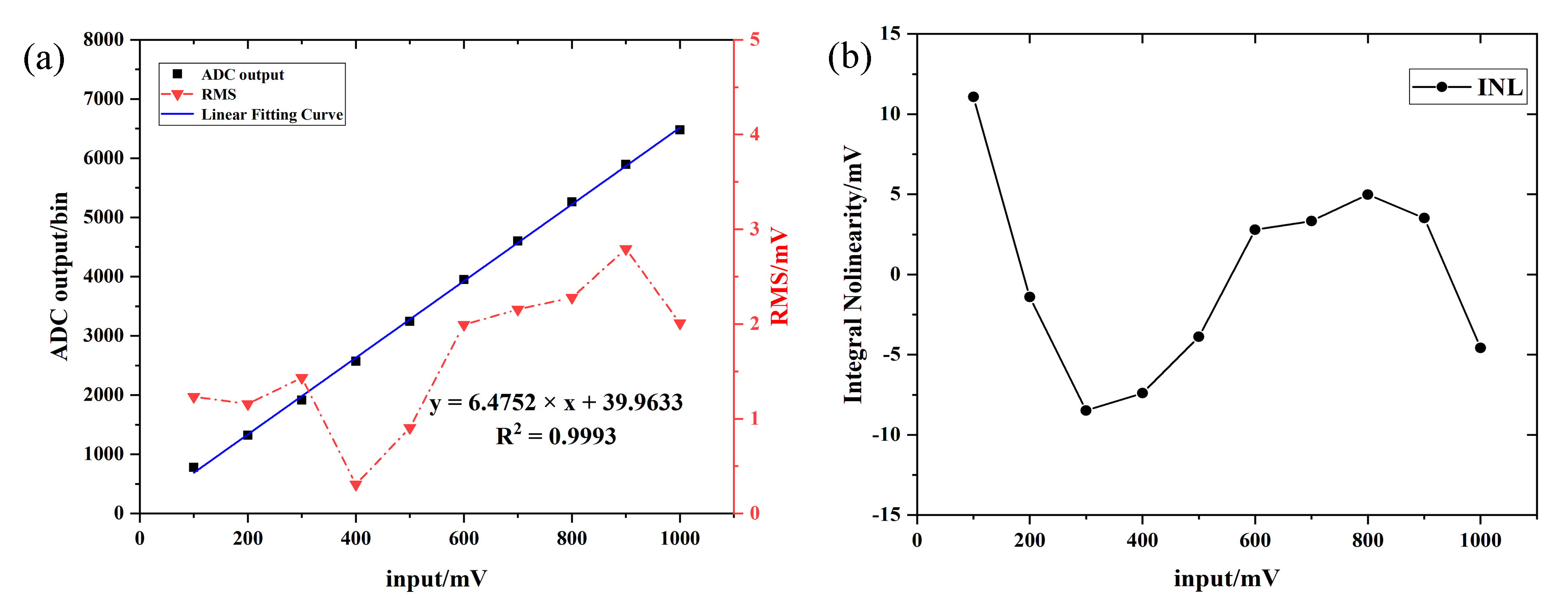
3.1.2. Performance of the Entire Readout Electronics

The linearity of the entire readout chain has been tested. The readout chain consists of the FEM, the RCM, the CSM, and the DAQ. First, an input voltage on the guarding ring injects a test charge to each pixel in the Topmetal II− sensors. Then the test charge is processed and recorded by the readout chain. The input voltage varies from 0.1 V to 1 V with a step of 100 mV. Figure 14a shows the linear function fitted with the recorded output and the corresponding input, and the average RMS noise is less than 3.5 mV. Figure 14b shows the integral nonlinearity (INL) on the output for the different input values. The maximum INL is about 10 mV.
Stability on data readout has been performed on the entire readout system. The precise pulse generator (Tektronix AFG3252C) provides input to the readout system, which keeps working continuously for 72 h. The system runs stably without any stop in the test. The above tests have proved that the readout electronics have good linearity and stable performance.

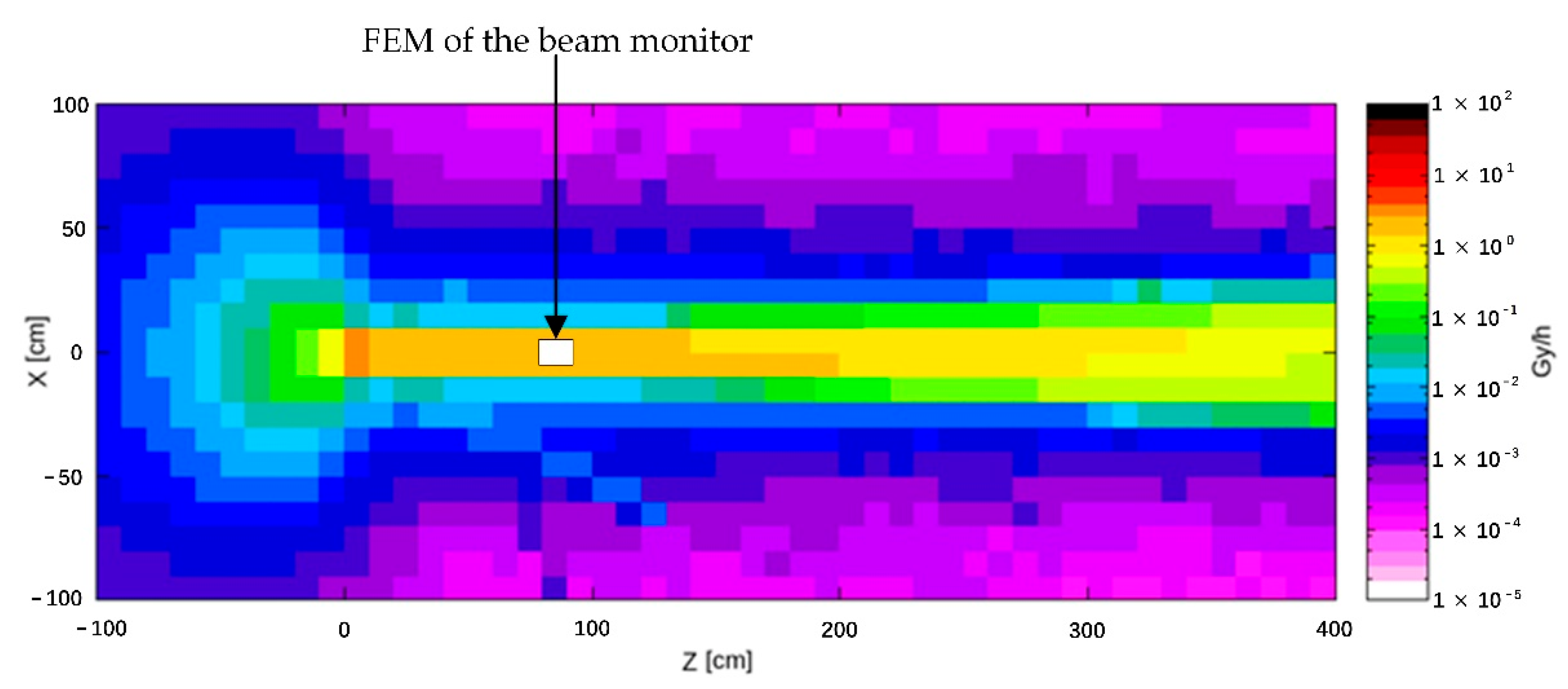
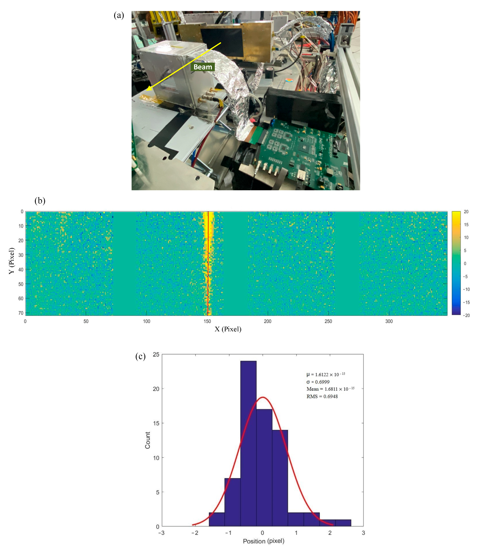
3.2. System Test with Beam

A heavy-ion beam test on this beam monitor is carried out at the Heavy Ion Research Facility in Lanzhou–Cooler Storage Ring (HIRFL-CSR) [23,24]. Figure 15a shows the test setup, in which the whole beam monitor consists of the gas chamber and the readout electronics. Before the beam test, this prototype beam monitor worked stably for 24 h in the lab. First, a uniform continuous 40Ar beam with the Ø of 10 mm and the energy of 320 MeV/u passes through the gas chamber and generates the electrons by ionization. Then, a −35 V/mm electric field applied to the field cage drives the electrons to the Topmetal II− sensors. Figure 15b shows an example of the measured 40Ar beam track (yellow line). The value of each pixel subtracts its average baseline, and then all values of the pixels in each column are summed to form a one-dimensional distribution. The full width at half maximum of this distribution sets the boundary of the track. Then the center of mass of each pixel column along this track within the boundary is calculated and fitted with the least square method (red line). The distance between the center of gravity and the fitted track in each row, defined as Δ P i , forms the distribution in Figure 15c. This distribution’s Root Mean Square (RMS) indicates a single row’s position resolution to measure the heavy ion particle’s track is about 58 μm. The standard error (SE) of the mean ( Δ P ¯ ) of all the rows is calculated to be 6.9 μm with the following equation [8] and represents the spatial resolution of the whole beam monitor to measure the ion track.
P r e s o = 1 n ( n 1 ) i = 1 n ( Δ P i Δ P ¯ ) 2
Hence, the readout electronics of this beam monitor can work fine in beam conditions.

4. Conclusions

The beam monitor of the HIRFL-CSR External-target Experiment monitors the heavy-ion particle tracks in a non-interceptive way. This paper discusses the design, characterization, and test of the beam monitor’s readout electronics. The FEM holds the Topmetal II− pixel sensors to collect the ionized charge by the heavy-ion particle in the gas chamber. The RCM receives the signal from FEM, processes it mainly with the onboard ADCs and FPGA, then transmits it to the DAQ through gigabit Ethernet. Besides this, the CSM distributes synchronous clock signals and synchronization signals to the readout electronics. The lab tests show that the entire readout electronic chain works stably, and the integral non-linearity is less than 1%. In addition, a heavy-ion campaign shows that this prototype beam monitor, including the gas chamber and the readout electronics, measures the 40Ar with 320 MeV/u with an accuracy of ~6.9 μm. Therefore, this beam monitor can provide an accurate vertex for the heavy-ion collision.

Author Contributions

Conceptualization, H.Y. and J.L.; methodology, H.Y. and J.L.; software, H.W. and H.Z.; validation, H.W.; formal analysis, H.W. and W.S.; investigation, H.Y.; resources, C.G.; data curation, J.L.; writing—original draft preparation, H.Y.; writing—review and editing, C.Z.; visualization, X.L.; supervision, C.Z.; project administration, C.G. and C.Z.; funding acquisition, C.G. and C.Z. All authors have read and agreed to the published version of the manuscript.

Funding

This work is supported by the National Natural Science Foundation of China (U2032209, 11975292, 11875304, 12005278, 12005276, 12005279), the CAS “Light of West China” Program, the CAS Pioneer Hundred Talent Program, the Guangdong Major Project of Basic and Applied Basic Research (2020B0301030008), and the Guangdong Laboratory of Advanced Energy Science and Technology.

Institutional Review Board Statement

Not applicable.

Informed Consent Statement

Not applicable.

Data Availability Statement

Not applicable.

Acknowledgments

Special appreciation goes to Yang Li from the Institute of Modern Physics, Chinese Academy of Sciences, for providing the radiation environment simulation of the CEE facility.

Conflicts of Interest

The authors declare no conflict of interest.

References

  1. Yi, H.; Zhao, Z.; Xiao, Z.G.; Cheng, W.; Lü, L.M.; Yan, W.; Wang, R.; Li, H.J.; Huang, Y.; Zhang, Y.; et al. Prototype studies on the forward MWDC tracking array of the external target experiment at HIRFL-CSR. Chin. Phys. C 2014, 38, 126002. [Google Scholar] [CrossRef]
  2. Lü, L.M.; Yi, H.; Xiao, Z.G.; Shao, M.; Zhang, S.; Xiao, G.Q.; Xu, N. Conceptual design of the HIRFL-CSR external-target experiment. Sci. China Phys. Mech. 2017, 60, 012021. [Google Scholar] [CrossRef]
  3. Hu, D.D.; Lu, J.M.; Zhou, J.; Deng, P.P.; Shao, M.; Sun, Y.J.; Zhao, L.; Chen, H.F.; Li, C.; Tang, Z.B.; et al. Extensive beam test study of prototype MRPCs for the T0 detector at the CSR external-target experiment. Eur. Phys. J. C 2020, 80, 282. [Google Scholar] [CrossRef]
  4. Zhan, W.L.; Sun, Z.Y.; Xiao, G.Q.; Xia, J.W.; Zhao, H.W.; Song, M.T.; Yuan, Y.J.; HIRFL-CSR Group. Present status of HIRFL in Lanzhou. Int. J. Mod. Phys. E 2006, 15, 1941–1956. [Google Scholar] [CrossRef]
  5. Xia, J.W.; Zhan, W.L.; Wei, B.W.; Yun, Y.J.; Yuan, P.; Qiao, W.M.; Gao, D.Q.; Yang, X.T.; Man, K.D.; Xiao, G.Q.; et al. HIRFL-CSR complex. Chin. Phys. C 2009, 33, 804. [Google Scholar]
  6. Wang, H.L.; Wang, Z.; Gao, C.S.; Liao, J.W.; Sun, X.M.; Yang, H.B.; Zhao, C.X.; Liu, J.; Ma, P.; Li, Z.L.; et al. Design and tests of the prototype beam monitor of the CSR external target experiment. Nucl. Sci. Tech. 2022, 33, 36. [Google Scholar] [CrossRef]
  7. Zhan, W.L.; Xu, H.S.; Xiao, G.Q.; Xia, J.W.; Zhao, H.W.; Yuan, Y.J. HIRFL-CSR Group Progress in HIRFL-CSR. Nucl. Phys. A 2010, 834, 694c–700c. [Google Scholar] [CrossRef]
  8. Fan, Y.; Gao, C.S.; Huang, G.M.; Li, X.T.; Mei, Y.; Pei, H.; Sun, Q.; Sun, X.M.; Wang, D.; Wang, Z.; et al. Development of a highly pixelated direct charge sensor, Topmetal-I, for ionizing radiation imaging. arXiv 2014, arXiv:1407.3712. [Google Scholar]
  9. Yang, H.B.; Zhang, H.L.; Gao, G.S.; Wang, H.L.; Sun, X.M.; Liu, J.; Wang, S.; Li, X.Q.; Ren, W.P.; Zhou, W.; et al. Hi’Beam-S: A Monolithic Silicon Pixel Sensor-Based Prototype Particle Tracking System for HIAF. IEEE Trans. Nucl. Sci. 2021, 68, 2794–2800. [Google Scholar] [CrossRef]
  10. Yang, H.B.; Mai, F.T.; Liao, J.W.; Zhang, H.L.; Ma, X.M.; Gao, C.S.; Ren, W.P.; Zhou, W.; Sun, X.M.; Liu, J.; et al. Heavy-ion beam test of a monolithic silicon pixel sensor with a new 130 nm High-Resistivity CMOS process. Nucl. Instrum. Meth. A 2022, 1039, 167049. [Google Scholar] [CrossRef]
  11. Ren, W.P.; Zhou, W.; You, B.H.; Fang, N.; Wang, Y.; Yang, H.B.; Zhang, H.L.; Wang, Y.; Liu, j.; Li, X.Q.; et al. Topmetal-M: A novel pixel sensor for compact tracking applications. Nucl. Instrum. Meth. A 2020, 981, 164557. [Google Scholar] [CrossRef]
  12. Gao, G.S.; Huang, G.M.; Sun, X.M. Topmetal II−: A direct charge sensor for high energy physics and imaging applications. JINST 2016, 11, C01053. [Google Scholar] [CrossRef]
  13. Zhang, H.L.; Yang, H.B.; Li, X.Q.; Zhang, Y.Z.; Sun, X.M.; Wang, D.; Huang, R.; Wang, Y.; Zhou, W.; Zhao, C.X. Development of readout electronics a novel beam monitoring system for ion research facility accelerator. arXiv 2020, arXiv:2002.06216. [Google Scholar]
  14. Xilinx Corporation. 7 Series FPGAs Data Sheet: Overview. Available online: https://china.xilinx.com/support/documentation/data_sheets/ds180_7Series_Overview.pdf (accessed on 20 July 2022).
  15. Analog Devices Corporation. Octal, 14-Bit, 50 MSPS, Serial LVDS, 1.8 V ADC-AD9252. Available online: https://www.analog.com/media/en/technical-documentation/data-sheets/AD9252.pdf (accessed on 24 August 2022).
  16. TI Corporation. THS452x Very Low Power, Negative Rail Input, Rail-To-Rail Output, Fully Differential Amplifier. Available online: http://www.ti.com/lit/ds/symlink/ths4521.pdf (accessed on 24 August 2022).
  17. TI Corporation. Single Event Upset and Latchup Considerations for CMOS Devices Operated at 3.3 V. Available online: https://www.ti.com/lit/an/snoa332a/snoa332a.pdf (accessed on 24 August 2022).
  18. Xilinx Corporation. Tri-Mode Ethernet MAC v9.0 LogiCORE IP ProductGuide. Available online: https://www.xilinx.com/content/dam/xilinx/support/documents/ip_documentation/tri_mode_ethernet_mac/v9_0/pg051-tri-mode-eth-mac.pdf (accessed on 20 July 2022).
  19. Zhang, H.L.; Zhang, Y.Z.; Yang, H.B.; Qian, C.; Li, X.Q.; Sun, X.M.; Wang, D.; Huang, R.; Wang, Y.; Zhou, W.; et al. Hi’Beam-A: A Pixelated Beam Monitor for the Accelerator of a Heavy-Ion Therapy Facility. IEEE Trans. Nucl. Sci. 2021, 68, 2081–2087. [Google Scholar] [CrossRef]
  20. Altera Corporation. Cyclone III Device Handbook. Available online: https://www.micro-semiconductor.com/datasheet/99-EP3C5E144I7N.pdf. (accessed on 20 July 2022).
  21. Renesas Electronics Corporation. 1:8, LVDS Output Fanout Buffer-IDT8SLVD1208I Datasheet. Available online: https://www2.renesas.cn/cn/zh/document/dst/idt8slvd1208i-datasheet (accessed on 20 July 2022).
  22. Tektronix. Arbitrary/Function Generator AFG3252 User Guide. Available online: https://www.tek.com/datasheet/afg3000-series (accessed on 20 July 2022).
  23. Yuan, Y.J.; Yang, J.C.; Xia, J.W.; Yuan, P.; Qiao, W.M.; Gao, D.Q.; Xiao, G.Q.; Zhao, H.W.; Xu, H.S.; Song, M.T.; et al. Status of the HIRFL–CSR complex. Nucl. Instrum. Methods Phys. Res. Sect. B 2013, 17, 214. [Google Scholar] [CrossRef]
  24. Xia, J.W.; Zhan, W.L.; Wei, B.W.; Yuan, Y.J.; Song, M.T.; Zhang, W.Z.; Yang, X.D.; Yuan, P.; Gao, D.Q.; Zhao, H.W.; et al. The heavy ion cooler-storage-ring project (HIRFL-CSR) at Lanzhou. Nucl. Instrum. Methods Phys. Res. Sect. A 2002, 488, 11. [Google Scholar] [CrossRef]
Figure 1. Primary detectors of the CEE [6].
Electronics 11 02679 g001
Figure 2. (a) Structure of the beam monitor [6]. (b) Working principle of the beam monitor.
Electronics 11 02679 g002
Figure 3. The architecture of the prototype readout electronics.
Electronics 11 02679 g003
Figure 4. (a) Picture of the FEM. (b) The Topmetal plate’s structure of each pixel. (c) Signal path in the Topmetal II−.
Electronics 11 02679 g004
Figure 5. Block diagram of RCM.
Electronics 11 02679 g005
Figure 6. The picture of the RCM.
Electronics 11 02679 g006
Figure 7. The analog buffer circuits.
Electronics 11 02679 g007
Figure 8. The Current Monitoring Circuit.
Electronics 11 02679 g008
Figure 9. The power distribution of the RCM.
Electronics 11 02679 g009
Figure 10. The diagram of the FPGA design.
Electronics 11 02679 g010
Figure 11. The block diagram of the CSM.
Electronics 11 02679 g011
Figure 12. Simulation of distribution of secondary radiation dose rate in CEE.
Electronics 11 02679 g012
Figure 13. (a) Linearity fit and RMS noise of the RCM. (b) Integral Nonlinearity corresponds to different input values.
Electronics 11 02679 g013
Figure 14. (a) Linearity fit and RMS noise of the entire readout chain. (b) Integral Nonlinearity corresponds to different input values.
Electronics 11 02679 g014
Figure 15. (a) Beam test setup of the readout electronics. (b) The 2D spectrum of the 40Ar ion beam. (c) Resolution on beam position measurement.
Electronics 11 02679 g015
Publisher’s Note: MDPI stays neutral with regard to jurisdictional claims in published maps and institutional affiliations.

