Article

A Threshold Voltage Model for AOS TFTs Considering a Wide Range of Tail-State Density and Degeneration

1
College of Mathematics and Physics, Hunan University of Arts and Science, Changde 415000, China
2
College of Computer and Information Engineering, Central South University of Forestry and Technology, Changsha 410004, China
*
Author to whom correspondence should be addressed.
Electronics 2022, 11(19), 3137; https://doi.org/10.3390/electronics11193137
Submission received: 31 August 2022 / Revised: 25 September 2022 / Accepted: 27 September 2022 / Published: 30 September 2022
(This article belongs to the Section Semiconductor Devices)

Abstract

:
There have been significant differences in principle electrical parameters between amorphous oxide semiconductor (AOS) thin-film transistors (TFTs) and silicon-based devices for their distinct conduction mechanisms. Additionally, threshold voltage is one of the key parameters in device characterization and modeling. In this work, a threshold voltage model is developed for AOS TFTs considering the various density of exponential tail states below the conduction band, including degenerate conduction. The threshold condition is defined where the density ratio of free carriers to the trapped carriers reaches a critical value depending on the distribution parameters of tail states. The resulting threshold voltage expression is fully analytical and is of clear physical meaning, with simple parameter extraction methods. Numerical and experimental verifications show that this model provides appropriate values of threshold voltage for devices with different sub-gap tail states, which could be a useful method for identifying the threshold voltage of a large variety of AOS TFTs.

1. Introduction

Amorphous oxide semiconductor (AOS) thin-film transistors (TFTs) have acquired extensive investigation since the first amorphous InGaZnO (a-IGZO) TFT was reported by Nomura et al. in 2004 [1]. Under the goal of searching for TFTs in the next-generation flat-panel displays, AOS materials represented by a-IGZO have been well-accepted as substitutes for amorphous silicon (a-Si) to be suitable channel materials with superior characteristics (e.g., higher electron mobility, better electrical stability, and optical transmittance) [2]. Indeed, active-matrix backplanes using AOS TFTs have been already commercialized for high-performance flat-panel displays [3]. Moreover, AOS TFTs have also found applications in many other fields including novel sensors, the internet of things, flexible electronics, and emerging neuromorphic systems [4,5,6]. In designing these AOS TFT-based circuits, device models with physical meanings and a certain degree of simplicity are urgently needed for circuit simulation.
Electrical performances of AOS TFTs were once characterized by models similar to those used in conventional a-Si TFTs in the early years after their emergence [7]. In the latter case, the conduction pathway is severely distorted by the amorphous state, limiting the carrier mobility to around 1 cm2V−1s−1. The lattice distortion and dangling bonds due to lattice mismatch at the Si/SiO2 interface result in a high density of trap states, thus, carriers have to migrate by variable-range hopping between localized states. However, the carrier transport paths in AOS are spherical metal s orbitals, which offer band conduction and lead to higher mobility (over 10 cm2V−1s−1). As a result, multiple trapping and release (i.e., trap-limited conduction) and percolation become mainstream transport mechanisms reported in AOS [8,9]. Since AOS TFTs have material properties and conduction mechanisms different from a-Si TFTs (or common MOSFETs), models reflecting their physics should be developed. In this respect, researchers have been devoted to deriving analytical models for AOS TFTs with physical meanings [10,11,12,13]. Generally, there are several key features in modeling AOS TFTs: (a) Due to the relatively low density of sub-gap states near the conduction band minimum (CBM) (compared with those for amorphous silicon), the initial position of the Fermi level lies below but close to the CBM [14], which would enter a conduction band under high gate voltage, making the Boltzmann approximation fail and thus Fermi–Dirac statistics should be used. (b) Potential barriers distributed above the band edge should be taken into account when modeling the carrier mobility, which results in percolation conduction. (c) The threshold voltage should be defined carefully considering the specific characteristics of sub-gap states. Distribution parameters of the acceptor-like trap states could vary in a wide range, according to the specific active-layer AOS and processing method. This could significantly alter the current voltage behaviors of the device [15,16]. For example, the transfer curve of AOS TFTs could significantly deviate from a straight line even in the linear region because of the existence of tail states. Therefore, the usual constant current or linear extrapolation methods used in MOSFETs to obtain threshold voltage are arbitrary to some extent and might become inadequate for utilization. Other methods defining the threshold condition at some specific position of Fermi level (or surface potential) have more intuitive physical meaning. A threshold condition was assumed when the Fermi level reaches the CBM in reference [17], which indeed gives reasonable values of threshold voltage for AOS with a fairly low density of trap states. Reference [18] deduced a threshold voltage based on the intersection point of two asymptotic equations for surface potential in the subthreshold and above-threshold region, which has clear physical meaning and analytical expression. However, the above intersection point would shift negatively while decreasing the distribution parameters of the conduction band-tail states, and the two asymptotic curves merge at negative gate voltage, perhaps underestimating threshold voltage values.
In this paper, a threshold voltage definition is proposed for AOS TFTs with distribution parameters of band-tail states varying over a wide range. Based on a critical ratio of free-carrier density to the trapped-carrier density, an analytical expression for threshold voltage is derived with Fermi–Dirac statistics. Then, the applicability of this threshold voltage model under various tail states is analyzed and demonstrated. Finally, the model is verified by the available experimental current voltage characteristics, with parameter extraction approaches.

2. Model Derivation

2.1. Threshold Voltage Model

In our previous work for modeling asymmetric dual-gate a-IGZO TFTs, the threshold voltage was defined based on the density ratio of trapped carriers to the free ones [19]. This method offers flexible adaptability for different a-IGZO devices, in which the relative proportion and transition behaviors of the above two types of carriers can be significantly different with changing the gate bias. However, degeneration and percolation conduction were not first taken into account for the sake of simplicity, which should be included when the Fermi level approaches the CBM for AOS TFTs [11]. Secondly, the threshold voltage expression is directly formed based on the compact models of field effect transistors for developing an analytical drain current model in the above-threshold region, which is somewhat ambiguous considering the unique conduction mechanisms in AOS materials. The schematic band diagram of AOS along with the distribution of sub-gap density of states is shown in Figure 1, where EF, EV, and EC are the Fermi energy level, the energy at valence band maximum (VBM), and the energy at CBM. It should be noted that the donor-like tail and deep states can hardly affect the DC characteristics of the device for the Fermi level pining [14]. Additionally, the shallow donor states make the AOS naturally n-type without intentional doping. Moreover, the deep acceptor-like states usually have low density and flat distribution in the band gap and thus can be considered as affecting the flat-band voltage. Therefore, it is a common practice to consider only the acceptor-like tail states in solving Poisson’s equation in the channel.
By using Fermi–Dirac statistics and exponential tail-state distribution as shown in Figure 1, the carrier concentration of the trapped (ntrap) and the free ones (nfree) are calculated and expressed as
n free ( E F ) = E C 2 π 2 ( h / 2 π ) 3 m de * 3 / 2 E 1 / 2 f ( E , E F ) d E = n free ( φ , V ch ) = 2 2 N C W 0 [ 1 2 2 exp ( φ φ F 0 V ch φ th ) ]
n trap ( E F ) = E V E C N TA k T t exp ( E E C k T t ) f ( E , E F ) d E = n trap ( φ , V ch ) = N T { 2 2 W 0 [ 1 2 2 exp ( φ φ F 0 V ch φ th ) ] } T / T t
where f(E, EF) is the Fermi–Dirac function, mde* is the effective electron mass, h is the Plank’s constant, W0 is the principal branch of the Lambert W function, φ is the electrostatic potential, φF0 is the potential difference between CBM and the initial Fermi level, Vch is quasi-Fermi potential, T and Tt are the room temperature and the characteristic temperature of conduction band-tail states, φt = kT/q, φt = kTt/q, k is the Boltzmann constant and q is the electron charge, NT = NTAgT/Tt[(πT/Tt)/sin(πT/Tt)], g = 1/2 is the degeneration factor, NC is the effective density of states, and NTA is the density of tail states per unit volume. It should be noted that a similar analytical result of the above integrals with Fermi–Dirac statistics has been reported in reference [11]. In this work, we defined the ratio of nfree to ntrap as α, reads
n free ( φ , V ch ) = α n trap ( φ , V ch )
In addition, the threshold condition is achieved at a critical value of
α TH = γ T t n f 0 T n t 0
where nf0 and nt0 are the nfree and ntrap at φ-Vch = 0 respectively, and γ is a parameter with low sensitivity to trap states (with γ = 1/2 being an appropriate value in this work). It is worth noting that αTH is related to characteristic parameters of nfree and ntrap, which could vary depending on the quality of the active layers. By using Poisson’s equation with Equations (1) and (2), the electrical field perpendicular to the channel reads
E ( φ , V ch ) = { ( 2 q / ε s ) φ i φ [ n free ( φ , V ch ) + n trap ( φ , V ch ) ] d φ } 1 / 2 = { A f W 0 ( Φ ) [ 1 + 1 2 W 0 ( Φ ) ] + A t W 0 T T t ( Φ ) [ 1 + T T + T t W 0 ( Φ ) ] + M i } 1 / 2
M i = d φ d x | BCS A f W 0 ( Φ i ) [ 1 + 1 2 W 0 ( Φ i ) ] A t W 0 T T t ( Φ i ) [ 1 + T T + T t W 0 ( Φ i ) ]
where εs is the permittivity of AOS, Af = 25/2qNCφth/εs, At = 23T/2Tt+1qNTφt/εs, Φ = 2−3/2exp[(φφF0Vch)/φth], φi is the potential at the back-channel surface (BCS) under the flat-band condition, x is the direction perpendicular to the channel, and Mi denotes the coupling effect between the front and back channel surface. By applying Gauss’s law at the gate oxide-AOS interface and considering that Mi is negligible for a typical single gate device, one can obtain
C ox ε s ( V GS V fb φ s ) = [ A f W 0 s ( 1 + 1 2 W 0 s ) + A t W 0 s T T t ( 1 + T T + T t W 0 s ) ] 1 / 2
where W0s denotes W0s), Cox is the gate oxide capacitance per unit area, φs is the surface potential, Φs = 2−3/2exp[(φsφF0Vch)/φth], VGS is the gate voltage, and Vfb is the flat-band voltage.
Figure 2a,b give variations of α with gate voltage under different Tt and NTA, in which the surface potential can be calculated by solving Equation (7) with the method given in part 2.2. It is observed that the threshold voltages defined by α = αTH gradually shift to the positive direction with the increasing Tt and NTA. This is consistent with reported experimental results of DC characteristics under a different sub-gap density of states [20]. The benefits of this threshold voltage definition will be discussed in detail later.
By using α = αTH with Equations (1) and (2), the surface potential at the threshold voltage is expressed as
φ sTH = φ F 0 + V ch + φ th T t T T t ln ( N C α TH N T ) + φ th 1 2 2 ( N C α TH N T ) T t T T t
Then, the free and trapped charge density in the channel can be calculated by
Q free ( trap ) ( φ , V ch ) = φ i φ s q n free ( trap ) ( φ , V ch ) E ( φ , V ch ) d φ
The Qtrap by Equation (9) at low gate voltages (denoted as Qtlg) can be obtained analytically by ignoring the free-carrier part. Noting that TW0(Φ)/(T + Tt) in Equation (5) is much lower than 1 and neglecting the Mi in E(φ, Vch), Qtlg is calculated as
Q tlg q N T ( 2 2 ) T T t φ th A t 2 T t T W 0 s T 2 T t ( 1 + T T + 2 T t W 0 s )
Moreover, the charge conservation law leads to an expression and reads
V GS V fb φ s = Q trap + Q free C ox
In general, the Qfree is far less than Qtrap below the threshold condition, and then begins to increase sharply in the above-threshold region. Therefore, assuming the free charge density is negligible at the threshold and substituting Equation (10) into Equation (11), the threshold voltage is expressed as
V TH = V fb + φ sTH + q N T ( 2 2 ) T T t φ th C ox A t 2 T t T W 0 sTH T 2 T t ( 1 + T T + 2 T t W 0 sTH )
Note that φsTH is given by Equation (8), and W0sTH is the W0(Φ) at φs = φsTH. The VTH in Equation (12) is an explicit function of Tt and NTA, which can be naturally modulated under various trap distribution parameters.

2.2. Surface Potential Calculations

Solving φs explicitly by Equation (7) could be troublesome unless approximations in different operation regions are used with skillful manipulations [12]. To extract trap distribution parameters for calculating VTH in Equation (12), we use the approximation W0(Φ)~Φ at non-degeneration region first, and ignoring the density of free carriers and trapped carriers respectively at low and high gate voltages results in
φ slg = V GS V fb 2 φ t W 0 [ 2 q N t φ t ε s 2 φ t C ox exp ( V GS V fb V ch 2 φ t ) ]
φ shg = V GS V fb 2 φ th W 0 [ 2 q N f φ th ε s 2 φ th C ox exp ( V GS V fb V ch 2 φ th ) ]
φslg and φshg are surface potentials calculated in the low and high gate voltage regions separately. The surface potential in all operation regions is then smoothly connected by
φ s = 1 m ln [ 1 1 / exp ( m φ slg ) + 1 / exp ( m φ shg ) ]
where m is a weight parameter. Note that the accuracy of Equation (15) can be improved by the Schroder series method with Equation (7) [21], which gives
φ s * = φ s f f ( 1 + f 2 f f f )
where
f ( φ s ) = C ox 2 ε s 2 ( V GS V fb φ s ) 2 [ A f W 0 s ( 1 + 1 2 W 0 s ) + A t W 0 s T T t ( 1 + T T + T t W 0 s ) ]

2.3. Drain Current for Parameter Extraction

To make this threshold definition applicable for practical devices, the parameters NTA and Tt should be extracted first based on electrical characteristics. The drain current calculated by the Pao–Sah model is written as
I DS = μ W L 0 V DS Q free d V ch
where VDS is the drain voltage, μ is the electron mobility. It should be noted that the analytical drain current model for AOS TFTs considering degeneration has been developed by several reports [11,12]. Including degenerate conduction leads to the use of Fermi–Dirac statistics, which makes analytical forms of surface potential and drain currents more difficult to obtain. Subtle and reasonable approximations are inevitable in solving fundamental semiconductor equations. The drain current is discussed here for extracting the distribution parameters of tail states. In general, the current voltage characteristics of the device are dominated by the tail states in the low gate voltage region. Therefore, we apply W0(Φ)~Φ in Equation (9), and using the approximation method analogous to that in reference [22], the free charge density in all operation regions is expressed as
Q free q N f E X P [ F f ( 1 2 φ th ) 2 E X P + F t ( 1 φ th 1 2 φ t ) 2 E X P T / T t ] 1 / 2
in which EXP = exp[(φs-Vch)/φth]. Ff = 2qNfφth/εs, and Ft = 2qNtφt/εs. Therefore, the drain current in the linear region can be approximated by
I DS lin μ eff W L Q free V DS
where μeff is the effective mobility with the form of
μ eff = μ e 1 β ( V GS V TH )
in which β is a fitting parameter for describing the gate voltage dependent mobility in the above-threshold region at low VDS [21], μe is the carrier mobility modulated by potential barriers above the CBM. Due to the different ways of NTA and Tt in affecting the transfer curves, which will be discussed in Section 3, fitting available experiment data with the proposed current expression in the linear region can be achieved. Once the transfer curves have been fitted, the VTH can be calculated by Equation (12) with extracted parameters.

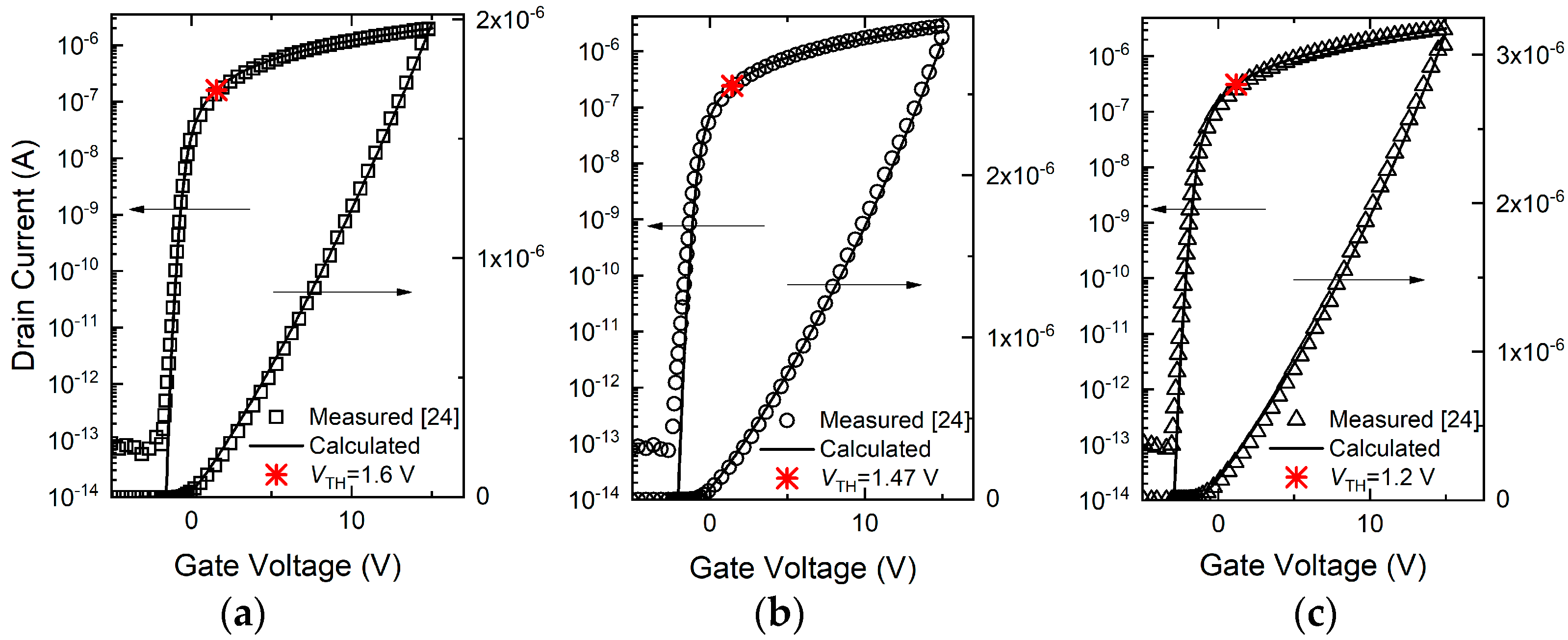
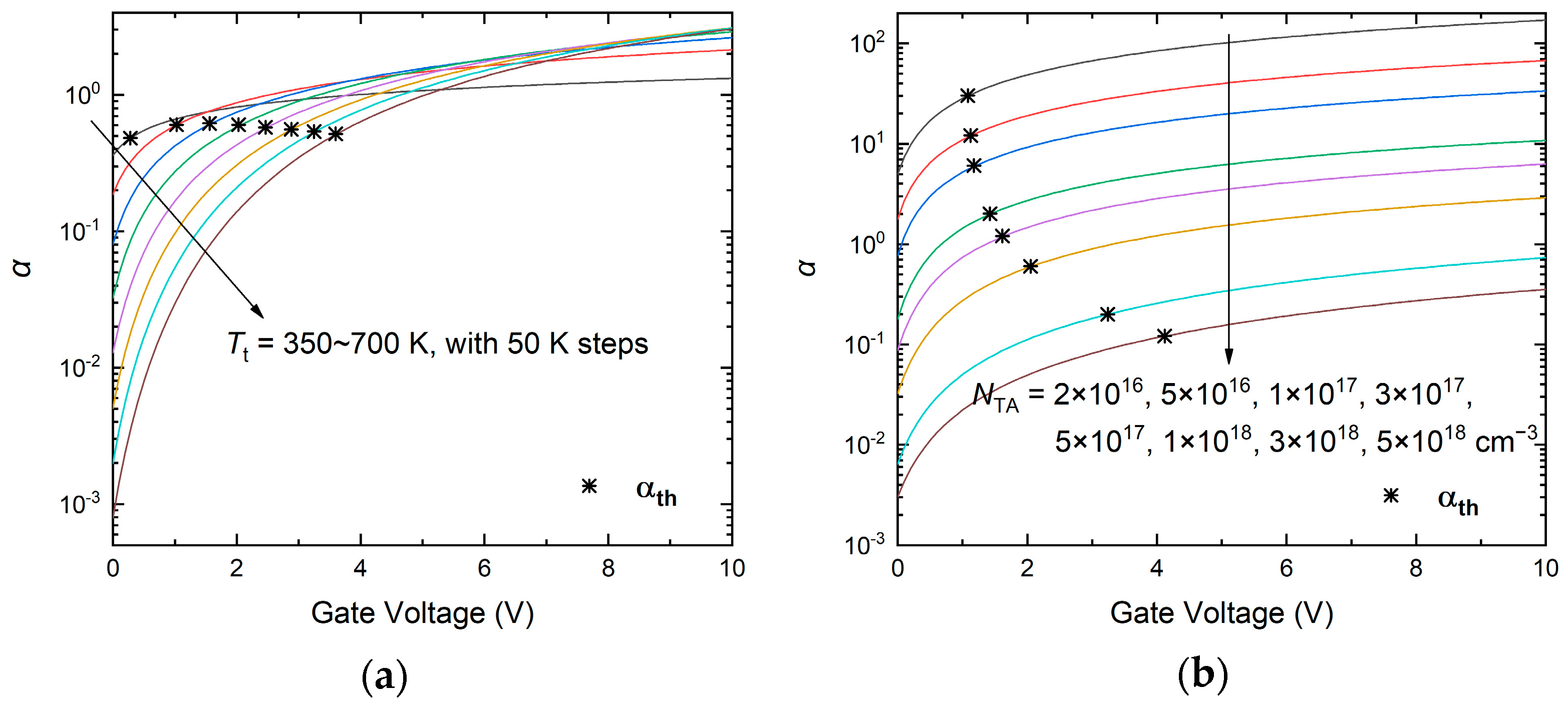
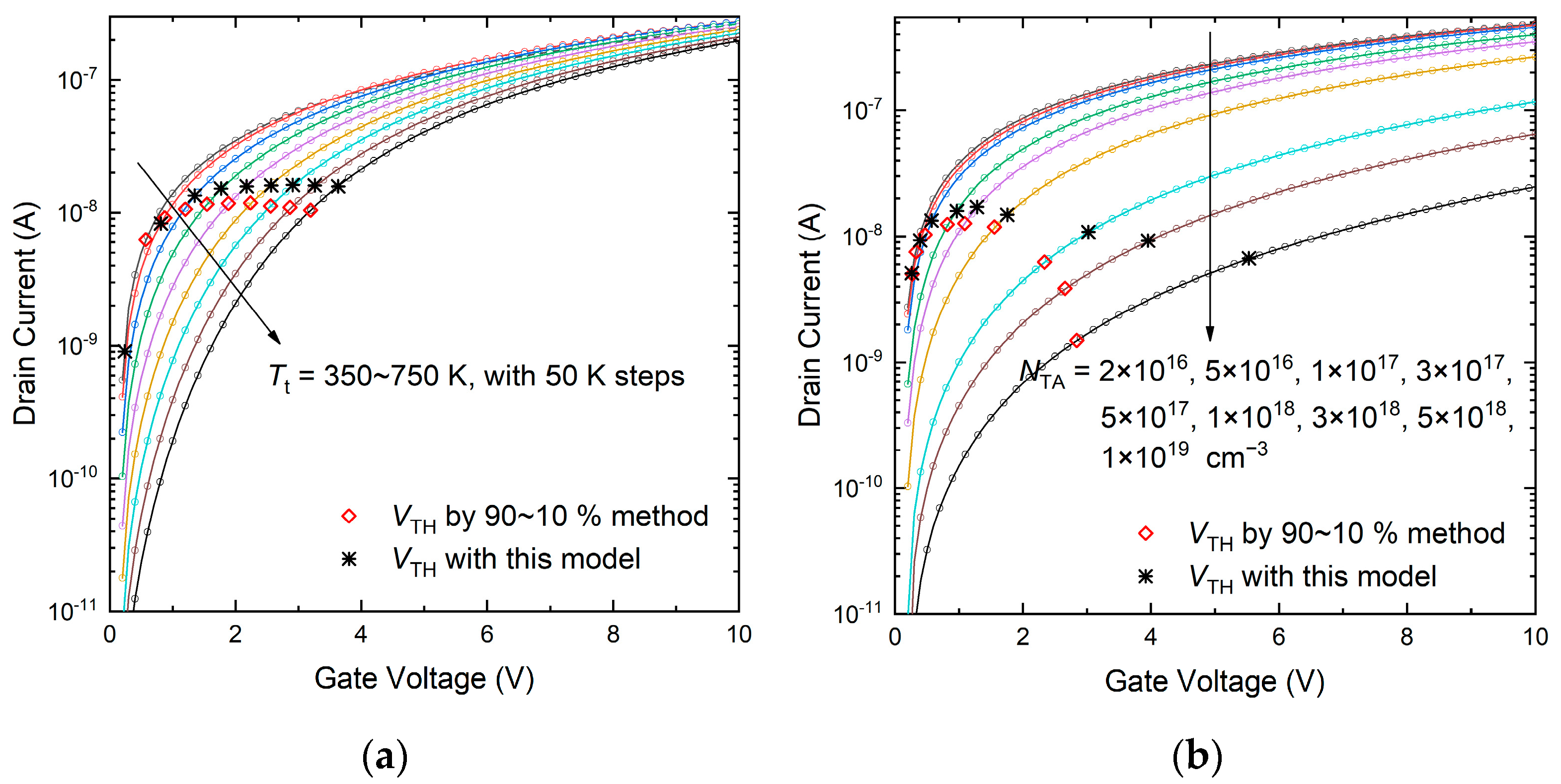
3. Results and Discussion

Figure 3a,b give the transfer characteristics (VDS = 0.1 V) of the device by Equation (18) under various Tt and NTA, with the VTH defined by Equation (12) marked on each figure. It can be observed that the transfer curves at low gate voltages (or the subthreshold slope) evidently deteriorate with the increasing Tt. On the other hand, NTA has more obvious effects on the drain current when the device is turned on. These phenomena are in accordance with the results reported in the literature [15,20]. Since kTt is the distribution slope of the band-tail states, higher kTt means the tail states exist in a wider range below the CBM. This makes the change of free charge density and thus the drain current with gate voltage less steep, especially at the subthreshold region while NTA is the total density of tail states, which contributes to the initial doping level under thermal equilibrium. Therefore, higher NTA is responsible for the lower on-current to a large extent.
Variations of VTH with NTA and Tt are displayed in Figure 4a,b, compared with those obtained by a linear extrapolation method (namely, a linear fit of the drain current between 90 to 10% of the maximum measured drain current) for AOS TFTs [23]. Parameters used in Figure 3 and Figure 4 are displayed in Table 1. Note that the NTA-axis is set as a log scale in Figure 4b to give a wider and clearer view sight of the VTH curves, and for the concerned NTA, varies in several magnitudes. It can be seen that the defined VTH shifts positively with increasing NTA and Tt, which can be explained by the conduction mechanisms in AOS TFTs. As discussed in the introduction, typically, trap-limited conduction is dominated around the threshold condition. Therefore, a higher density of tail states would trap more free carriers, resulting in a higher gate voltage for the device to turn on. It can be seen that the VTH by this model is close to those extracted by the 90~10% linear extrapolation method used in reference [23] under relatively low Tt and NTA, but begins to deviate from the latter with increasing the tail-state parameters, especially for the case of various NTA. This is because the slow-growing free charge density under high Tt or NTA results in a significant nonlinear change of drain current with gate voltage even in the linear region, making the linear extrapolation method no longer applicable.
Moreover, it should be noted that increasing VDS has little influence on the VTH by Equation (12), even in the saturation region. The theoretically calculated VTH in the saturation region is found to be very close to those from the linear region (the differences are at the magnitude of 10−4 V). The reason is that increasing VDS results in an increase in the second term and a decrease in the third term of Equation (12), which canceled each other out. However, for practical devices with very short channels, the threshold voltage extracted in the saturation region could change with VDS for short-channel effects [21]. Therefore, the threshold voltage in the linear region is more frequently used for characterizing the performance of devices [17,18]. Nevertheless, AOS TFTs show less obvious short-channel effects, which is one of the most prominent advantages compared with Si-based devices when used in electronic applications such as high-resolution displays. The short-channel effects are not included in this work at this stage (considering that it is a kind of second-order effect), which is a limitation of this work. However, the developed VTH expression could be modulated by adding a VDS-related term concerning the short-channel effects, which needs more detailed investigations on short-channel AOS TFTs in future works.
Figure 5 shows transfer curves in linear and semi-log scales calculated by Equation (20) for three different a-IGZO TFTs (lines), which give good fit to experimentally measured data (scatters) [24]. As discussed above, the distribution parameters of tail states, NTA and Tt, can be determined by fitting the calculated drain current with measured data in the subthreshold and above-threshold regions respectively. Extracted and device parameters are also displayed in Table 1. The threshold voltages calculated by Equation (12) shown in Figure 5a–c are VTH = 1.6, 1.47, 1.2 V, exhibiting appropriate values compared with those obtained by the linear extrapolation method (VTH = 1.2, 1.1, 0.8 V, respectively). It should be noted firstly that the values of VTH by linear extrapolation method are approximately obtained because of the nonlinearity of the transfer curves. Secondly, devices in Figure 5a–c have different values of flat-band voltage, which has the form of Vfb = ΔΦmsQo/Cox for practical devices [21]. Note that ΔΦms is the work-function difference between the gate metal and AOS. The Qo in the second term of Vfb includes several different types of charges: (1) interface trapped charge, (2) fixed oxide charge at (or near) the gate oxide/AOS interface, (3) mobile ionic charges in the gate oxide, (4) oxide trapped charge, (5) charges of ionized deep acceptor-like states which can be approximated as uniformly distributed in the band gap [25], as shown in Figure 1. These different types of charges are usually described by Qo located at the gate oxide/AOS interface in the device models for circuit simulation, with almost the same effect on device performance as that of the actual charge distributions. In the modeling process with measured data, the shape of transfer curves was fitted in the first place. Then, the Vfb can be easily extracted by the amounts of parallel shifts on transfer curves. Since the ΔΦms and Qo could vary for different devices, the extract Vfb can hardly be the same, which also affects the VTH. Finally, the extracted values of μe are different for devices in Figure 5a–c, as shown in Table 1, which can be explained by the different distribution of potential barriers above the CBM of different AOS layers.
Figure 5. Transfer curves (VDS = 0.5 V) calculated by Equation (20) compared with measured data of three different devices (ac) [24], with VTH by Equation (12) marked in figures.
Electronics 11 03137 g005
Table 1. Parameters in Figure 2, Figure 3, Figure 4 and Figure 5.
Parameter (Unit)Value (Figure 2, Figure 3 and Figure 4)Value (Figure 5a)Value (Figure 5b)Value (Figure 5c)
W/L (μm/μm)150/5020/2020/2020/20
Cox (nF/cm2)17.2743.143.143.1
NC (cm−3)5.2 × 10185.2 × 10185.2 × 10185.2 × 1018
T (K)300300300300
φF0 (V)0.110.110.110.11
NTA (cm−3)variable2.07 × 10171.88 × 10172.59 × 1017
Tt (K)variable120014501500
μe (cm2/Vs)1056.36.6
Vfb (V)0−1.3−1.85−2.8
β-0.0140.0180.018

4. Conclusions

A threshold voltage model for AOS TFTs has been provided in this work, which is based on the relative ratio of free-carrier density to trapped-carrier density. The developed expression for threshold voltage along with the parameter extraction procedures are analytical and directly related to distribution parameters of conduction band-tail states. Moreover, the degeneration has been included in the model derivation, thus enabling usability of this model for AOS TFTs with tail-state density varying in a wide range. Modeling results have shown that the proposed definition for threshold voltage provides physical insights into how the distribution parameters of tail states affect the threshold voltage and is suitable for practical devices.

Author Contributions

Conceptualization, M.C. and P.X.; funding acquisition, M.C., P.X. and J.C. (Jing Cao); Investigation, M.C., P.X., B.L. and Z.P.; methodology, M.C., P.X. and Z.P.; validation, M.C., B.L. and J.C. (Jing Cao); writing—original draft, M.C.; writing—review and editing, J.C. (Jianhua Cai). All authors have read and agreed to the published version of the manuscript.

Funding

This research was funded by the National Natural Science Foundation of China under Grant number 62204084, the Doctoral Research Startup Project of Hunan University of Arts and Science, grant numbers 20BSQD05 and 20BSQD06, and the Research Foundation of Education Bureau of Hunan Province, China, grant number 21B0267.

Data Availability Statement

Not applicable.

Conflicts of Interest

The authors declare no conflict of interest.

References

  1. Nomura, K.; Ohta, H.; Takagi, A.; Kamiya, T.; Hirano, M.; Hosono, H. Room-temperature fabrication of transparent flexible thin-film transistors using amorphous oxide semiconductors. Nature 2004, 432, 488–492. [Google Scholar] [CrossRef] [PubMed]
  2. Fortunato, E.; Barquinha, P.; Martins, R. Oxide semiconductor thin-film transistors: A review of recent advances. Adv. Mater. 2012, 24, 2945–2986. [Google Scholar] [CrossRef] [PubMed]
  3. Wager, J.F. TFT Technology: Advancements and opportunities for improvement. Inf. Disp. 2020, 36, 9–13. [Google Scholar] [CrossRef]
  4. Liu, P.T.; Ruan, D.B.; Yeh, X.Y.; Chiu, Y.C.; Zheng, G.T.; Sze, S.M. Highly responsive blue light sensor with amorphous Indium-Zinc-Oxide thin-film transistor based architecture. Sci. Rep. 2018, 8, 8153. [Google Scholar] [CrossRef]
  5. Cantarella, G.; Costa, J.; Meister, T.; Ishida, K.; Carta, C.; Ellinger, F.; Lugli, P.; Münzenrieder, N.; Petti, L. Review of recent trends in flexible metal oxide thin-film transistors for analog applications. Flex. Print. Electron. 2020, 5, 033001. [Google Scholar] [CrossRef]
  6. Wang, W.; Li, X.X.; Wang, T.; Huang, W.; Ji, Z.-G.; Zhang, D.W.; Lu, H.-L. Investigation of light-stimulated α-IGZO based photoelectric transistors for neuromorphic applications. IEEE Trans. Electron Devices 2020, 67, 3141–3145. [Google Scholar] [CrossRef]
  7. Chen, C.; Abe, K.; Fung, T.C.; Kumomi, H.; Kanicki, J. Amorphous In-Ga-Zn-O thin film transistor current-scaling pixel electrode circuit for active-matrix organic light-emitting displays. Jpn. J. Appl. Phys. 2009, 48, 03B025. [Google Scholar] [CrossRef]
  8. Kamiya, T.; Nomura, K.; Hosono, H. Electronic structures above mobility edges in crystalline and amorphous In-Ga-Zn-O: Percolation conduction examined by analytical model. J. Disp. Technol. 2009, 5, 462–467. [Google Scholar] [CrossRef]
  9. Lee, S.; Ghaffarzadeh, K.; Nathan, A.; Robertson, J.; Jeon, S.; Kim, C.; Song, I.-H.; Chung, U.-I. Trap-limited and percolation conduction mechanisms in amorphous oxide semiconductor thin film transistors. Appl. Phys. Lett. 2011, 98, 203508. [Google Scholar] [CrossRef]
  10. Tsormpatzoglou, A.; Hastas, N.A.; Choi, N.; Mahmoudabadi, F.; Hatalis, M.K.; Dimitriadis, C.A. Analytical surface-potential-based drain current model for amorphous InGaZnO thin film transistors. J. Appl. Phys. 2013, 114, 184502. [Google Scholar] [CrossRef]
  11. Ghittorelli, M.; Torricelli, F.; Kovács-Vajna, Z.M. Physical modeling of amorphous InGaZnO thin-film transistors: The role of degenerate conduction. IEEE Trans. Electron Devices 2016, 63, 2417–2423. [Google Scholar] [CrossRef]
  12. Fang, J.; Deng, W.; Ma, X.; Huang, J.; Wu, W. A surface-potential-based DC model of amorphous oxide semiconductor TFTs including degeneration. IEEE Electron Device Lett. 2017, 38, 183–186. [Google Scholar] [CrossRef]
  13. He, H.; Xiong, C.; Yin, J.; Wang, X.; Lin, X.; Zhang, S. Analytical drain current and capacitance model for amorphous InGaZnO TFTs considering temperature characteristics. IEEE Trans. Electron Devices 2020, 67, 3637–3644. [Google Scholar] [CrossRef]
  14. Kamiya, T.; Nomura, K.; Hosono, H. Origins of high mobility and low operation voltage of amorphous oxide TFTs: Electronic structure, electron transport, defects and doping. J. Disp. Technol. 2009, 5, 273–288. [Google Scholar] [CrossRef]
  15. Fung, T.C.; Chuang, C.S.; Chen, C.; Abe, K.; Cottle, R.; Townsend, M.; Kumomi, H.; Kanicki, J. Two-dimensional numerical simulation of radio frequency sputter amorphous In-Ga-Zn-O thin-film transistors. J. Appl. Phys. 2009, 106, 084511. [Google Scholar] [CrossRef]
  16. Kim, D.K.; Park, J.; Zhang, X.; Park, J.; Bae, J.-H. Numerical study of sub-gap density of states dependent electrical characteristics in amorphous In-Ga-Zn-O thin-film transistors. Electronics 2020, 9, 1652. [Google Scholar] [CrossRef]
  17. Qiang, L.; Yao, R. A new definition of the threshold voltage for amorphous InGaZnO thin-film transistors. IEEE Trans. Electron Devices 2014, 61, 2394–2397. [Google Scholar] [CrossRef]
  18. Chen, C.L.; Chen, W.F.; Zhou, L.; Wu, W.-J.; Xu, M.; Wang, L.; Peng, J.-B. A physics-based model of threshold voltage for amorphous oxide semiconductor thin-film transistors. AIP Adv. 2016, 6, 035025. [Google Scholar] [CrossRef]
  19. Cai, M.; Yao, R. A threshold voltage definition for modeling asymmetric dual-gate amorphous InGaZnO thin-film transistors with parameter extraction technique. J. Appl. Phys. 2019, 125, 084503. [Google Scholar] [CrossRef]
  20. Kim, Y.; Bae, M.; Kim, W.; Kong, D.; Jeong, H.K.; Kim, H.; Choi, S.; Kim, D.M.; Kim, D.H. Amorphous InGaZnO thin-film transistors-Part I: Complete extraction of density of states over the full subband-gap energy range. IEEE Trans. Electron Devices 2012, 59, 2689–2698. [Google Scholar] [CrossRef]
  21. Arora, N. MOSFET Models for VLSI Circuit Simulation: Theory and Practice; Springer: New York, NY, USA, 1993. [Google Scholar]
  22. Ghittorelli, M.; Torricelli, F.; Colalongo, L.; Kovács-Vajna, Z.M. Accurate analytical physical modeling of amorphous InGaZnO thin-film transistors accounting for trapped and free charges. IEEE Trans. Electron Devices 2014, 61, 4105–4112. [Google Scholar] [CrossRef]
  23. Fung, T.C.; Abe, K.; Kumomi, H.; Kanicki, J. Electrical instability of RF sputter amorphous In-Ga-Zn-O thin-film transistors. J. Disp. Technol. 2009, 5, 452–461. [Google Scholar] [CrossRef]
  24. Jeong, C.Y.; Park, I.J.; Cho, I.T.; Lee, J.H.; Cho, E.S.; Ryu, M.K.; Park, S.H.K.; Song, S.H.; Kwon, H.I. Investigation of the low-frequency noise behavior and its correlation with the subgap density of states and bias-induced instabilities in amorphous InGaZnO thin-film transistors with various oxygen flow rates. Jpn. J. Appl. Phys. 2012, 51, 100206. [Google Scholar] [CrossRef]
  25. Ghittorelli, M.; Kovács-Vajna, Z.M.; Torricelli, F. Physical-based analytical model of amorphous InGaZnO TFTs including deep, tail, and free states. IEEE Trans. Electron Devices 2017, 64, 4510–4517. [Google Scholar] [CrossRef]
Figure 1. Schematic band diagram of AOS with the distribution of sub-gap density of states.
Electronics 11 03137 g001
Figure 2. Variations of α with gate voltage under various (a) Tt (NTA = 1 × 1018 cm−3) and (b) NTA (T = 500 K), and αth demotes the threshold conditions, with parameters displayed in Table 1.
Electronics 11 03137 g002
Figure 3. Transfer characteristics (VDS = 0.1 V) under various tail states (a) Tt (NTA = 1 × 1018 cm−3) and (b) NTA (T = 500 K), with extracted VTH marked in the figures.
Electronics 11 03137 g003
Figure 4. Variations of threshold voltage in Figure 3 with (a) Tt (NTA = 1×1018 cm−3) and (b) NTA (T = 500 K).
Electronics 11 03137 g004
Publisher’s Note: MDPI stays neutral with regard to jurisdictional claims in published maps and institutional affiliations.

