Article

Electronically Adjustable Multiphase Sinusoidal Oscillator with High-Output Impedance at Output Current Nodes Using VDCCs

by
Koson Pitaksuttayaprot
1,
Kritphon Phanrattanachai
2,* and
Winai Jaikla
3
1
Department of Electrical Industrial Technology, Faculty of Agricultural and Industrial Technology, Phetchabun Rajabhat University, Phetchabun 67000, Thailand
2
Department of Electronics and Automation Systems Engineering, Faculty of Agricultural and Industrial Technology, Phetchabun Rajabhat University, Phetchabun 67000, Thailand
3
Department of Engineering Education, School of Industrial Education and Technology, King Mongkut’s Institute of Technology Ladkrabang, Bangkok 10520, Thailand
*
Author to whom correspondence should be addressed.
Electronics 2022, 11(19), 3227; https://doi.org/10.3390/electronics11193227
Submission received: 3 September 2022 / Revised: 25 September 2022 / Accepted: 1 October 2022 / Published: 8 October 2022
(This article belongs to the Section Circuit and Signal Processing)

Abstract

:
This paper presents the high-output-impedance current-mode multiphase sinusoidal oscillators (MSO) using voltage differencing current conveyor (VDCC)-based lossy integrators, which consist of one VDCC, one grounded capacitor, and two grounded resistors. The proposed oscillator can provide an odd-phase and even-phase system without the use of an additional amplifier. The frequency of oscillation (FO) is electronically tuned via the bias current without affecting the condition of oscillation (CO). The proposed oscillator is designed to obtain three-phase sinusoidal waveforms (n = 3). The effect of non-idealities of VDCC on the lossy integrator section is also investigated. The validity of the proposed circuit is demonstrated by PSPICE simulation using 0.18 µm TSMC CMOS process parameters with ±0.9V power supply. The frequency of oscillation obtained from the simulation is 1.43 MHz. The total harmonic distortions of the sinusoidal output currents IO1, IO2, and IO2 are 1.22%, 1.18%, and 0.57%. The IO1IO2 and IO2IO3 phase differences are approximately 121 and 119 degrees, respectively. The feasibility of the proposed MSO is also verified with experimental results using the VDCC constructed from the commercially available ICs (LT1288 and AD844) with ±5 V power supply. The results of PSPICE simulations and experiments are closely consistent with the theoretical expectation.

1. Introduction

The multiphase sinusoidal oscillator (MSO) has received a great deal of attention in many fields, such as telecommunications, where it is used for phase-shift keying (PSK) modulation [1], measurement systems, and power electronics systems [2]. Nowadays, there is a trend of synthesizing analog signal processing circuits using active building blocks (ABB) to reduce the complexity of the circuit configuration. Using an active building block requires a minimum number of passive elements. The voltage differencing current conveyor (VDCC) is significant and well-known as an active building block, being designed for the electronic circuits in analog signal processing and emphasized by electronically controllable tuning, which provides more fine-tuning than adjusting the passive-element value in both current mode (CM) and voltage mode (VM). Attracting substantial research attention, VDCC is a versatile ABB that is reported in analog signal processing publications. It is found from the literature review that many analog circuits have been realized from the VDCC. For example, PID controller [3,4], quadrature oscillator [5,6,7], universal filter [8,9,10], first-order all-pass filter [11,12], ladder filter [13], passive element simulator [14,15,16,17], and square and triangular wave generator [18,19].
Many ABBs have been employed to realize MSOs, such as operational amplifiers (OPA) [20,21], second generation current conveyors (CCII) [22,23,24], second generation current-controlled conveyors (CCCII) [25], current differencing units (CDU) [26], current amplifiers (CA) [27], operational transresistance amplifiers (OTRA) [28], dual-output voltage differencing buffered amplifiers (DO-VDBA) [29], current-feedback amplifiers (CFA) [30], current differencing transconductance amplifiers (CDTA) [31,32], current differencing buffered amplifiers (CDBA) [33], voltage differencing differential difference amplifiers (VDDDA) [34], current-controlled current differencing transconductance amplifiers (CCCDTA) [35] and current-feedback operational amplifiers (CFOA) [36]. The MSO proposed in [31] requires two CDTAs per phase. In [22,28,30,31,32,33], the frequency of oscillation (FO) and the condition of oscillation (CO) are not independently controlled. The FO of the MSOs proposed in [20,21,22,23,24,26,28,30,32,33,36] is not electronically adjustable on the FO. The capacitors in [28,29,31,32] are not grounded capacitors. Requiring additional amplifiers [20,21,23,26,28,31,33] complicates circuits. A comparison table for the proposed MSO with other MSOs [20,21,22,23,24,25,26,27,28,29,30,31,32,33,34,35,36] is given in Table 1.
In this paper, the VDCC-based multiphase sinusoidal oscillator is proposed. The gain-controllable lossy integrators are used to realize the proposed multiphase sinusoidal oscillators. The lossy integrator consists of one VDCC, one grounded capacitor, and two grounded resistors. Using only one VDCC and grounded passive elements per phase is ideal for integration. The FO and the CO are independently controlled. Additionally, the frequency of oscillation is electronically tuned. Finally, the PSPICE simulation and experimental results are given to verify the performance of the proposed MSO.

2. Principle of Operation

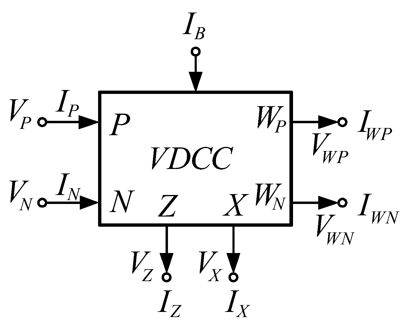
2.1. Basic Concept of VDCC

A voltage differencing current conveyor (VDCC) is a six-terminal active building block. The P and N voltage input terminals have high impedance, the Z current output terminal has high impedance, the X current input and voltage output terminal have low impedance, and the WP and WN current output terminals have high impedance. The magnitude of current at WP and WN terminals is the same, but they are in opposite directions. The VDCC is an active device operating both current and voltage mode systems. The electrical symbols and equivalent circuits of the VDCC are shown in Figure 1 and Figure 2, respectively. Using the hybrid matrix form, we can describe the electrical properties of VDCC as follows [37]:
[ I N I P I Z V X I W P I W N ] = [ 0 0 0 0 0 0 0 0 g m g m 0 0 0 0 1 0 0 0 0 1 0 0 0 1 ] [ V P V N V Z I X ] ,
where gm denotes the transconductance gain, which is controlled by the DC bias current IB for CMOS VDCC as follows [37]:
g m = I B μ n C O X W / L ,
where IB is bias current, μn is the mobility of the carrier for MOS transistors, COX is the gate-oxide capacitance per unit area, W is effective channel width, and L is effective channel length, respectively. The internal construction of the CMOS VDCC employed for the realization of the proposed MSO is presented in [37].

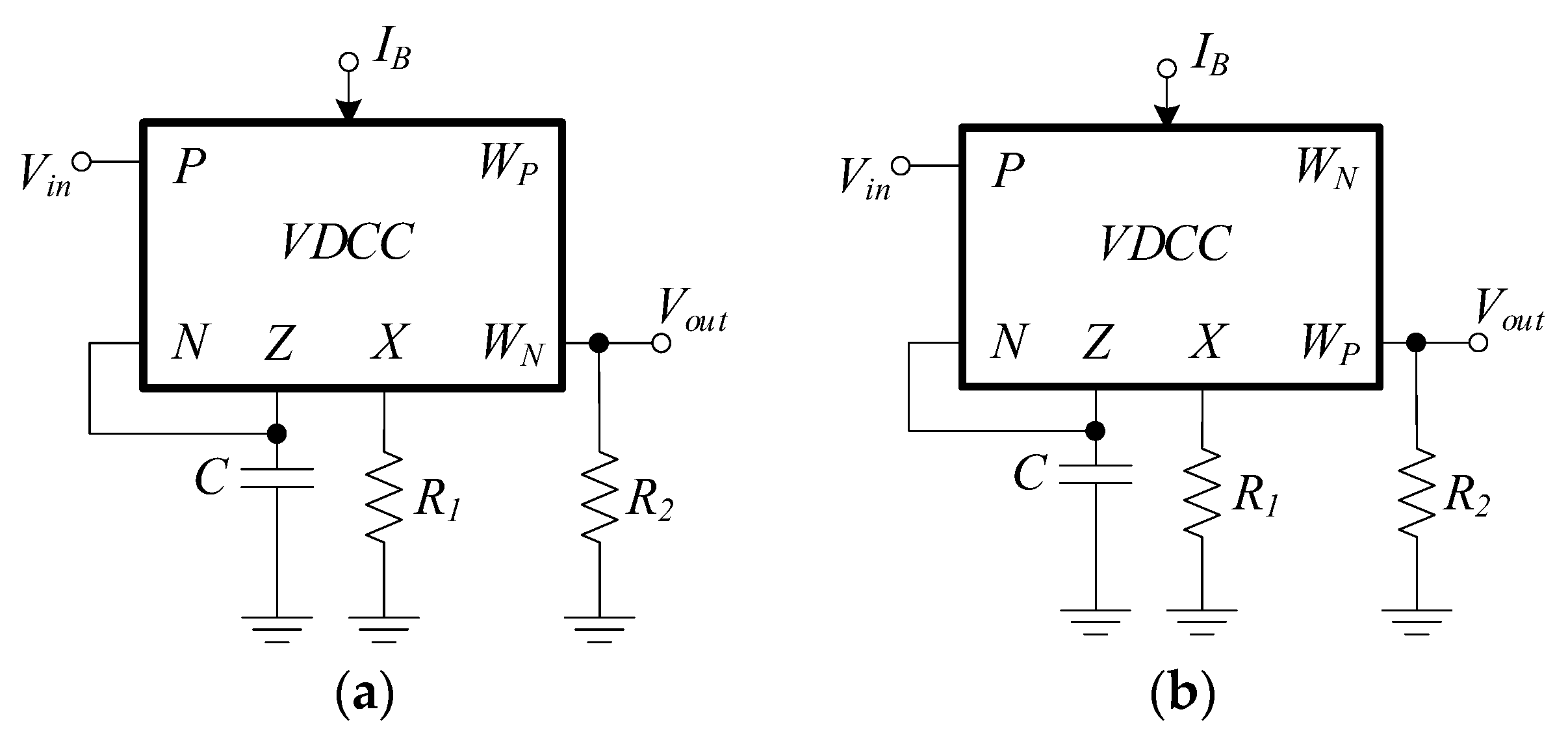
2.2. Design of MSOs Using Lossy Integrator Circuit

The generalized structures of MSOs are realized from the principle proposed in [23,24,36], which contains the lossy integrator (first-order low-pass filter: LPF) for each phase by cascading the n identical stages (n ≥ 3). The input of the first stage is provided by the feedback output from the nth stage, and the last section is inverted for odd-phase systems and non-inverted for even-phase systems. Each system, without any additional external amplifier, can give one phase per one lossy integrator. The system loop gain for the odd-phase system can be written as follows:
L ( s ) = ( k s a + 1 ) n ,
and the system loop gain for the even-phase system is given by:
L ( s ) = ( 1 ) n 1 ( k s a + 1 ) n ,
where the variable k is the voltage gain, and the variable α denotes the time constant of each integrator section. The system loop gain for the odd-phase system and even-phase system is given by:
L ( s ) = ( k s a + 1 ) n = 1 ,
At oscillation frequency (s = osc), the system loop gain is given by:
( j ω o s c a + 1 ) n + ( k ) n = 0 ,
The Barkhausen’s condition of the magnitude and phase of the system loop gain are given as:
| L ( j ω o s c ) | = 1 ,
and
L ( j ω o s c ) = n ϕ = π n tan 1 ( ω o s c a ) = 2 π ,
where ϕ is the phase shift of each lossy integrator. Considering Equations (7) and (8), the frequency of oscillation (FO) and the condition of oscillation (CO) are expressed as [34,35,36]:
FO :   ω o s c = 1 a tan ( π n ) ,
and
CO :   k sec ( π n ) ,
Considering Equations (9) and (10), the FO can be controlled independently of the CO by the time constant α, while the CO can be changed by the gain k without affecting the FO.

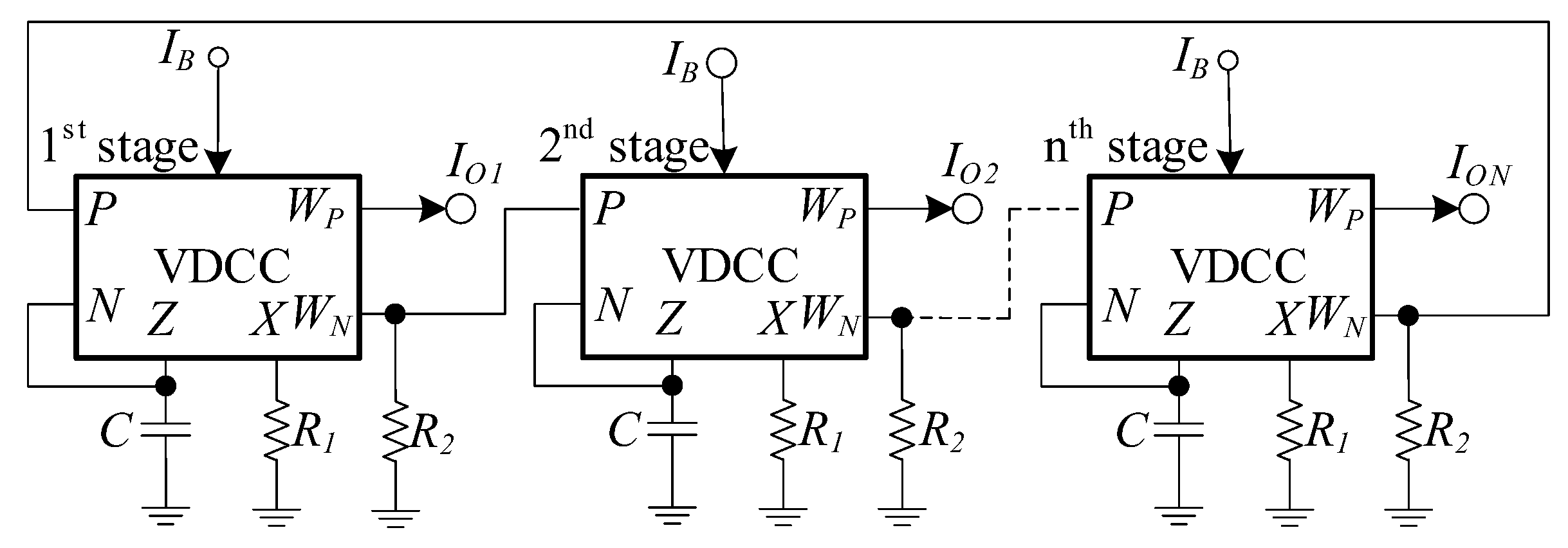
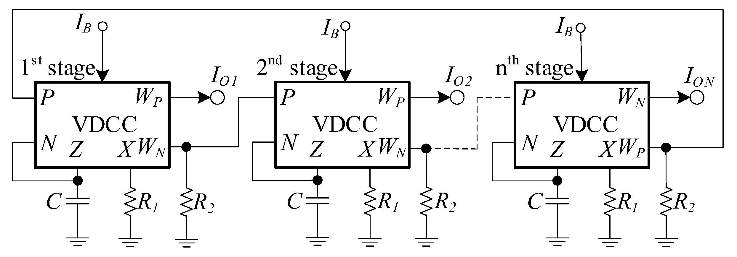
2.3. Implementation of n-Cascaded Lossy Integrator-Based Multiphase Sinusoidal Oscillator

The proposed MSO is based on lossy integrator sections, as mentioned in the preceding section. Figure 3 depicts a potential VDCC-based inverting and non-inverting lossy integrator implementation where the output voltage nodes of the inverting and non-inverting integrators are at nodes WN and WP, respectively. The input voltage node is high impedance. The proposed lossy integrators consist of 1 VDCC, 1 grounded capacitor, and 2 grounded resistors. The voltage transfer function of the lossy integrator is given by:
T ( s ) = V o u t V i n = ± R 2 R 1 s C g m + 1 ,
Based on Equation (3), the k = R2/R1 and α = C/gm. According to Equations (9) and (10), the FO and the CO are as follows:
FO :   ω o s c = g m C tan ( π n ) ,
and
CO :   R 2 R 1 sec ( π n ) .
Considering Equations (12) and (13), the FO can be electronically and independently tuned from the CO by the bias current IB, while the CO can be controlled by the resistors R1 and R2 without affecting the FO. For amplitude stabilization, each gain-controllable lossy integrator uses a resistor R1 that is readily constructed from a photoresistor to stabilize the output amplitude level. The 3WK16341 optocoupler with photoresistor [38] contains this component. Additional information on amplitude stabilization using 3WK16341 is provided in [39,40].
Using the identical inverting lossy integrator in Figure 3a yields the proposed odd-phase MSO shown in Figure 4. For connecting the output terminals to the load or other circuits without using an additional buffer, the output is the current (IO) flowing out from the WN terminal. Using the inverting lossy and non-inverting integrators in Figure 3a,b yields the proposed even-phase MSO as shown in Figure 5. Using all grounded passive elements is ideal for integration. Moreover, two grounded resistors R1 and R2 can be implemented from two MOS transistors [41] which will be voltage-controllable.

2.4. Non-Ideal Analysis

The effect of two non-ideal VDCC properties on the performances of the proposed MSO is studied in this section. These non-ideal cases include parasitic elements and voltage/current tracking errors. The parasitic elements of the parallel-RC impedance appearing at the high impedance input and output terminals are as follows: RP, CP, RN, and CN are at the voltage input P and N terminals, respectively; RZ and CZ are at the current output Z terminal; and RWP, CWP, RWN, and CWN are at the current output WP and WN terminals, respectively. The RX appears in series at the low-impedance X terminal. The β parameter is the voltage tracking error from the Z terminal to the X terminal, and the α parameter is the current tracking error from the X terminal to the WP and WN terminal. The model of the proposed non-ideal lossy integrator circuit with parasitic elements is shown in Figure 6.
The two-pole model [30,36] is employed to investigate the effect of the proposed non-ideal lossy integrator, which can be written in the normal form of the two-pole model as:
V o u t ( s ) V i n ( s ) = K ( s ω a + 1 ) ( s ω p 2 + 1 ) ,
where K is the voltage gain, ωa is the dominant pole, and ωp2 is the second pole. Based on the circuit in Figure 6, the transfer function of the non-ideal lossy integrator can be expressed as:
V o u t ( s ) V i n ( s ) = α β g m R a * R p 2 * R 1 * ( R a * C a * s + 1 ) ( R p 2 * C p 2 * s + 1 ) ,
where R a * = R N R Z 1 g m , C a * = C N + C Z + C , R p 2 * = R P R W N R 2 , C p 2 * = C P + C W N and R 1 * = R X + R 1 . Based on Equation (14), the voltage gain, the dominate pole, and the second pole can be expressed as:
K = [ α β ( R P R W N R 2 ) R X + R 1 ] [ ( R N R Z 1 g m ) g m ] ,
ω a = 1 ( R N R Z 1 g m ) ( C N + C Z + C ) ,
and
ω p 2 = 1 ( R P R W N R 2 ) ( C P + C W N ) .
From Equation (18), the transfer function of the non-ideal lossy integrator provides an additional pole called the second pole, which is derived from the parasitic parameters. This pole mainly causes the limitation at high frequencies. According to CMOS VDCC construction, the parasitic parameters are as follows: RP = 4.38 TΩ, CP = 0.034 pF, RN = 4.3875 TΩ, CN = 0.0344 pF, RZ = 229.426 kΩ, CZ = 0.025 pF, RWP = 186.658 kΩ, CWP = 0.0105 pF, RWN = 175.278 kΩ, CWN = 0.022 pF. At R2 = 2 kΩ, the frequency of the second pole is approximately 1.44 GHz. From Equation (18), R2 should be set to a low value to enhance the second pole’s frequency. If the ωp2 is much higher than ωa (ωp2 >> ωa), the second pole has a slight effect on the performance of the proposed MSO system. Therefore, the Barkhausen criterion yields the FO and the CO as:
ω o s c = 1 ( R N R Z 1 g m ) ( C N + C Z + C ) tan ( π n ) ,
and
α β g m ( R N R Z 1 g m ) ( R P R W N R 2 R X + R 1 ) sec ( π n ) .
It is found from Equation (19) that the affected dominant pole by the RN, RZ, CN, and CZ parasitic parameters reduces the performance of the FO. The CO is also affected by voltage/current tracking errors and parasitic elements, as shown in Equation (20). Moreover, it is found that the transconductance, gm, will slightly affect the CO due to the parasitic resistance RN and RZ. The parasitic resistance RZ can be varied by adjusting IB.

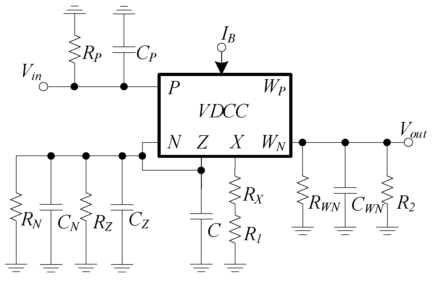
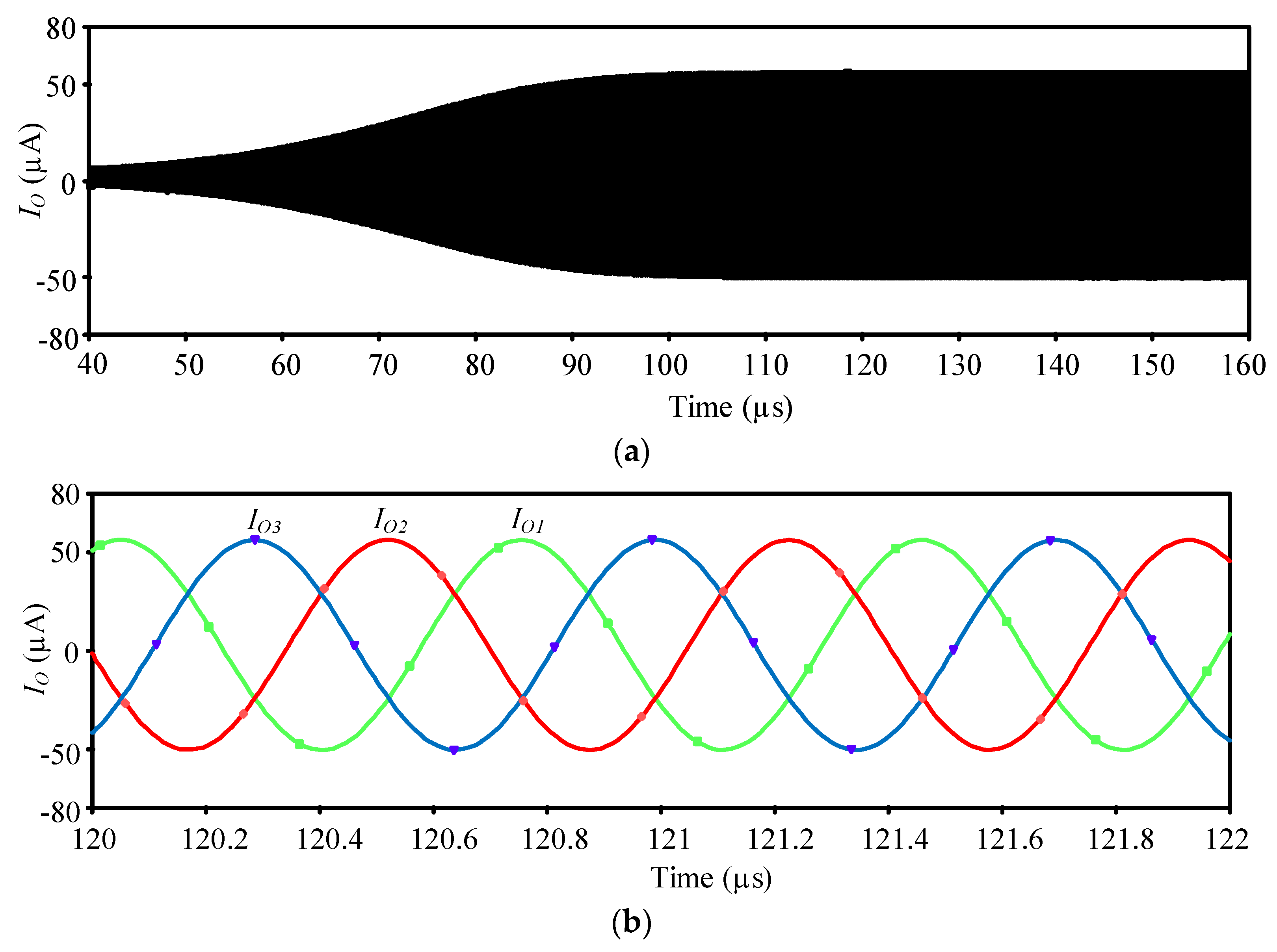
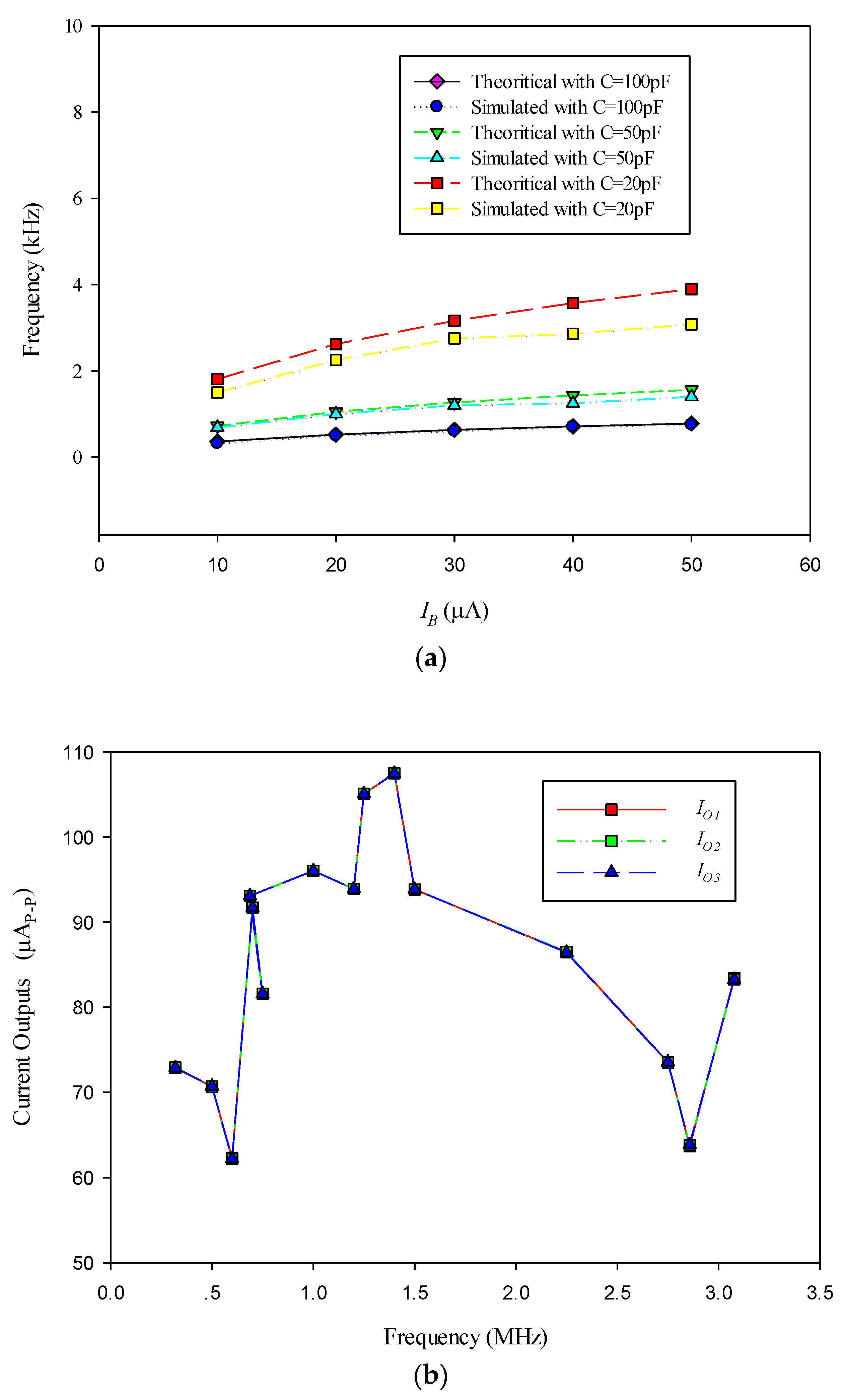
3. Simulation Results

A PSPICE simulation simulated the proposed multiphase sinusoidal oscillator’s performance with TSMC 0.18 µm CMOS process parameters [7,37]. The simulation was performed using the CMOS VDCC structure proposed in [37] with ±0.9 V power supply. The MOS aspect ratios are given in Table 2 [37]. Based on the circuit in Figure 4, the three-phase sinusoidal oscillator was designed. The three-phase sinusoidal oscillator was used to directly produce the generator magnetomotive forces [42]. The bias currents were set as IB = 50 µA (gm = 282 µA/V) and IB0 = 100 µA. The values of the passive elements were set as R1 = 1 kΩ, R2 = 2.05 kΩ, and C = 50 pF. The theoretical FO calculated from Equation (12) was 1.55 MHz. Figure 7a depicts the simulated transient current-output waveform, and Figure 7b shows the steady-state current-output waveform where the simulated FO is 1.43 MHz with a 7.74% error. Figure 7c shows the simulated output spectrum, with the IO1 having a THD of approximately 1.22%, the IO2 having a total THD of about 1.18%, and the IO3 having a THD of about 0.57%. The phase difference between IO1 and IO2 was about 121 degrees, and the phase difference between IO2 and IO3 was about 119 degrees.
As illustrated in Figure 8a, varying the biased current (IB) with different capacitance values yields good results of FO from the proposed MSO circuit. Figure 8b shows the magnitude of the current output waveforms during frequency tuning. The phase difference between current outputs (IO1 and IO2) and the phase difference between current outputs (IO2 and IO3) are depicted in Figure 8c. By adjusting the FO, the THD values in Figure 8d varied from 0.57% to 7.09%. The power consumption of the proposed circuit obtained from the simulation was approximately 2.36 mW.

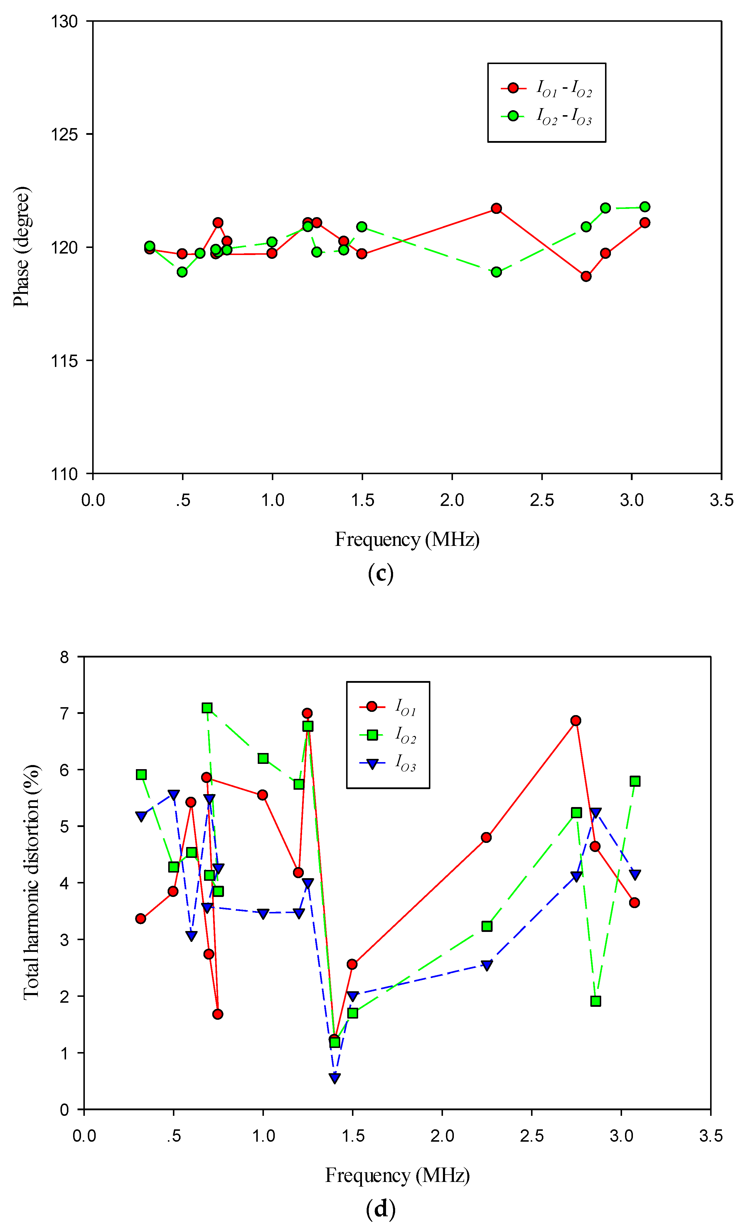
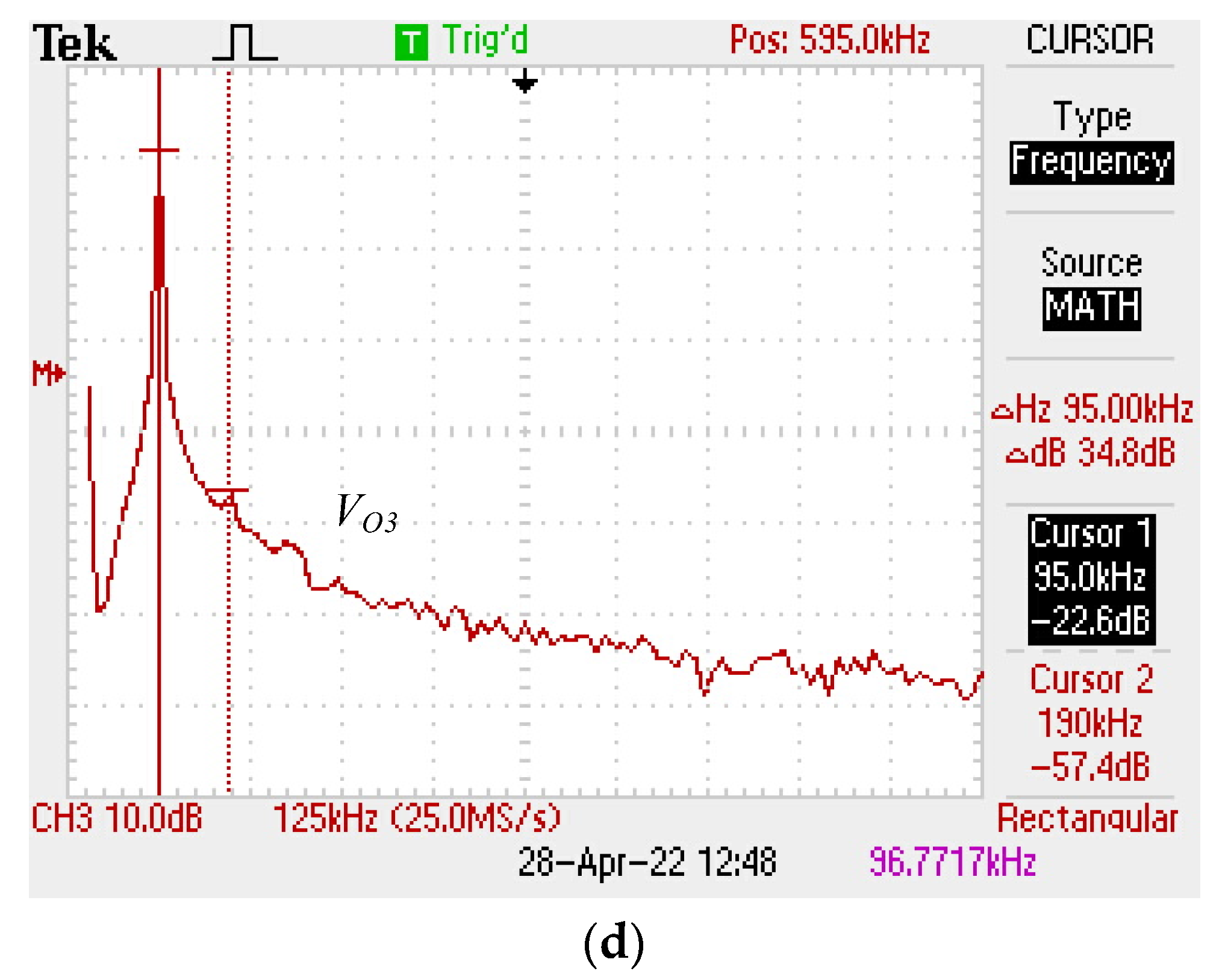
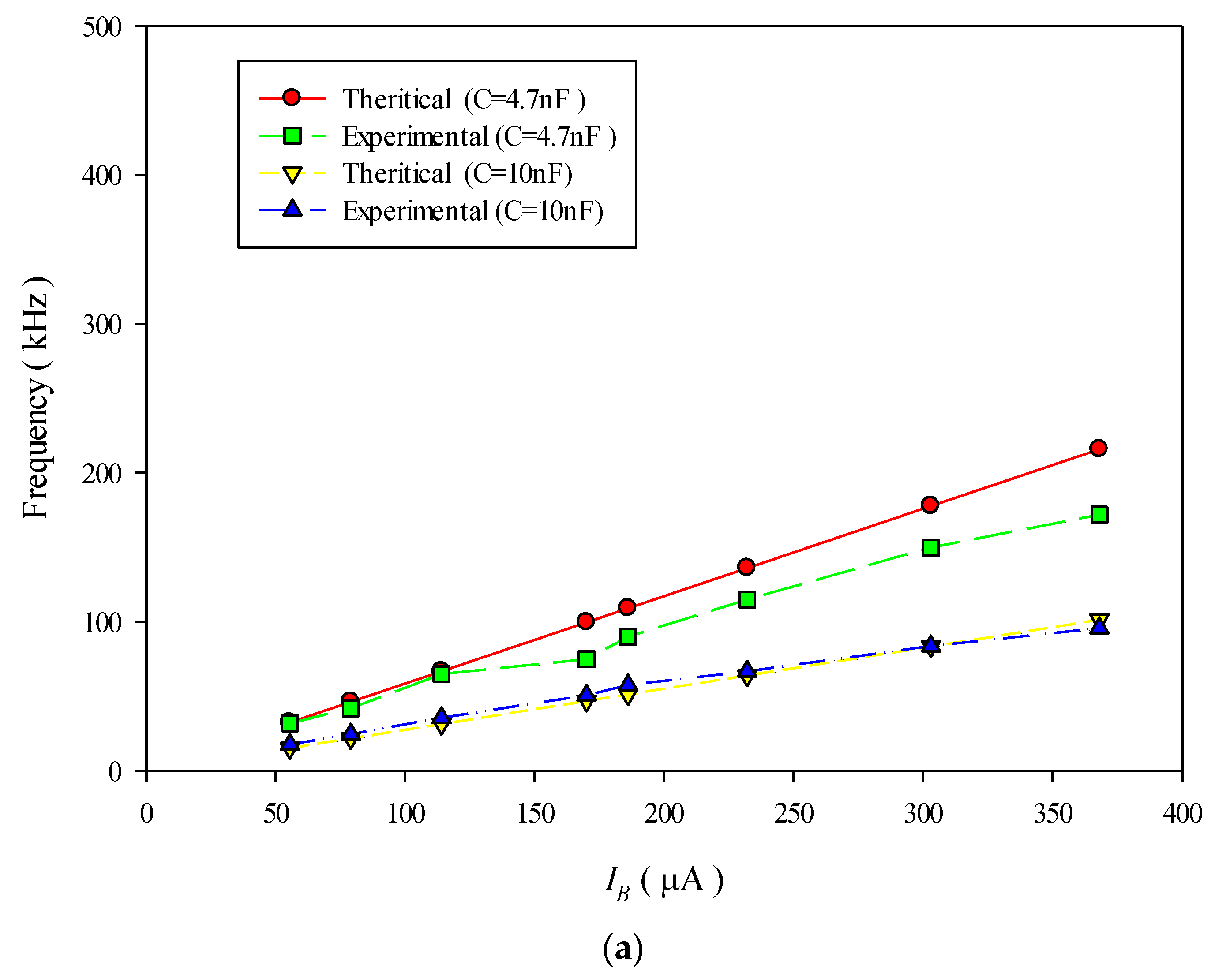
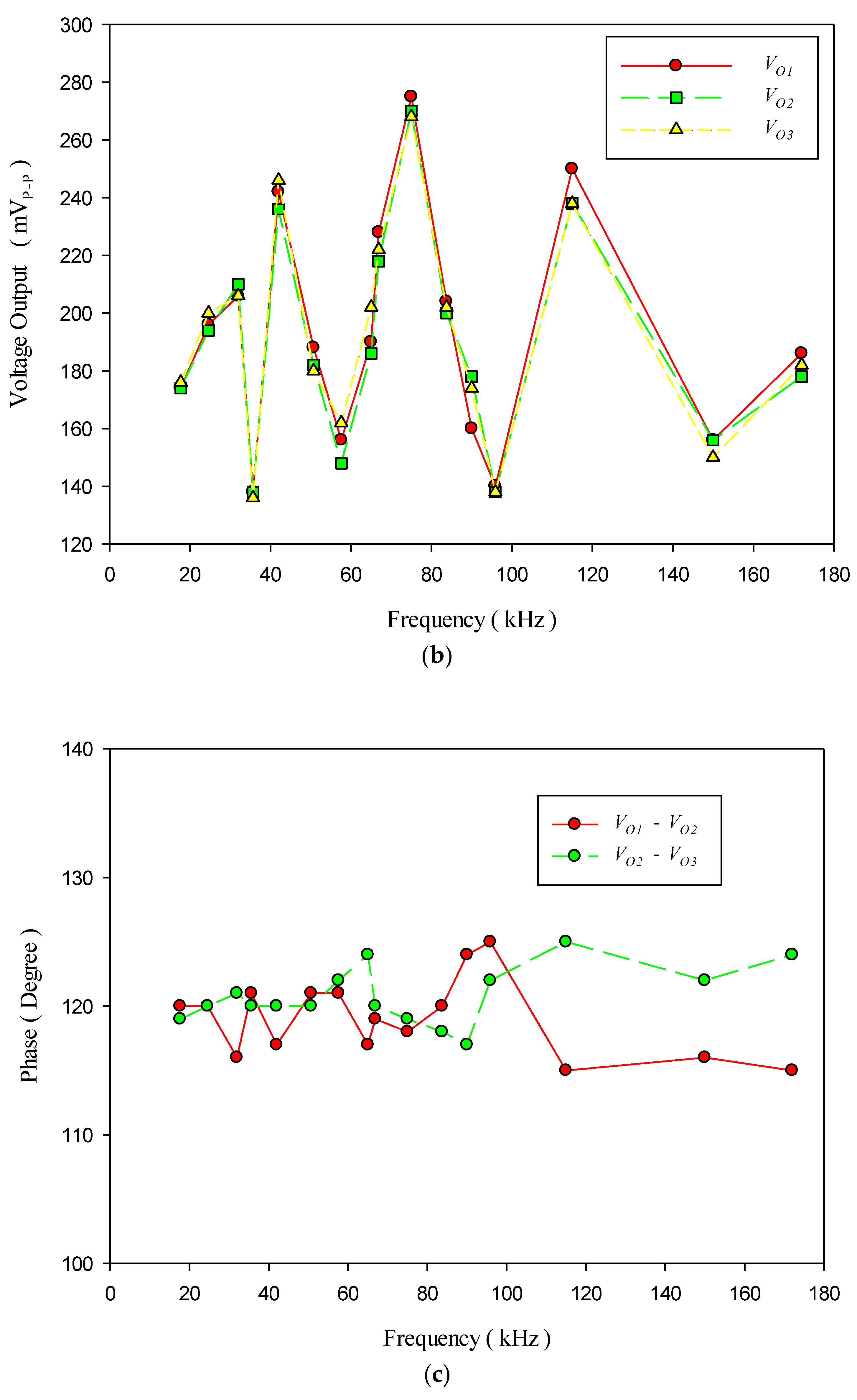
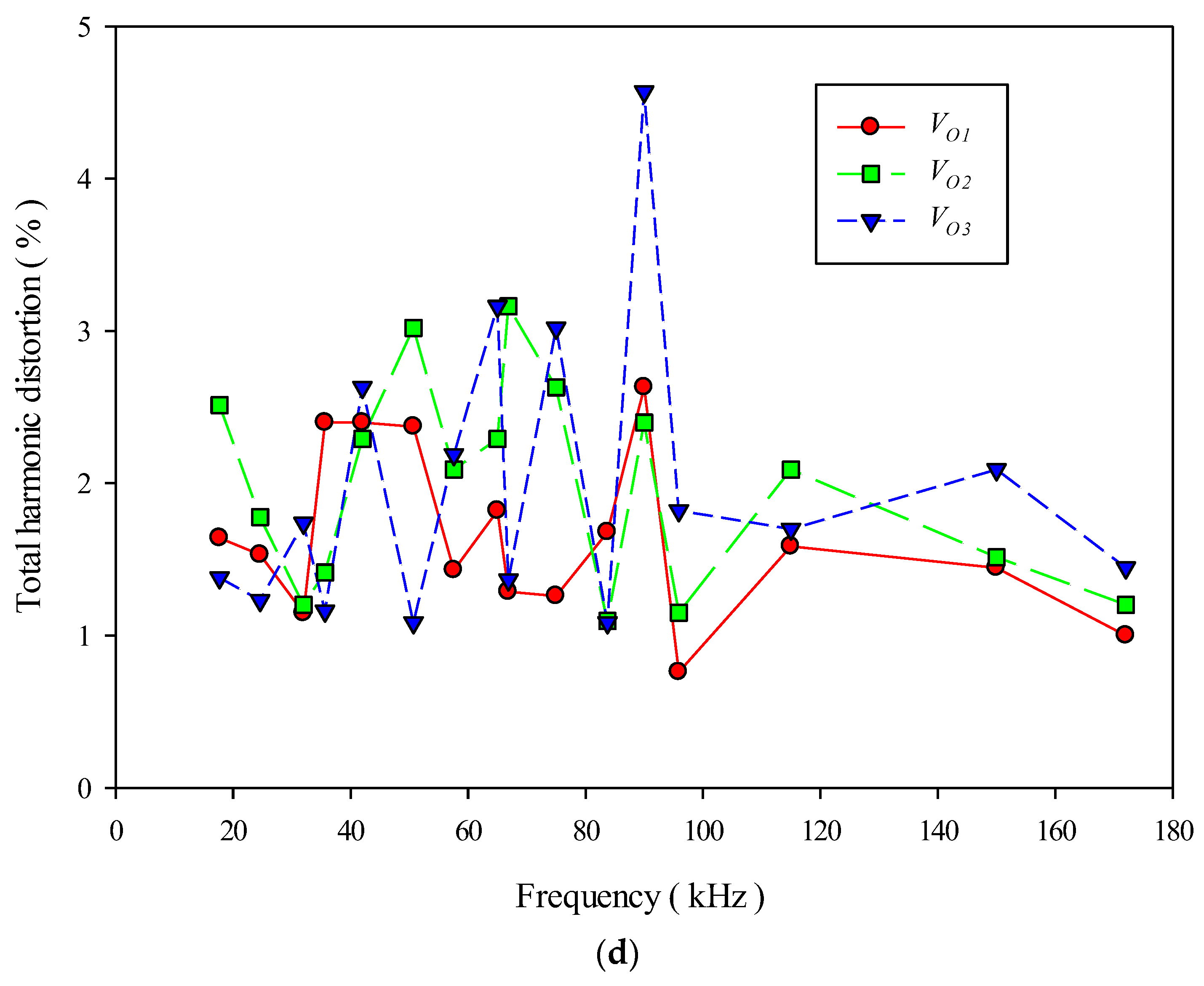
4. Experimental Results

For the experiment, the inverting and non-inverting lossy integrators were built up, as shown in Figure 9. The VDCC was constructed from the commercially available ICs LT1228 and AD844. For inverting the lossy integrator in Figure 9a, the resistor R1 was connected in a floating configuration between the output of the voltage buffer in LT1228 and the X terminal of AD844. Nevertheless, all passive elements were grounded in the non-inverting lossy shown in Figure 9b. This VDCC structure contains only one W terminal. Therefore, when the lossy integrator is constructed as the multiphase oscillator, the output waveforms for the experiment are the voltage dropped on the resistor R2. The gm for this construction is given as:
g m = 10 I B .
To validate the functionality of the proposed MSO, a three-phase system (n = 3) was designed using the inverting lossy integrator in Figure 9a with ±5 V power supply. The value of the bias current was set as IB = 368 µA (gm is 3.68 mA/V). The passive elements were chosen as R1 = 1 kΩ, R2 = 2.2 kΩ, and C = 10 nF. The theoretical FO calculated from Equation (12) was 101 kHz. Figure 10a shows the voltage output waveform where the experimental FO is about 95 kHz. Figure 10b, 10c and 10d show the experimental output spectrum, with the VO1 having a THD of approximately 0.76%, the VO2 having a total THD of about 1.15%, and the VO3 having a THD of about 1.82%.
Figure 11a shows the results of the FO by adjusting IB with different capacitance values. The magnitudes of the voltage output waveforms in Figure 11b range from 136 mVP-P to 275 mVP-P, which are similar to their magnitudes at the same frequency. As a result of maintaining the linear region operation of the operational transconductance amplifiers (OTAs), when the FO or IB increases, all of the magnitudes tended to decrease. The phase differences of voltage outputs in Figure 11c are close to 120°. The THD values of the voltage outputs varied from 0.76% to 4.57%, as shown in Figure 11d. The power consumption of the proposed circuit obtained from the experiment was approximately 0.38 W.

5. Conclusions

The proposed multiphase sinusoidal oscillator based on a lossy integrator structure has been presented. As it is composed of n-cascaded lossy integrators, the proposed oscillators provide even-phase or odd-phase sinusoidal waveforms without using an additional amplifier. The oscillation frequency is electronically tuned without affecting the oscillation condition. The proposed concept has been evaluated using PSPICE simulations with TSMC 0.18 µm CMOS process parameters. The simulated FO is 1.43 MHz with a 7.74% error. The THDs for IO1, IO2, and IO2 are 1.22%, 1.18%, and 0.57%, respectively. The phase difference between IO1 and IO2 is about 121 degrees, and the phase difference between IO2 and IO3 is about 119 degrees. The power consumption of the proposed circuit obtained from the simulation is approximately 2.36 mW. Additionally, the hardware implementation based on the commercial ICs LT1228 and AD844 was tested. All fundamental mathematical analyses have been included, such as ideal, non-ideal, and parasitic parameters.

Author Contributions

Conceptualization, K.P. (Koson Pitaksuttayaprot) and W.J.; methodology, K.P. (Koson Pitaksuttayaprot) and W.J.; validation, K.P. (Koson Pitaksuttayaprot), W.J. and K.P. (Kritphon Phanrattanachai); formal analysis, K.P. (Koson Pitaksuttayaprot) and W.J.; investigation, K.P. (Koson Pitaksuttayaprot) and W.J.; writing—original draft preparation, K.P. (Koson Pitaksuttayaprot), W.J. and K.P. (Kritphon Phanrattanachai); writing—review and editing, K.P. (Koson Pitaksuttayaprot), W.J. and K.P. (Kritphon Phanrattanachai). All authors have read and agreed to the published version of the manuscript.

Funding

This research received no external funding.

Acknowledgments

The experiments were carried out in the Analog Circuits Design Lab of the Electronics Technology Department, Faculty of Agricultural and Industrial Technology, Phetchabun Rajabhat University, Thailand.

Conflicts of Interest

The authors declare no conflict of interest.

References

  1. Fouda, M.E.; Soltan, A.; Radwan, A.G.; Soliman, A.M. Fractional-order multi-phase oscillators design and analysis suitable for higher-order PSK applications. Analog Integr. Circuits Signal Process. 2016, 87, 301–312. [Google Scholar] [CrossRef]
  2. Jang, Y.; Jovanovic, M.M.; Panov, Y. Multiphase buck converters with extended duty cycle. In Proceedings of the Twenty-First Annual IEEE Applied Power Electronics Conference and Exposition (APEC’06), Dallas, TX, USA, 19–23 March 2006; pp. 38–44. [Google Scholar]
  3. Domansky, O.; Sotner, R.; Langhammer, L.; Jerabek, J.; Psychalinos, C.; Tsirimokou, G. Practical design of RC approximants of constant phase elements and their implementation in fractional-order PID regulators using CMOS voltage differencing current conveyors. Circuits Syst. Signal Process. 2019, 38, 1520–1546. [Google Scholar] [CrossRef]
  4. Özer, E.; Kaçar, F. Design of voltage-mode PID controller using a single voltage differencing current conveyor (VDCC). Analog Integr. Circuits Signal Process. 2021, 109, 11–27. [Google Scholar] [CrossRef]
  5. Prasad, D.; Ahmad, J.; Srivastava, M. New CM/VM 3rd-order quadrature oscillator using VDCCs. In Proceedings of the International Conference on Applied System Innovation (ICASI), Sapporo, Japan, 13–17 May 2017; pp. 1328–1330. [Google Scholar]
  6. Roy, S.; Pal, R.R. Electronically tunable third-order dual-mode quadrature sinusoidal oscillators employing VDCCs and all grounded components. Integration 2021, 76, 99–112. [Google Scholar] [CrossRef]
  7. Srivastava, M.; Prasad, D. VDCC based dual-mode quadrature sinusoidal oscillator with outputs at appropriate impedance levels. Adv. Electr. Electron. Eng. 2016, 14, 168–177. [Google Scholar] [CrossRef]
  8. Arora, T.S. Realization of current-mode universal filter utilising minimum active elements and only grounded passive components. In Proceedings of the 2020 7th International Conference on Signal Processing and Integrated Networks (SPIN), Noida, India, 27–28 February 2020; pp. 681–686. [Google Scholar]
  9. Lamun, P.; Phatsornsiri, P.; Torteanchai, U. Single VDCC-based current-mode universal biquadratic filter. In Proceedings of the 2015 7th International Conference on Information Technology and Electrical Engineering (ICITEE), Chiang Mai, Thailand, 29–30 October 2015; pp. 122–125. [Google Scholar]
  10. Rana, S.; Kumawat, A.K.; Kumar, P. A universal current mode KHN biquad filter using voltage differencing current conveyor. In Proceedings of the 2016 IEEE 1st International Conference on Power Electronics, Intelligent Control and Energy Systems (ICPEICES), Delhi, India, 4–6 July 2016; pp. 1–5. [Google Scholar]
  11. Cheta, W.; Siripruchyanun, M.; Trachu, K.; Suwanjan, P.; Sotner, R.; Jaikla, W. Single VDCC based voltage-mode first-order allpass filter with electronic controllability. In Proceedings of the 2018 18th International Symposium on Communications and Information Technologies (ISCIT), Bangkok, Thailand, 26–29 September 2018; pp. 255–260. [Google Scholar]
  12. Uttaphut, P. Voltage-Mode first-order allpass filter with grounded capacitor and electronic controllability. Przegląd Elektrotechniczny 2019, 95, 101–104. [Google Scholar] [CrossRef]
  13. Prasad, D.; Ahmad, A.; Shukla, A.; Mukhopadhyay, A.; Sharma, B.B.; Srivastava, M. Novel VDCC based low-pass and high-pass ladder filters. In Proceedings of the 2015 Annual IEEE India Conference (INDICON), New Delhi, India, 17–20 December 2015; pp. 1–3. [Google Scholar]
  14. Kartci, A.; Ayten, U.E.; Herencsar, N.; Sotner, R.; Jerabek, J.; Vrba, K. Floating capacitance multiplier simulator for grounded RC colpitts oscillator design. In Proceedings of the 2015 International Conference on Applied Electronics (AE), Pilsen, Czech Republic, 8–9 September 2015; pp. 93–96. [Google Scholar]
  15. Kumar, R.; Kumar, A.; Bhardwaj, K.; Srivastava, M. Active realization of series inductor and shunt capacitor and their applications in electronically tunable wave active filters. In Proceedings of the 2021 5th International Conference on Computing Methodologies and Communication (ICCMC), Erode, India, 8–10 April 2021; pp. 683–688. [Google Scholar]
  16. Srivastava, M.; Roy, A.; Singh, R.; Gupta, P. New VDCC based electronically tunable grounded frequency dependent negative resistance simulator employing grounded passive elements. In Proceedings of the 2017 Recent Developments in Control, Automation & Power Engineering (RDCAPE), Noida, India, 26–27 October 2017; pp. 313–317. [Google Scholar]
  17. Kumar, K.N.; Mouli, P.C.; Das, K.S.; Srivastava, M. Novel Electronic/Resistance Adjustable Capacitance Multiplier Circuit with VDCCs and Grounded Resistances. In Proceedings of the 2019 6th International Conference on Signal Processing and Integrated Networks (SPIN), Noida, India, 7–8 March 2019; pp. 1112–1115. [Google Scholar]
  18. Jerabek, J.; Sotner, R.; Dostal, T.; Vrba, K. Simple resistor-less generator utilizing z-copy controlled gain voltage differencing current conveyor for PWM generation. Elektron. Ir Elektrotechnika 2015, 21, 28–34. [Google Scholar] [CrossRef] [Green Version]
  19. Sotner, R.; Jerabek, J.; Herencsar, N.; Dostal, T.; Vrba, K. Design of Z-copy controlled-gain voltage differencing current conveyor based adjustable functional generator. Microelectron. J. 2015, 46, 143–152. [Google Scholar] [CrossRef]
  20. Gift, S.J. Multiphase sinusoidal oscillator system using operational amplifiers. Int. J. Electron. 1997, 83, 61–68. [Google Scholar] [CrossRef]
  21. Gift, S.J.G. The application of all-pass filters in the design of multiphase sinusoidal systems. Microelectron. J. 2000, 31, 9–13. [Google Scholar] [CrossRef]
  22. Minhaj, N. Second-generation current conveyor-based even/odd multiphase sinusoidal oscillators. In Proceedings of the 2009 International Conference on Advances in Recent Technologies in Communication and Computing, Kottayam, India, 27–28 October 2009; pp. 231–235. [Google Scholar]
  23. Hou, C.L.; Shen, B. Second-generation current conveyor-based multiphase sinusoidal oscillators. Int. J. Electron. 1995, 78, 317–325. [Google Scholar] [CrossRef]
  24. Wu, D.S.; Liu, S.I.; Hwang, Y.S.; Wu, Y.P. Multiphase sinusoidal oscillator using second-generation current conveyors. Int. J. Electron. 1995, 78, 645–651. [Google Scholar] [CrossRef]
  25. Abuelmaatti, M.T.; Al-Qahtani, M.A. A new current-controlled multiphase sinusoidal oscillator using translinear current conveyors. IEEE Trans. Circuits Syst. II Analog Digit. Signal Process. 1998, 45, 881–885. [Google Scholar] [CrossRef]
  26. Vavra, J.; Bajer, J. Current-mode multiphase sinusoidal oscillator based on current differencing units. Analog Integr. Circuits Signal. Process. 2013, 74, 121–128. [Google Scholar] [CrossRef]
  27. Souliotis, G.; Psychalinos, C. Electronically controlled multiphase sinusoidal oscillators using current amplifiers. Int. J. Circuit Theory Appl. 2009, 37, 43–52. [Google Scholar] [CrossRef]
  28. Pandey, R.; Pandey, N.; Bothra, M.; Paul, S.K. Operational transresistance amplifier-based multiphase sinusoidal oscillators. J. Electr. Comput. Eng. 2011, 2011, 1–8. [Google Scholar] [CrossRef]
  29. Gupta, P.; Pandey, R. Dual Output Voltage Differencing Buffered Amplifier Based Active-C Multiphase Sinusoidal Oscillator. Int. J. Eng. 2021, 34, 1438–1444. [Google Scholar]
  30. Gift, S.J.; Maundy, B. An improved multiphase sinusoidal oscillator using current feedback amplifiers. Int. J. Electron. Lett. 2016, 4, 177–187. [Google Scholar] [CrossRef]
  31. Tangsrirat, W.; Tanjaroen, W.; Pukkalanun, T. Current-mode multiphase sinusoidal oscillator using CDTA-based allpass sections. AEU Int. J. Electron. Commun. 2009, 63, 616–622. [Google Scholar] [CrossRef]
  32. Jaikla, W.; Siripruchyanun, M.; Biolek, D.; Biolkova, V. High-output-impedance current-mode multiphase sinusoidal oscillator employing current differencing transconductance amplifier-based allpass filters. Int. J. Electron. 2010, 97, 811–826. [Google Scholar] [CrossRef]
  33. Pisitchalermpong, S.; Tangsrirat, W.; Surakampontorn, W. CDBA-based multiphase sinusoidal oscillator using grounded capacitors. In Proceedings of the 2006 SICE-ICASE International Joint Conference, Busan, Korea, 18–21 October 2006; pp. 5762–5765. [Google Scholar]
  34. Tuntrakool, S.; Kumngern, M.; Jaikla, W. VDDDAs-based voltage-mode multiphase sinusoidal oscillator. In Proceedings of the International Conference on Industrial Application Engineering, Beppu, Japan, 26–30 March 2016; pp. 105–108. [Google Scholar]
  35. Jaikla, W.; Prommee, P. Electronically tunable current-mode multiphase sinusoidal oscillator employing CCCDTA-based allpass filters with only grounded passive elements. Radioengineering 2011, 20, 594–599. [Google Scholar]
  36. Wu, D.S.; Liu, S.I.; Hwang, Y.S.; Wu, Y.P. Multiphase sinusoidal oscillator using the CFOA pole. IEE Proc.-Circuits Devices Syst. 1995, 142, 37–40. [Google Scholar] [CrossRef]
  37. Kaçar, F.; Yeşil, A.; Minaei, S.; Kuntman, H. Positive/negative lossy/lossless grounded inductance simulators employing single VDCC and only two passive elements. AEU Int. J. Electron. Commun. 2014, 68, 73–78. [Google Scholar] [CrossRef]
  38. 3WK16341. Optocouplers with a Photoresistor. Available online: http://www.tesla-blatna.cz/_soubory/optocoupler-optron.pdf (accessed on 25 September 2022).
  39. Bajer, J.; Lahiri, A.; Biolek, D. Current-Mode CCII plus Based Oscillator Circuits using a Conventional and a Modified Wien-Bridge with All Capacitors Grounded. Radioengineering 2011, 20, 245–251. [Google Scholar]
  40. Biolkova, V.; Bajer, J.; Biolek, D. Four-Phase Oscillators Employing Two Active Elements. Radioengineering 2011, 20, 334–339. [Google Scholar]
  41. Wang, Z. 2-MOSFET transresistor with extremely low distortion for output reaching supply voltages. Electron. Lett. 1990, 13, 951–952. [Google Scholar] [CrossRef]
  42. Kaplan, B.; Kottick, D. Use of a Three-Phase Oscillator Model for the Compact Representation of Synchronous Generators. IEEE Trans. Magn. 1983, 19, 1480–1486. [Google Scholar] [CrossRef]
Figure 1. Circuit symbol of VDCC.
Electronics 11 03227 g001
Figure 2. Equivalent circuit of VDCC.
Electronics 11 03227 g002
Figure 3. VDCC-based lossy integrators (a) inverting configuration (b) non-inverting configuration.
Electronics 11 03227 g003
Figure 4. Proposed odd-phase MSO with high impedance at current output nodes.
Electronics 11 03227 g004
Figure 5. Proposed even-phase MSO with high impedance at current output nodes.
Electronics 11 03227 g005
Figure 6. Model of non-ideal lossy integrator with parasitic elements.
Electronics 11 03227 g006
Figure 7. Simulation of the current-output waveform (a) initial-state (b) steady-state (c) output spectrum.
Electronics 11 03227 g007aElectronics 11 03227 g007b
Figure 8. Simulated results of (a) FO by varying IB, (b) magnitude of current outputs, (c) phase difference of current outputs, (d) THD values of current outputs.
Electronics 11 03227 g008aElectronics 11 03227 g008b
Figure 9. Commercially available ICs-based lossy integrator (a) inverting configuration (b) non-inverting configuration.
Electronics 11 03227 g009
Figure 10. Experimental voltage output waveforms: (a) three-phase sinusoidal signals; (b) spectrum VO1; (c) spectrum of VO2; (d) spectrum of VO3.
Electronics 11 03227 g010aElectronics 11 03227 g010b
Figure 11. Experimental results of (a) FO by varying IB (b), magnitudes of voltage outputs, (c) phase difference of voltage outputs, (d) THD values of voltage outputs.
Electronics 11 03227 g011aElectronics 11 03227 g011bElectronics 11 03227 g011c
Table 1. Comparison of relevant MSO.
RefDesign
Technique
ABBsNo. of Active
Element per Phase
Additional
Amplifier
Grounded
C only
No. of R + C
per Phase
Electronic
Control of FO/
Simulated FO
FO and CO Independently Adjustable/Percent Error of Simulated FOMode of Output
(CM/VM)/Simulated THD Output
Technology Used/Experiment
[20]Lossy integratorOPA1YesYes3 + 1No/NAYes/NAVM/NAHA2544/Yes
[21]All passOPA1YesYes3 + 1No/NAYes/NAVM/NALF351/Yes
[22]Lossy integratorCCII1NoYes3 + 1No/NANo/NAVM/NA0.35 μm CMOS/No
[23]Lossy integratorCCII1YesYes2 + 1No/NANo/NAVM/NAAD844/Yes
[24]Lossy integratorCCII1NoYes2 + 1No/NANo/NAVM/NAAD844AN/Yes
[25]Lossy integratorCCCII1NoYes0 + 2Yes/NAYes/NACM/NABipolar PR200N and NR200N/No
[26]All passCDU1YesYes1 + 1NoYesCMOPA860/No
[27]Lossy integratorCA1NoYes0 + 1Yes/0.459 MHzYes/12.57%CM/1.98%AMS CMOS 0.35 μm/No
[28]Lossy integratorOTRA1YesNo2 + 1No/2.838 MHzNo/2.93%VM/NAAD844AN/Yes
[29]All passDO-VDBA1NoNo0 + 1Yes/3.5 MHzYes/2.77%VM/0.78%0.18 μm CMOS/No
[30]Lossy integratorCFA1No*2 + 0No/NANo/NAVM/NAAD844/Yes
[31]All passCDTA2YesNo0 + 1Yes/180 kHzYes/1.64%CM/1.4%Bipolar
PR100N and NP100N/No
[32]All passCDTA1NoNo2 + 1No/375 kHzNo/6.25%CM/1.032%Bipolar PR200N and NR200N/No
[33]Lossy integratorCDBA1YesYes2 + 1No/26.76 kHzNo/N/AVM/N/AAD844/No
[34]Lossy integratorVDDDA1NoYes2 + 1Yes/2.5 MHzYes/NAVM/0.87%, 0.86% 0.78%TSMC CMOS
technology (level 7)/No
[35]All passCCCDTA1NoYes1 + 1Yes/1.033 MHzYes/NACM/0.519%0.25 μm TSMC CMOS technology/No
[36]Lossy integratorCFOA1No*2 + 0No/NANo/NAVM/NAAD844/Yes
Proposed MSOLossy integratorVDCC1NoYes2 + 1Yes/1.43 MHzYes/7.74%CM/1.22%, 1.18%, 0.57%0.18 µm TSMC CMOS technology and AD844, LT1228/Yes
* No use of external capacitor. NA: information not available/shown.
Table 2. Transistor aspect ratios and component values.
ComponentW/L [µm/µm]
M1–M43.6/1.8
M5–M67.2/1.8
M7–M82.4/1.8
M9–M103.06/0.72
M11–M129/0.72
M13–M1714.4/0.72
M18–M220.72/0.72
Publisher’s Note: MDPI stays neutral with regard to jurisdictional claims in published maps and institutional affiliations.

