
Review of Bumpless Build Cube (BBCube) Using Wafer-on-Wafer (WOW) and Chip-on-Wafer (COW) for Tera-Scale Three-Dimensional Integration (3DI)

Abstract
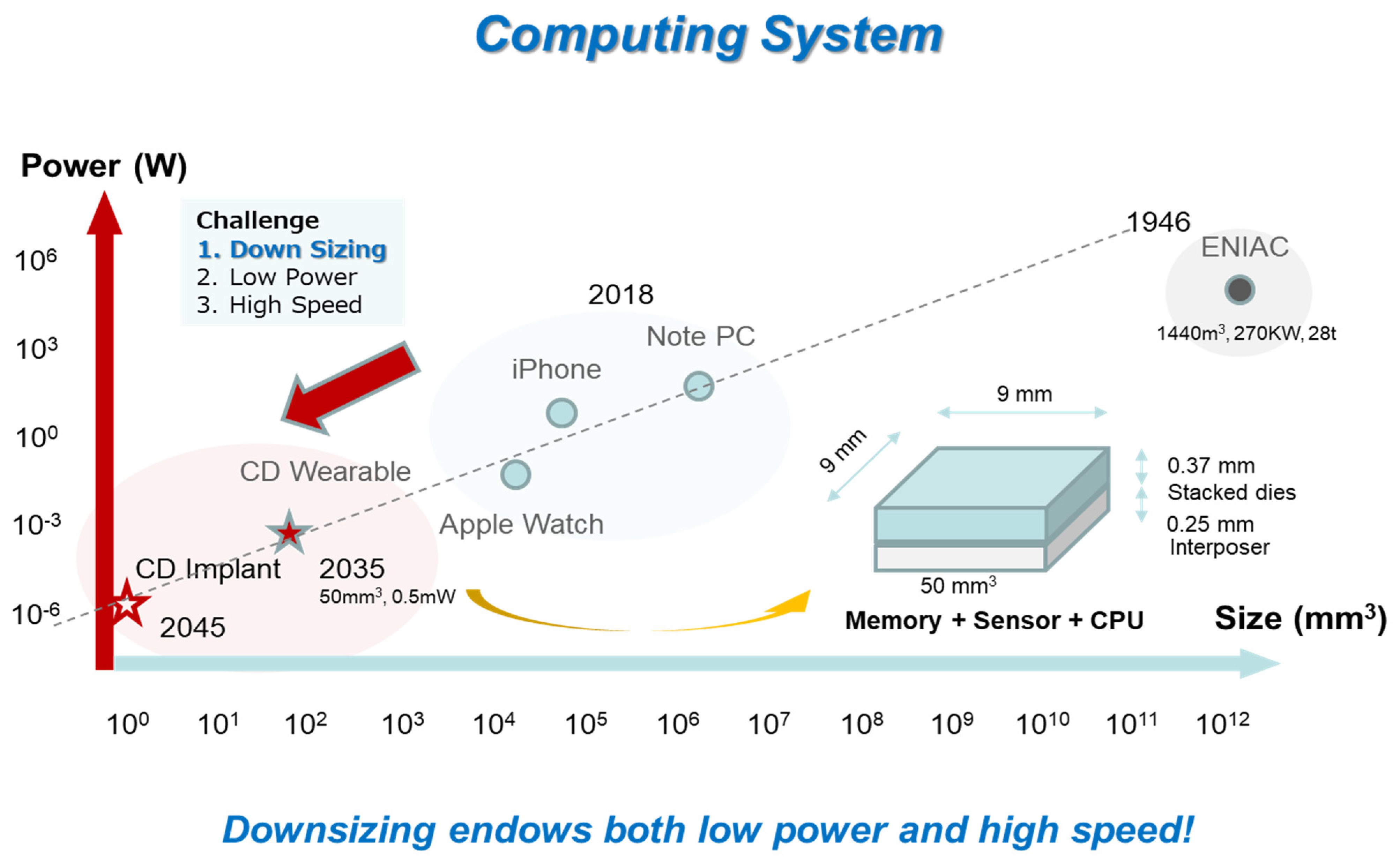
:1. Introduction
2. Manufacturing Cost Crisis for Two-Dimensional Scaling
3. Paradigm Shift to Bumpless Build Cube Integration
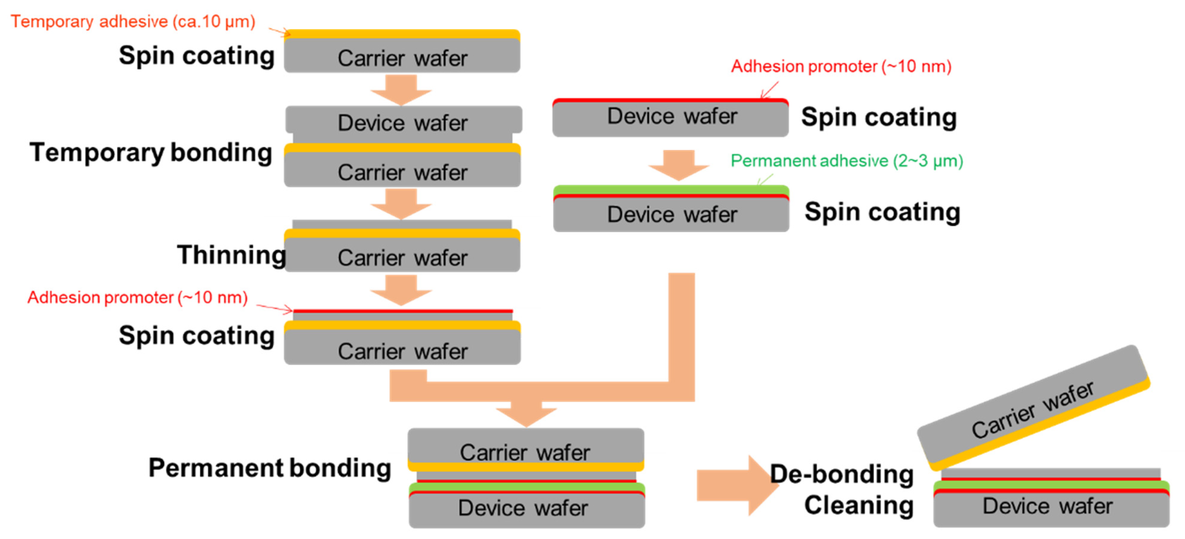
4. Details of BBCube WOW Processes
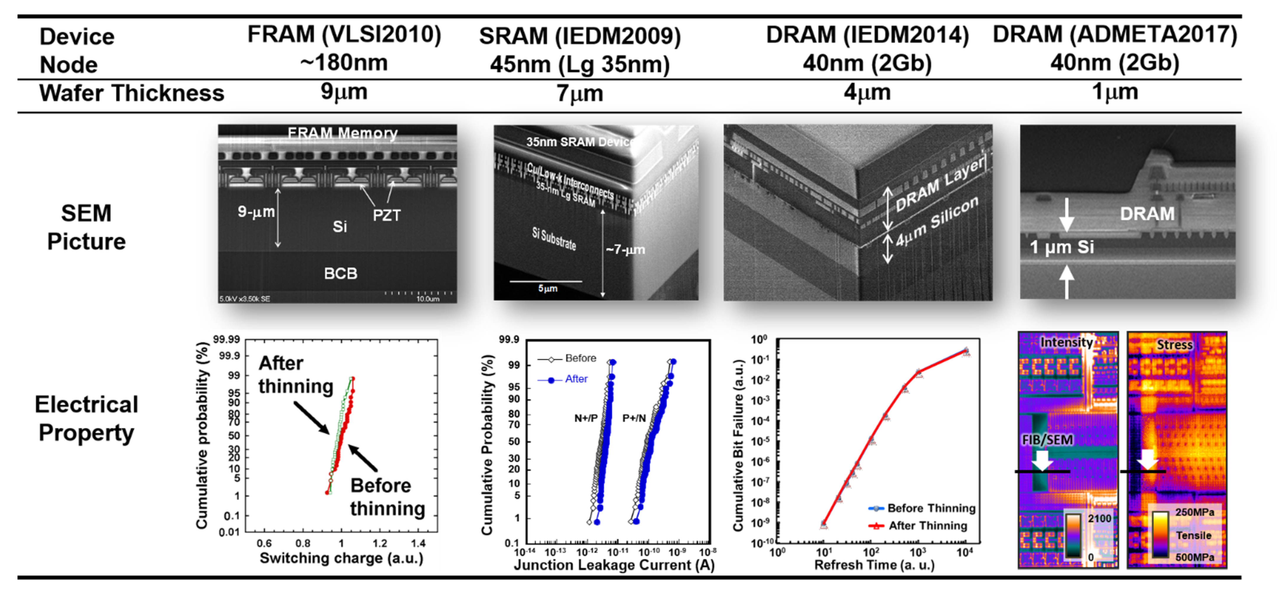
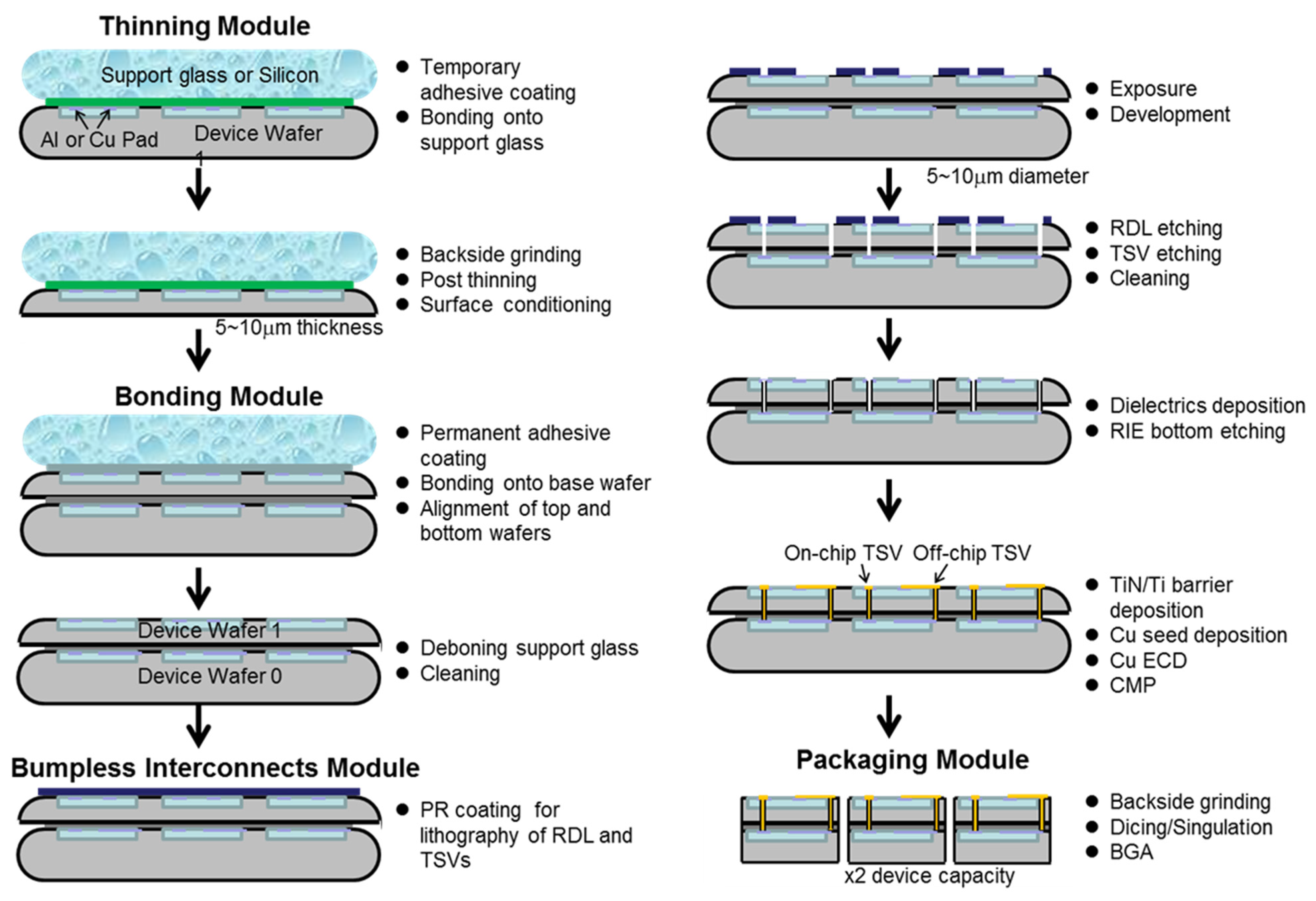
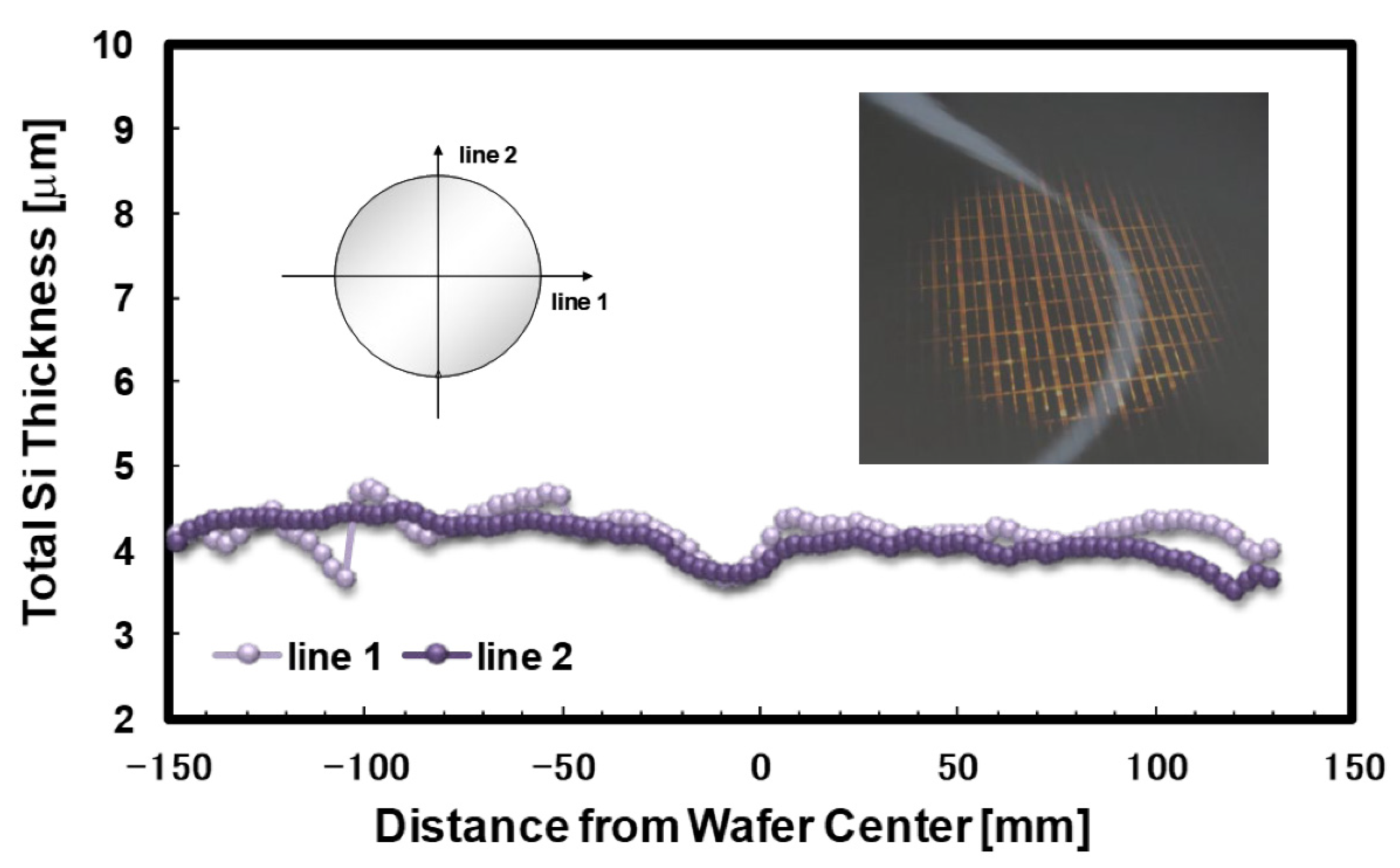
4.1. Thinning Module
4.2. Stacking Module
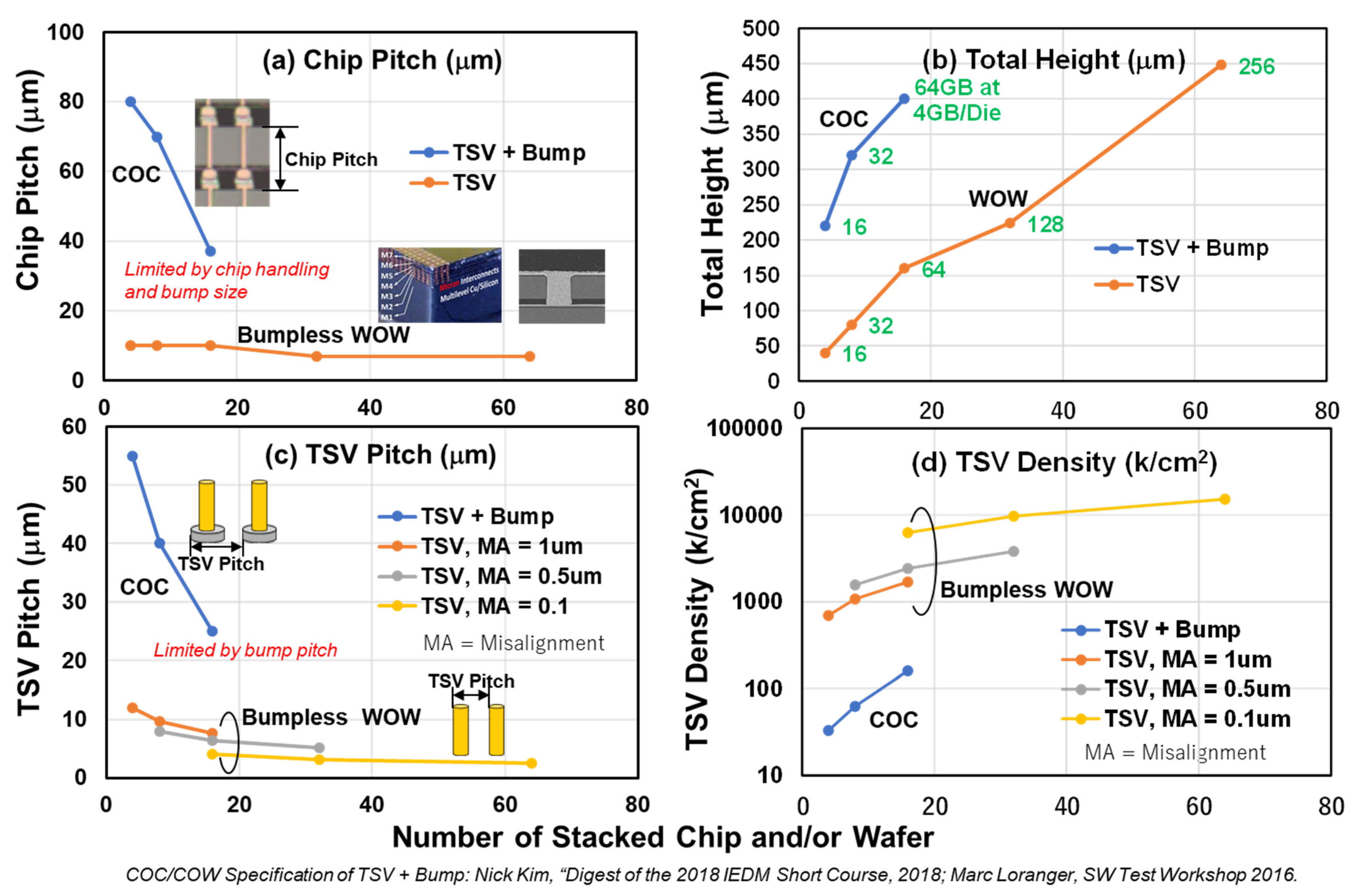
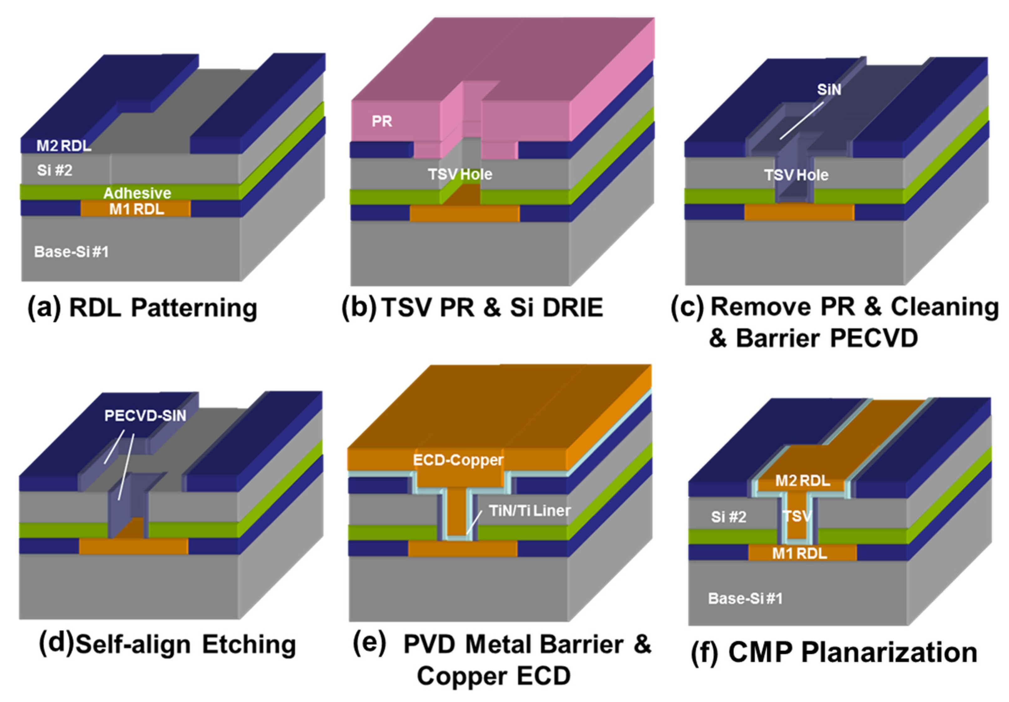
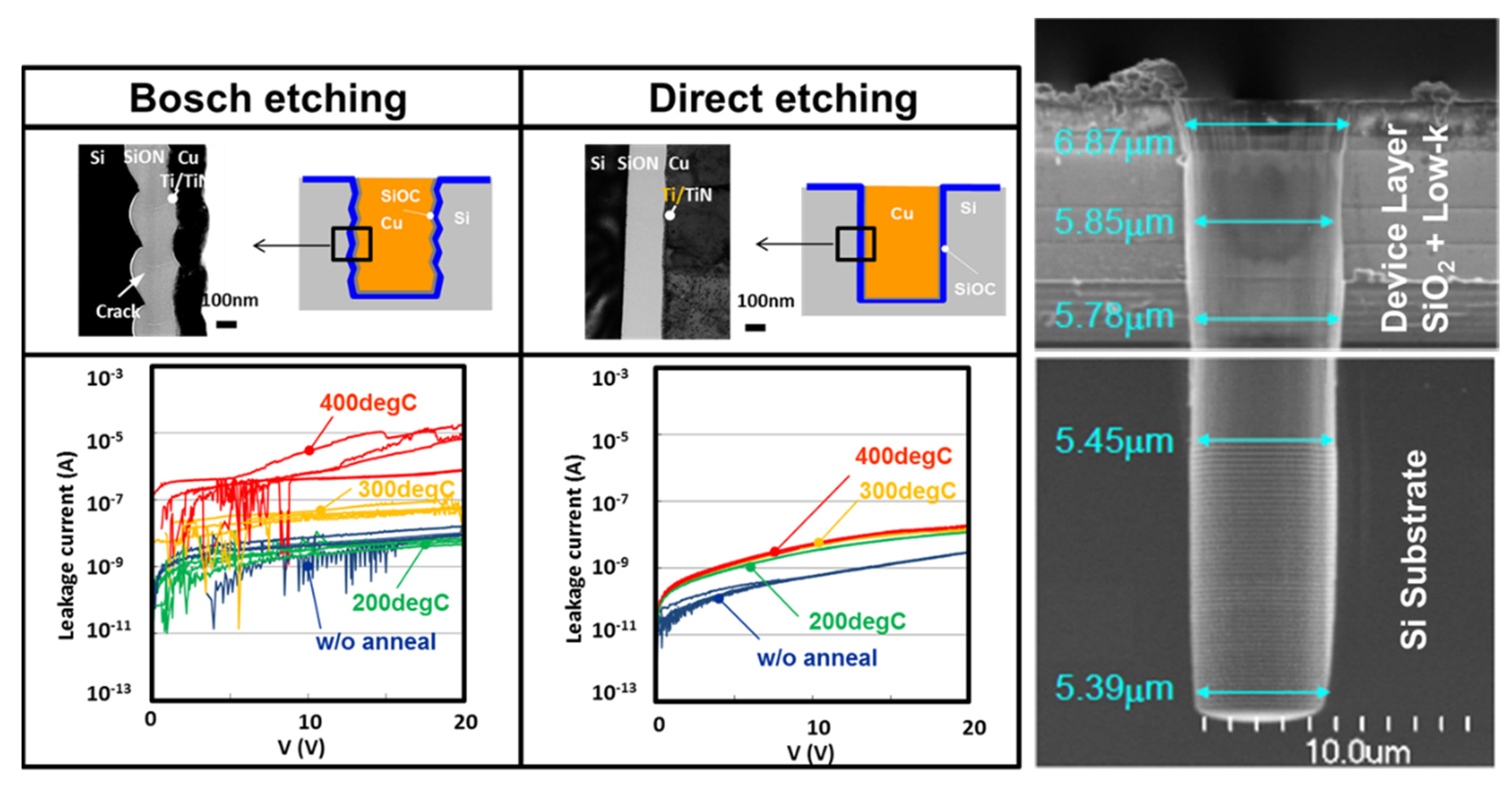
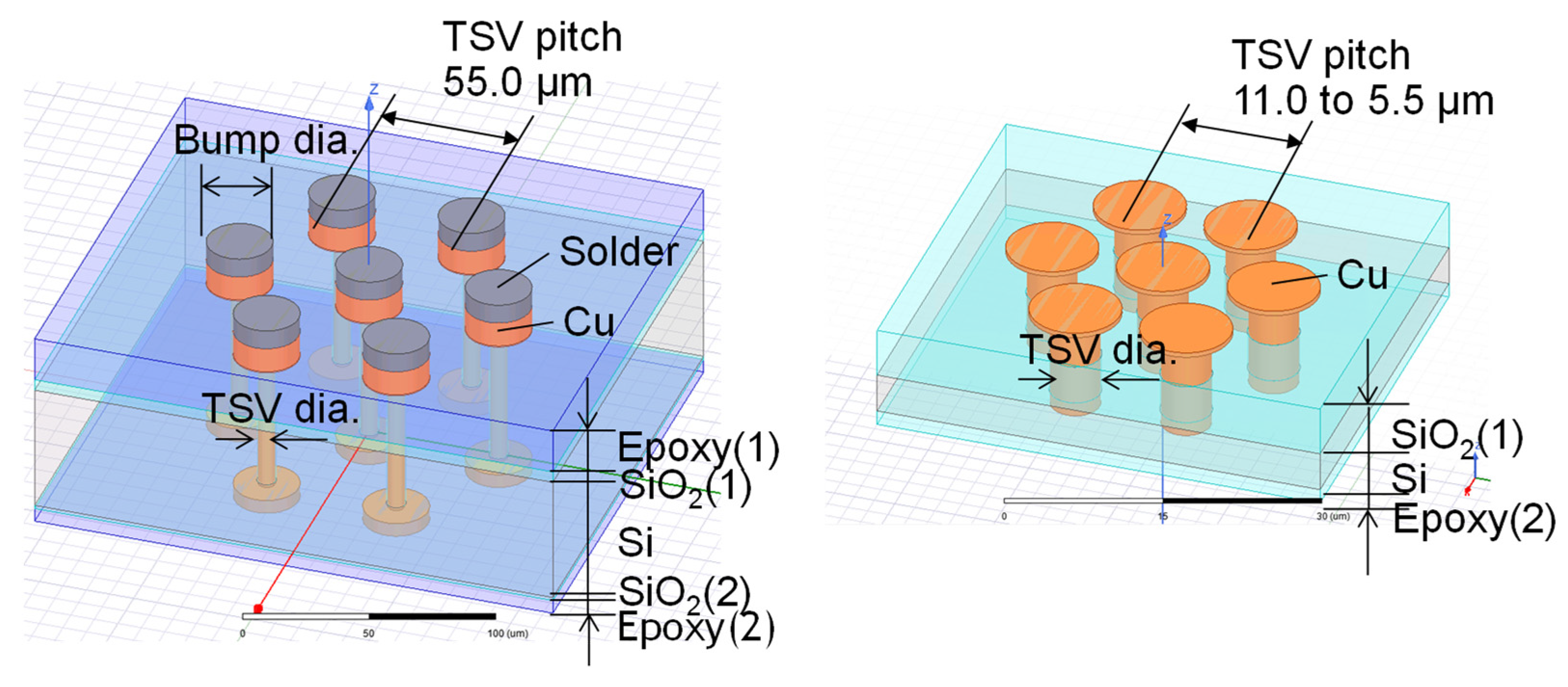
4.3. Through-Silicon-Via (TSV) Module
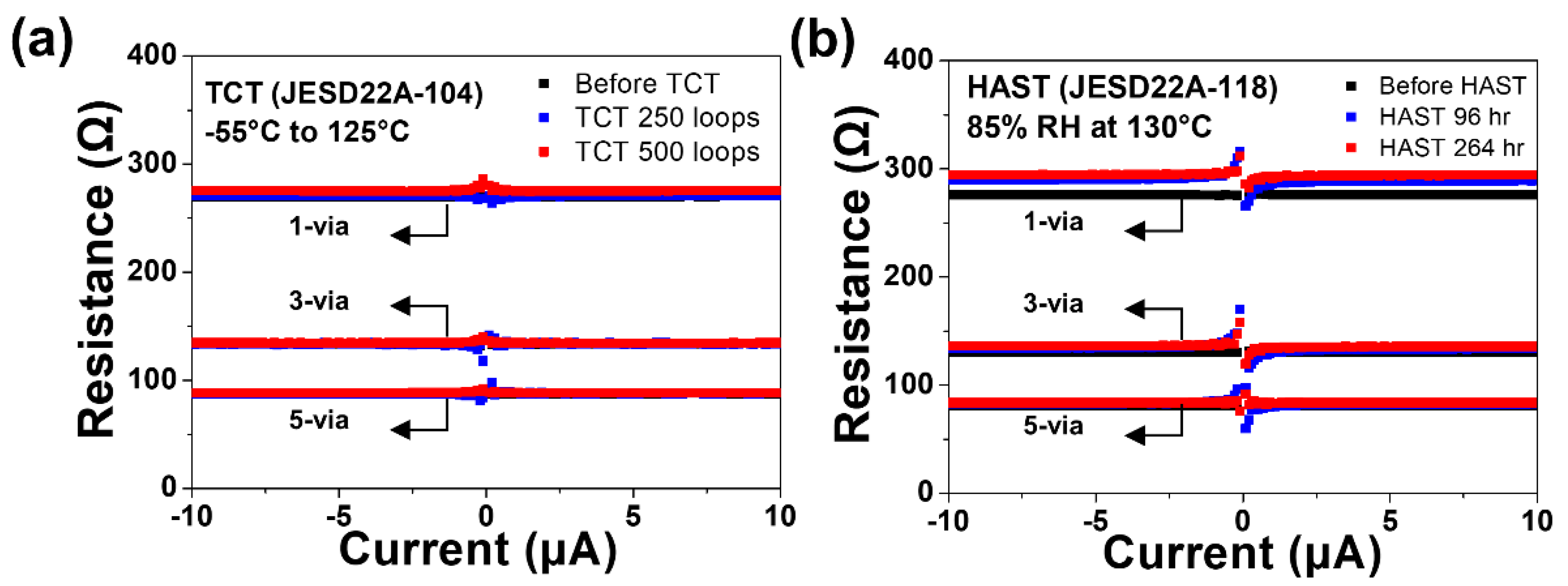
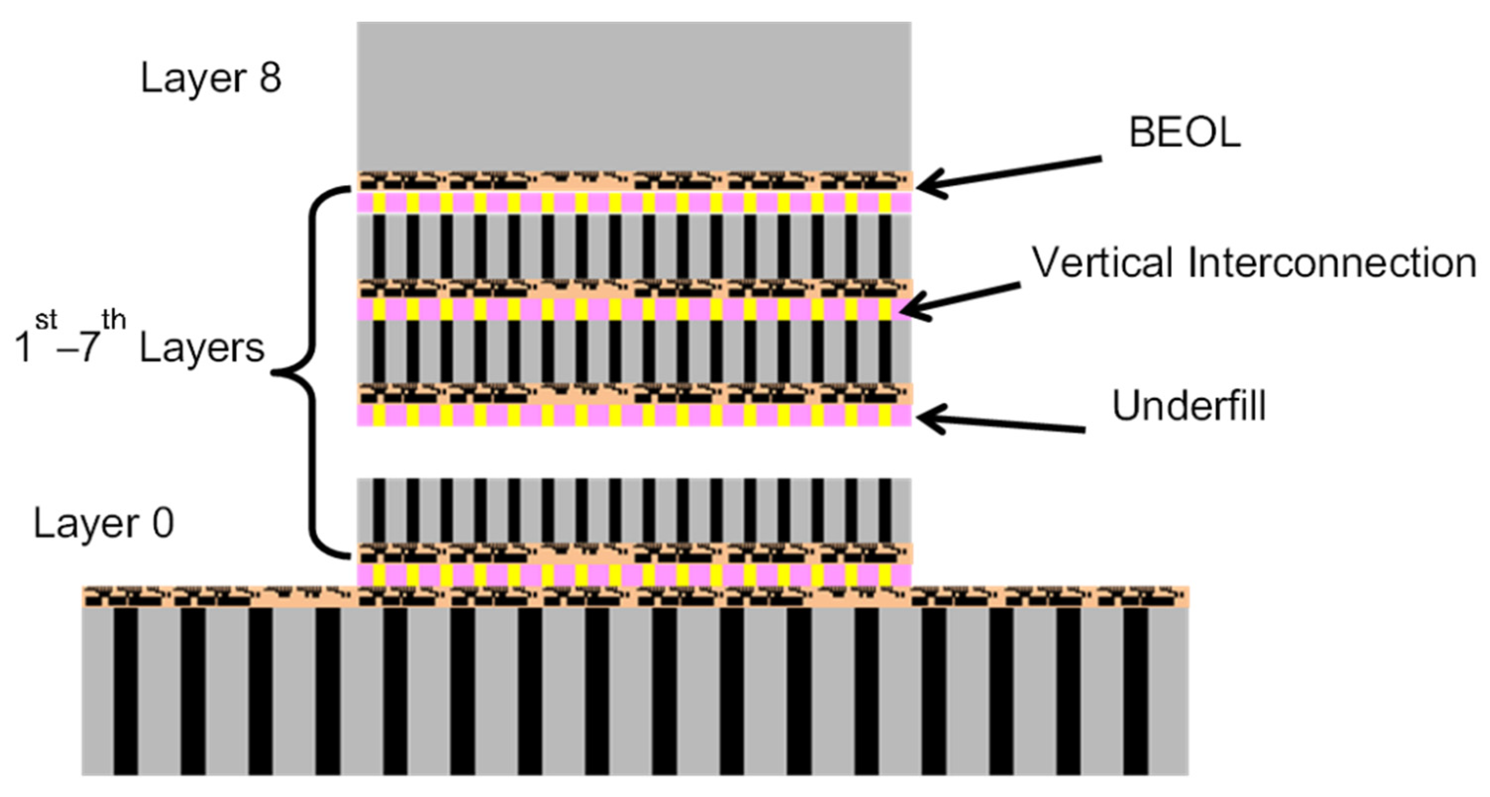
4.4. Singulation/Packaging Module and Reliability
5. BBCube COW Processes
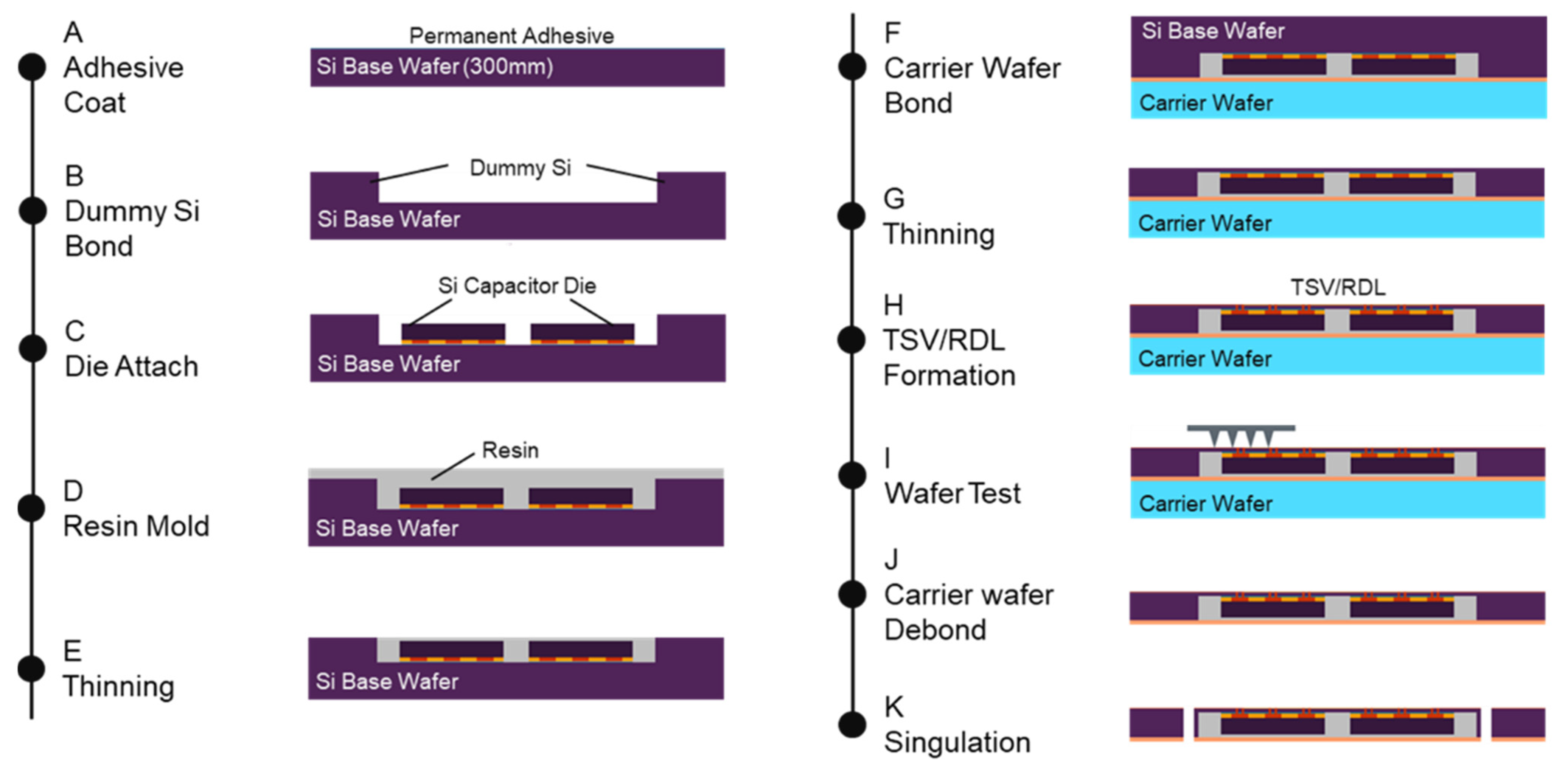
5.1. Heterogenous 3D Integration Process
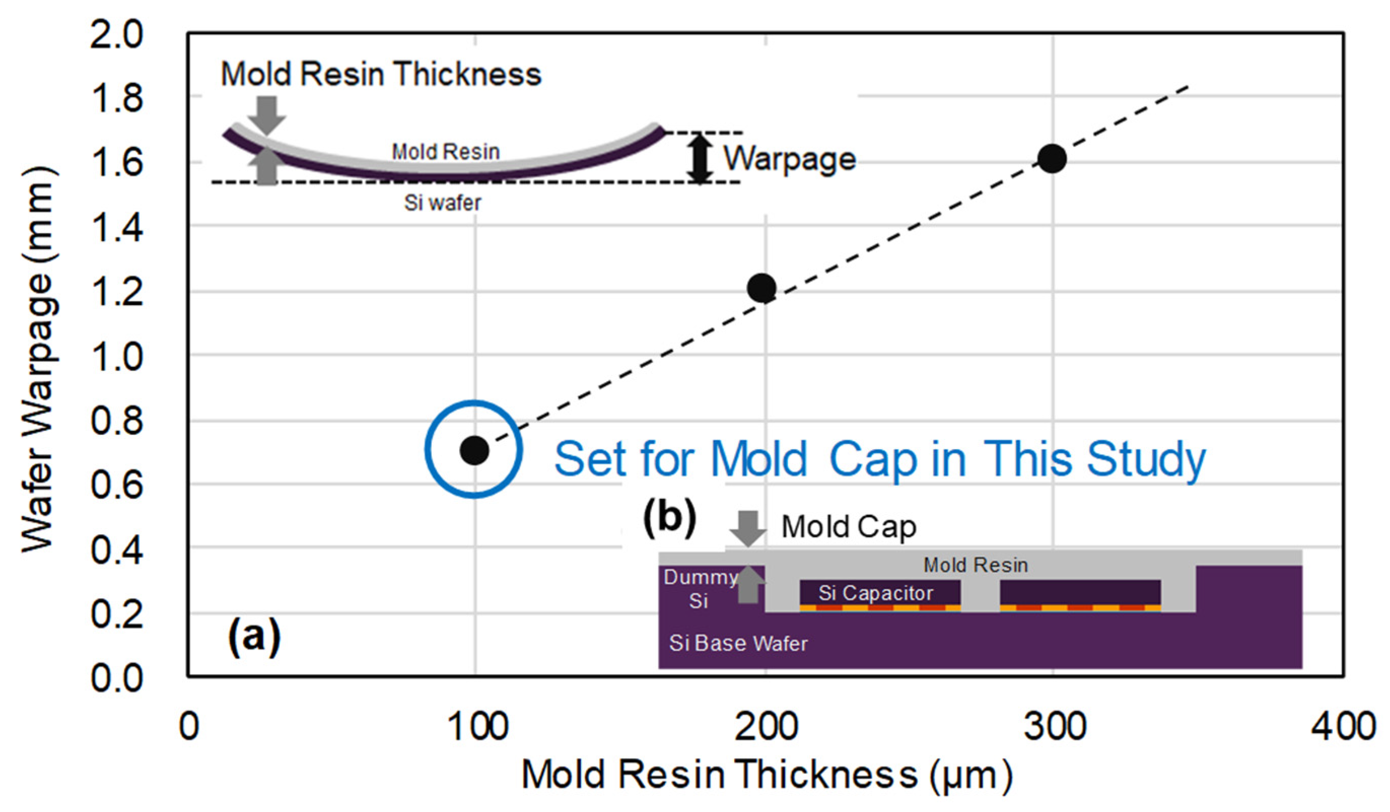
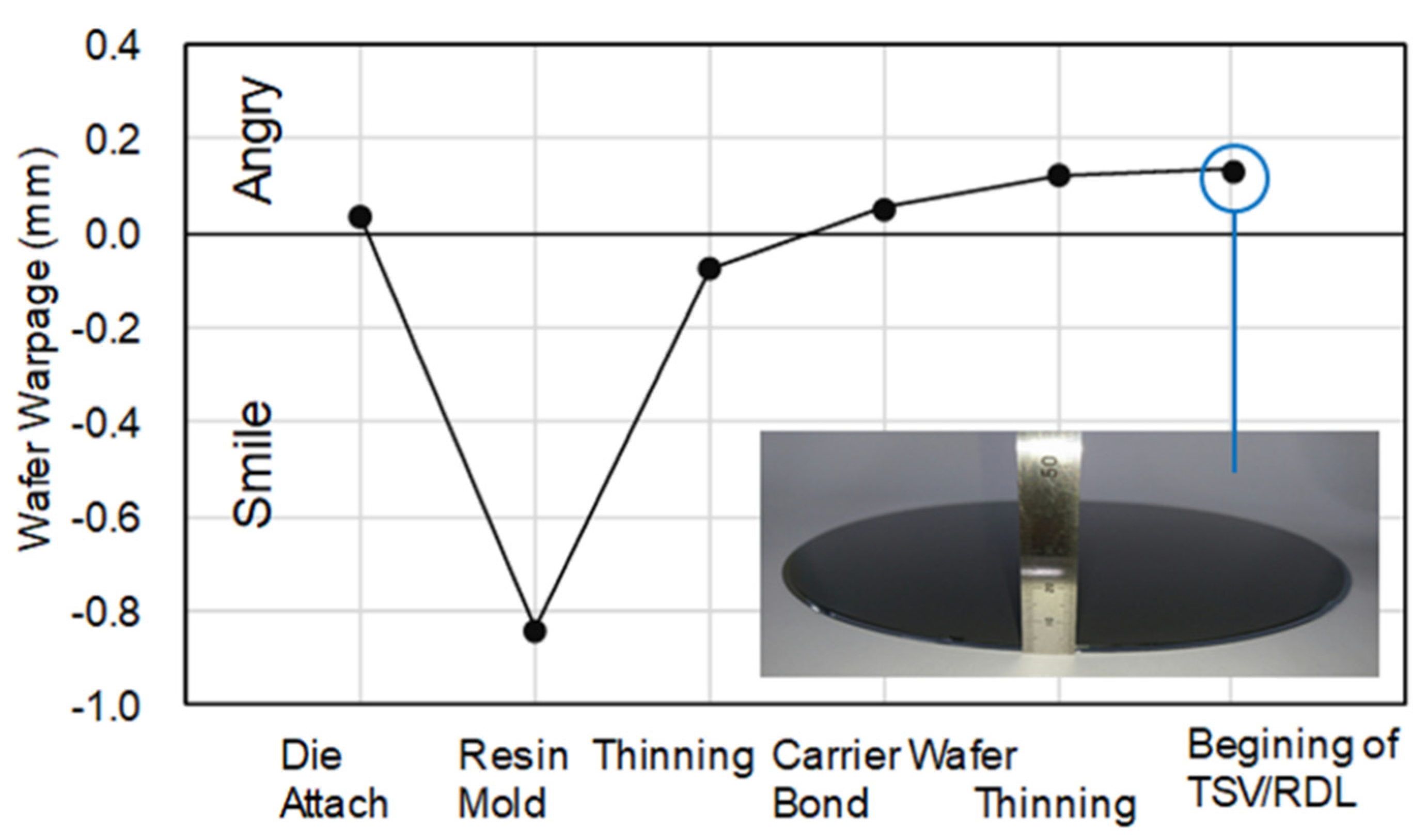
5.2. Wafer Warpage Control
5.3. Accuracy of Die Placement and Reduction of Voids in Adhesive
5.4. Process Sequence of TSV/RDL
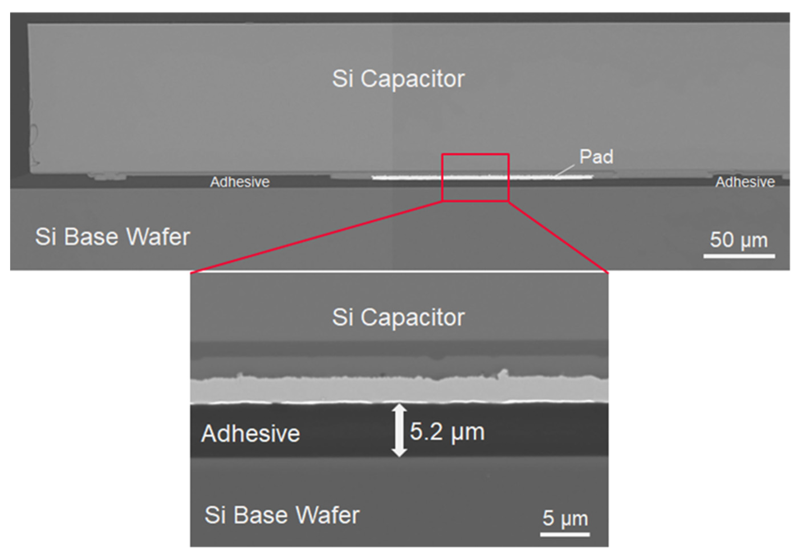
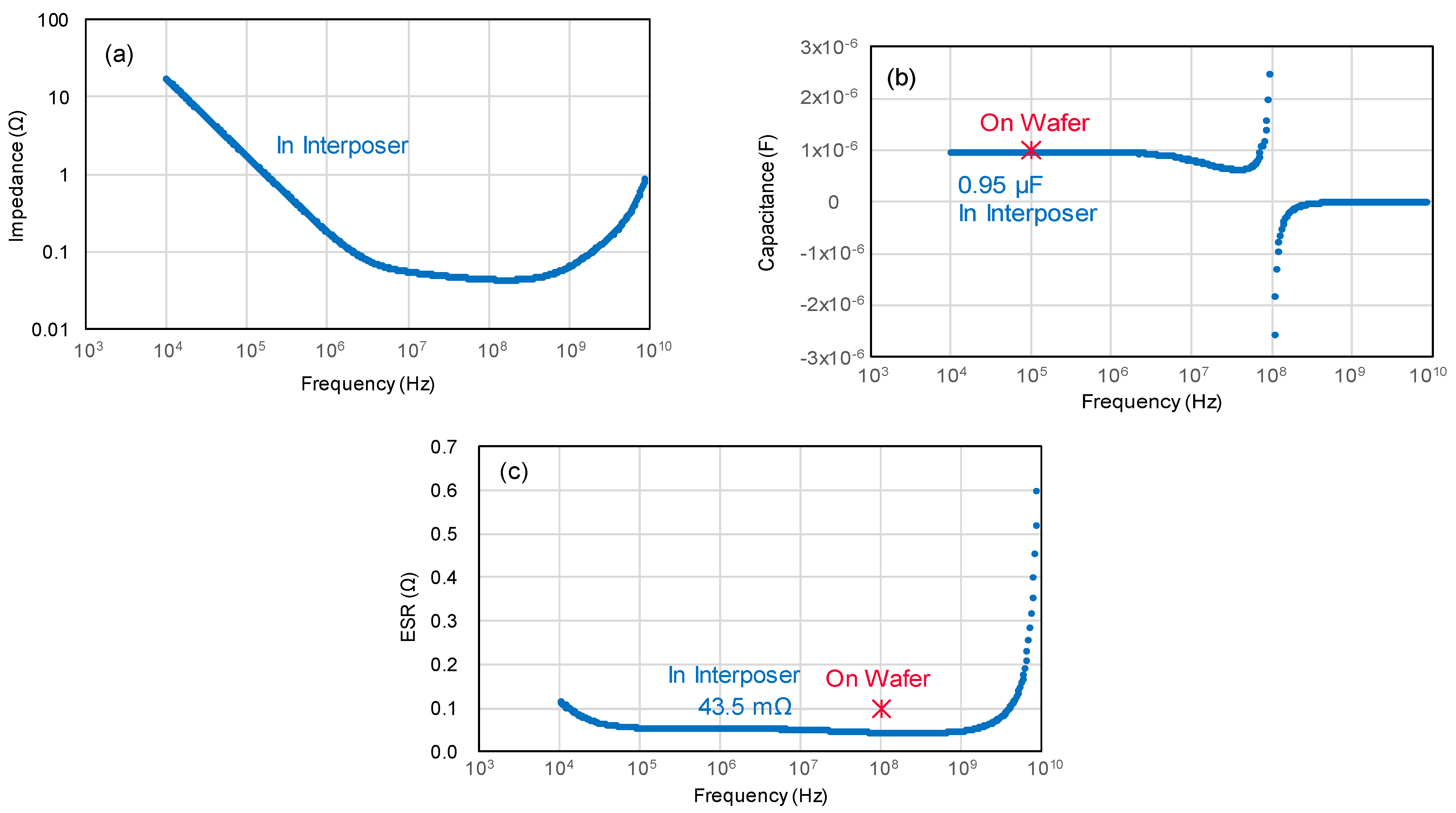
5.5. Electrical Characteristics of Embedded-Si Capacitor in COW
5.6. Benefits and Performance of Bumpless Functional Interposer
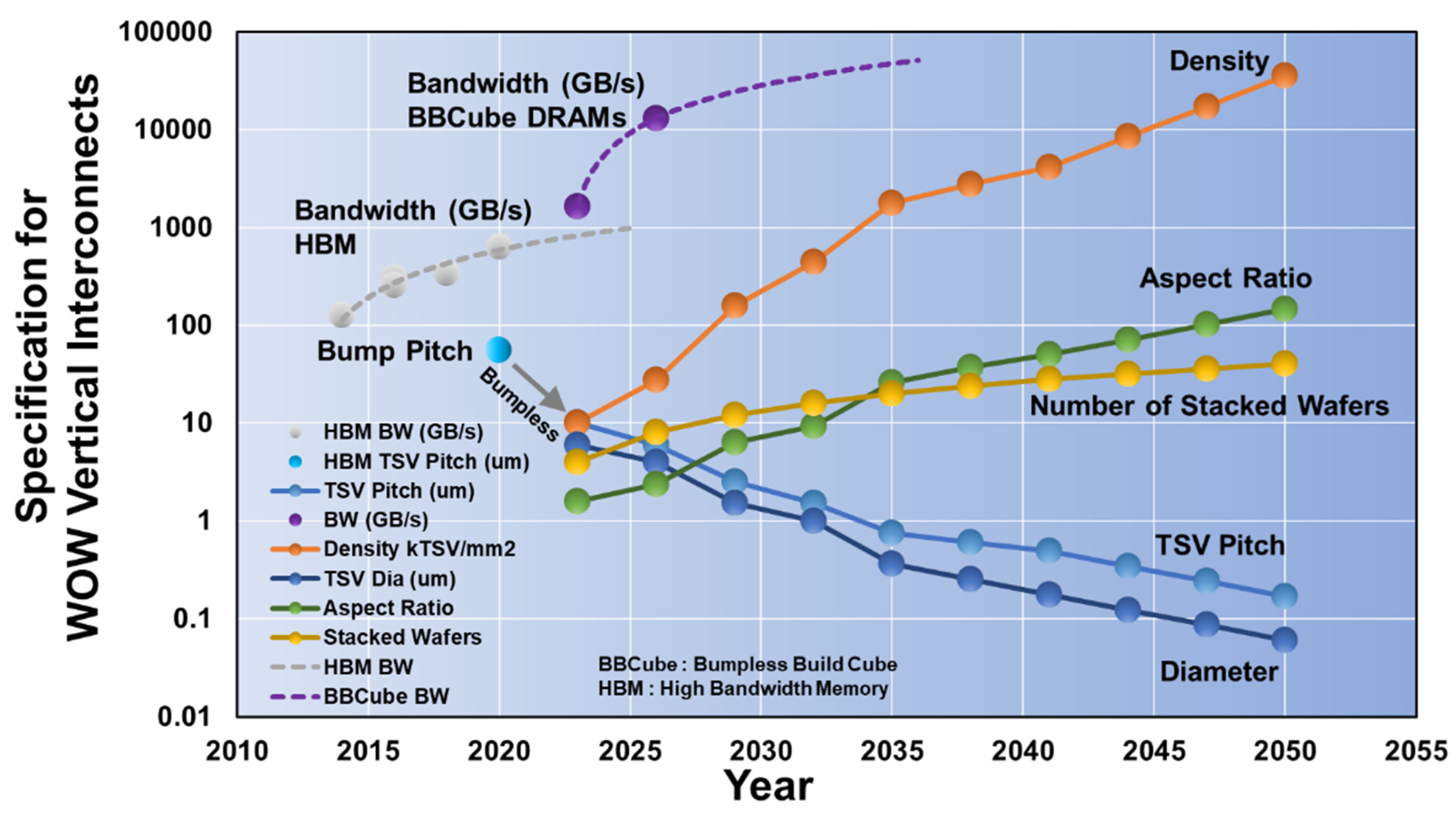
6. BBCube Technology Roadmap
7. BBCube Memory
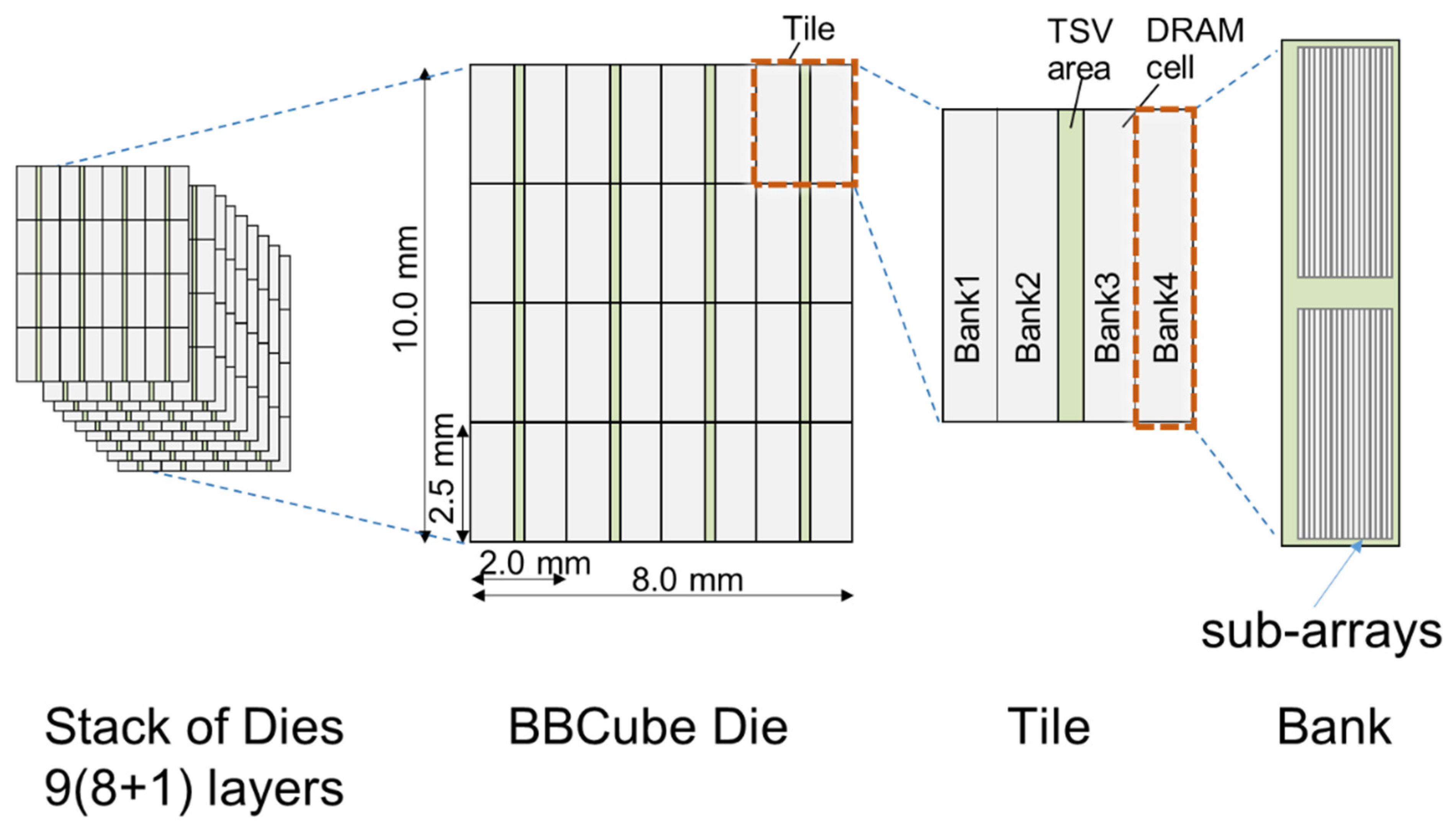
8. BBCube DRAM
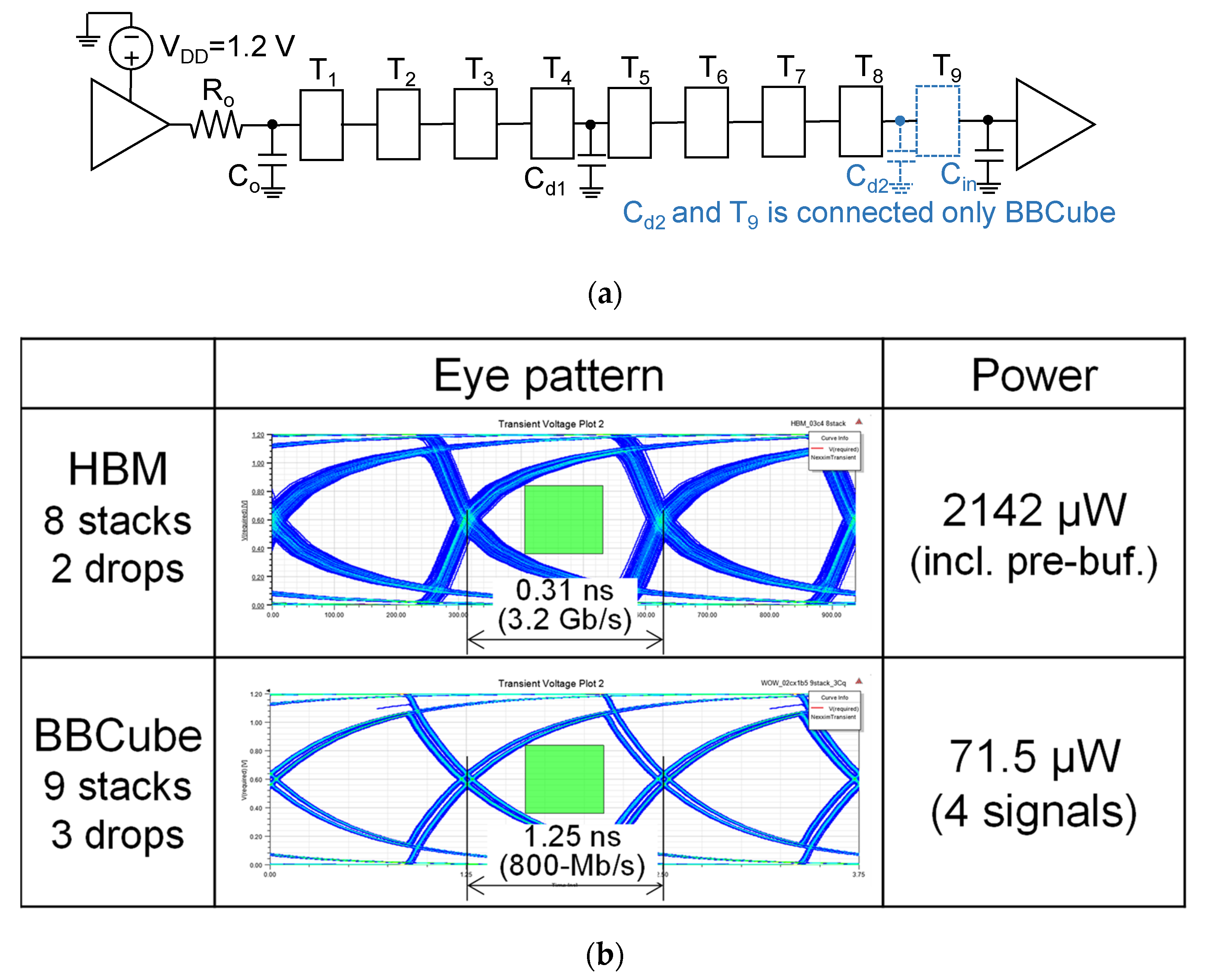
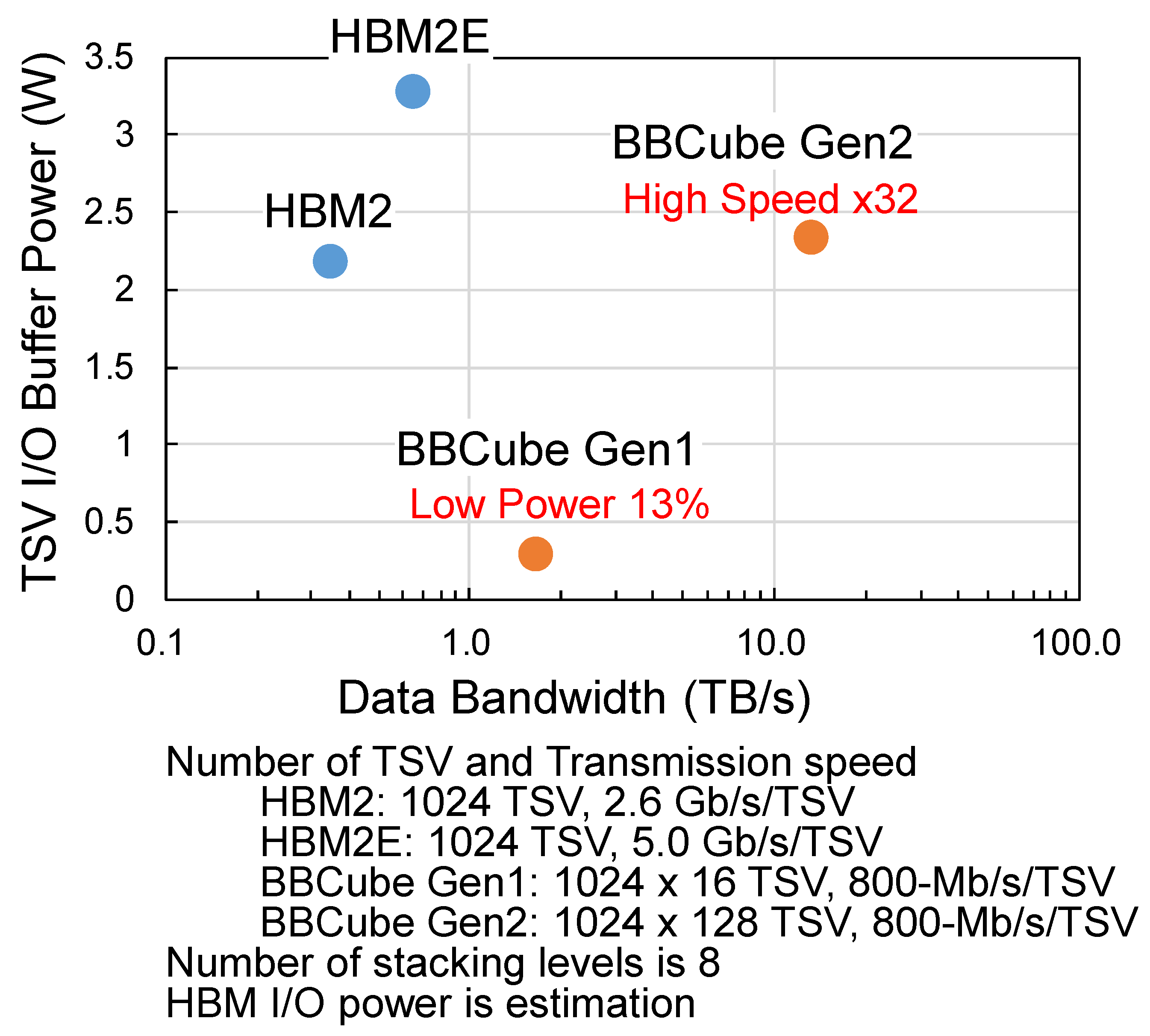
8.1. Electrical Characteristics of BBCube
8.2. Thermal Characteristics of BBCube
8.3. Competitive BBCube DRAM Structure
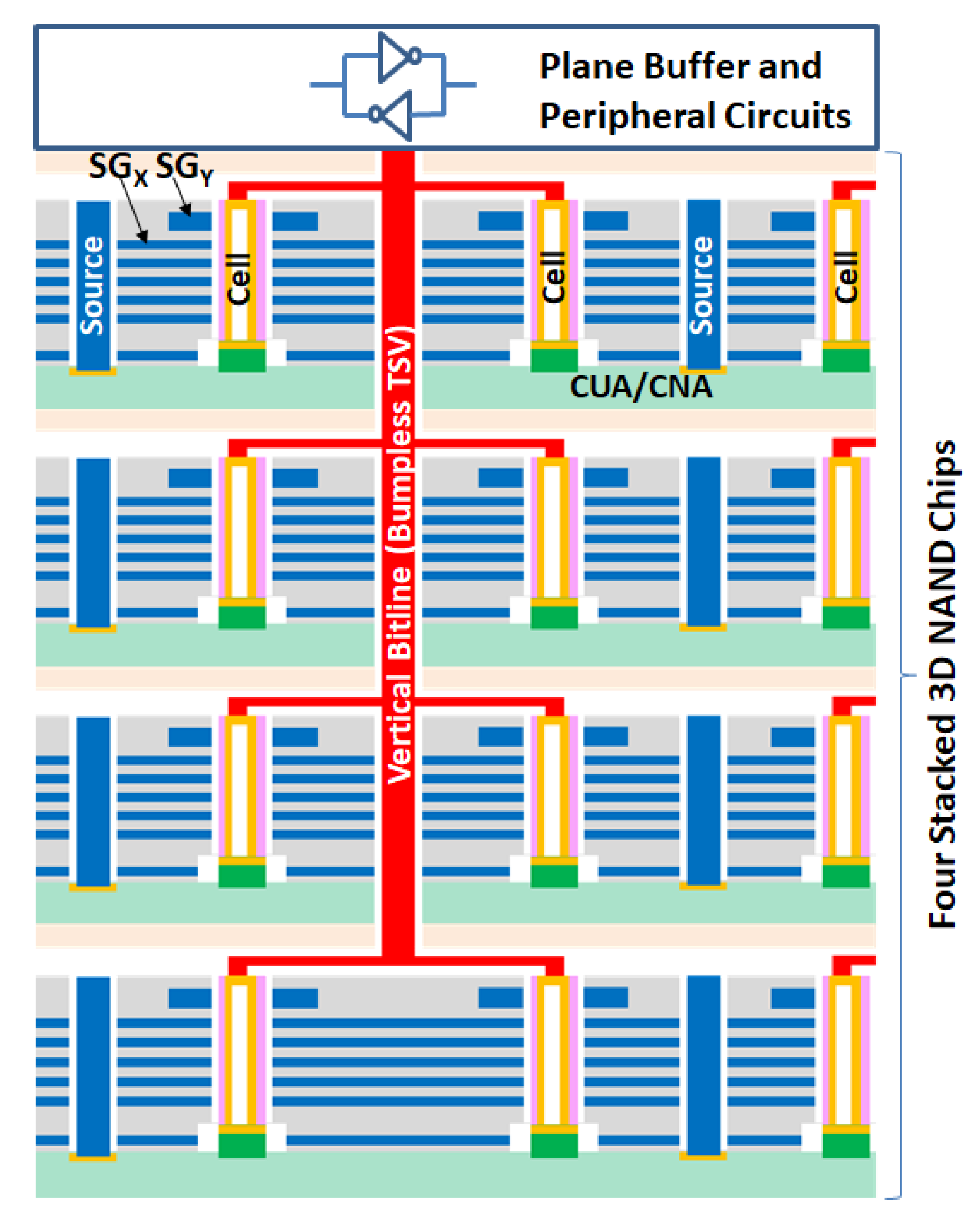
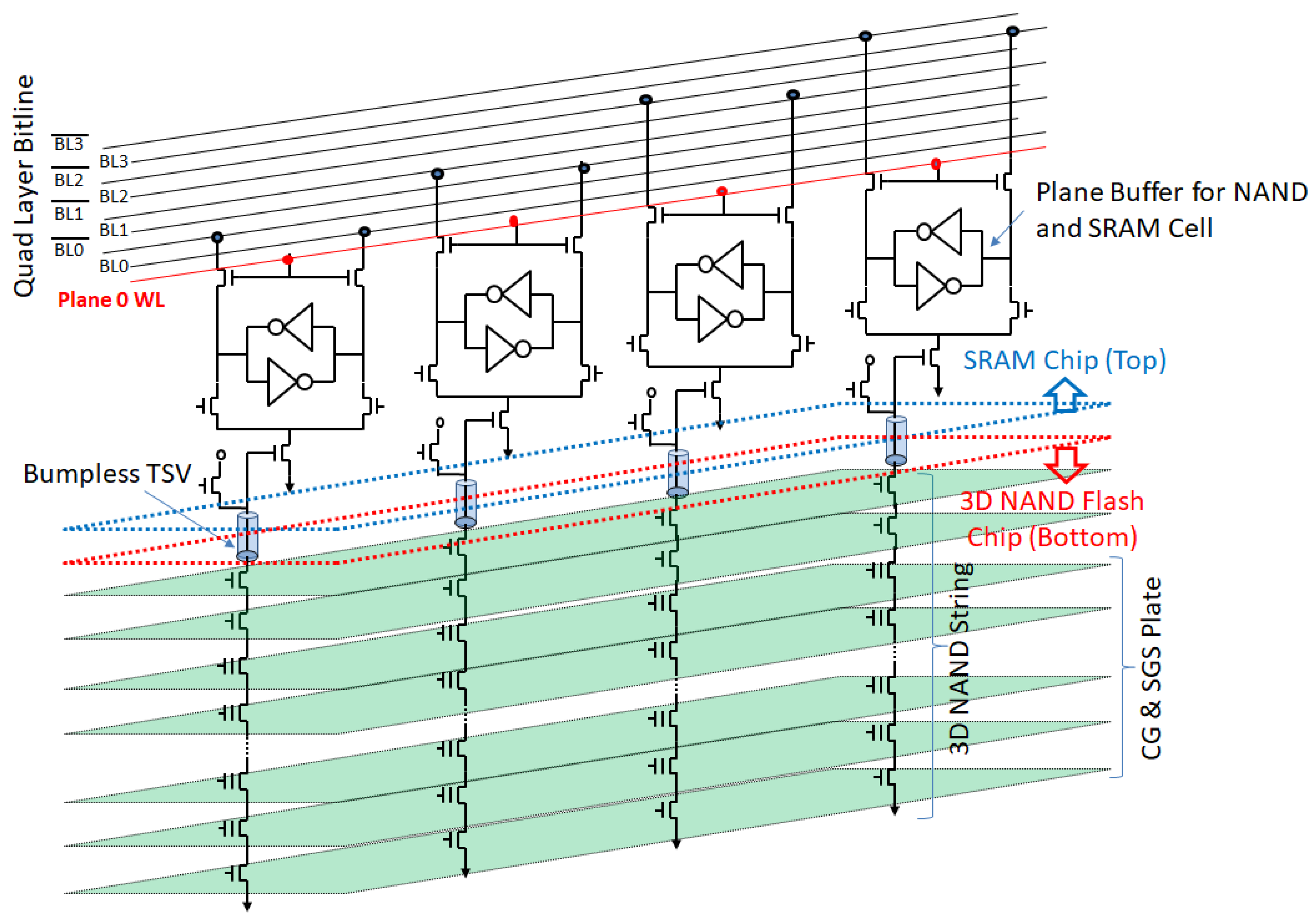
9. BBCube NAND
9.1. Limitations of Stacked WL Tiers in 3D NAND Chip
- i.
- If 64 tiers by one etching shot is limited by the highest aspect ratio, 512 tiers would require 8 times cell process, such as 64 × 8. Therefore, there is a large heat budget to enhance the source/drain diffusion of the transistors for both a CMOS Under Array (CUA) and a CMOS Next Array (CNA). As a result, the peripheral transistors would be very large, and their performance would be degraded.
- ii.
- If the number of cells per string should increase to 128, 256, and beyond, the cell current would be very small, so that random page access would become slower.
- iii.
- In the case of (2), both the page count and block size must be large, which would be user unfriendly for reprogramming, such as data copying and moving.
- iv.
- A solution to the issues in (2) and (3) would be a multiple vertical bitline architecture, but this would make routing and wiring difficult within the tight XY bitline pitch.
- v.
- The number of high-voltage transistors for NAND string drivers must also increase according as the number of stacked WL tiers, which would occupy a huge Si area in spite of the CUA structure.
9.2. Vertical Bitline Architecture
9.3. Word Plate Access NAND
10. BBCube Memory Application
11. Introduction to 3D Redundancy
11.1. Method of 3D Redundancy
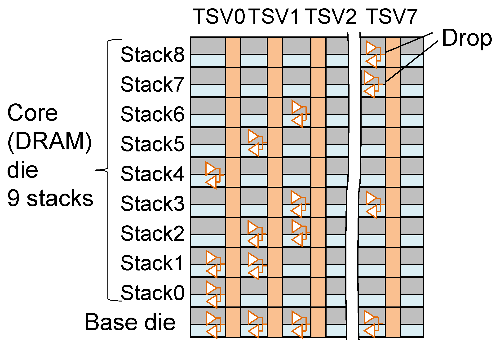
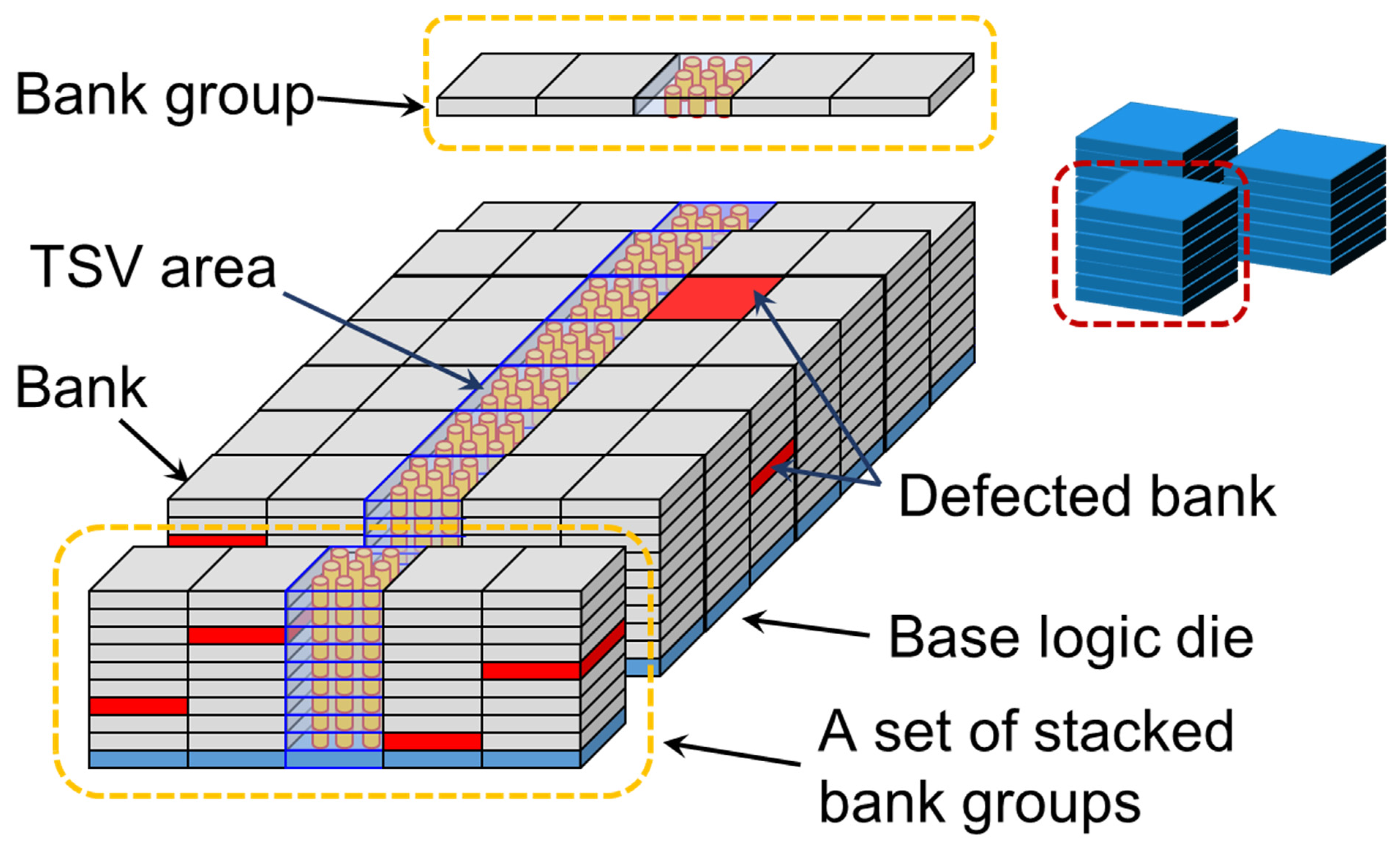
11.1.1. Typical Configuration of Stacked Synchronous DRAM Systems
11.1.2. Techniques for 3D Redundancy
11.1.3. Layer Addition to Cover Circuit Resources
11.1.4. Bank Replacement within a Set of Stacked Bank Groups
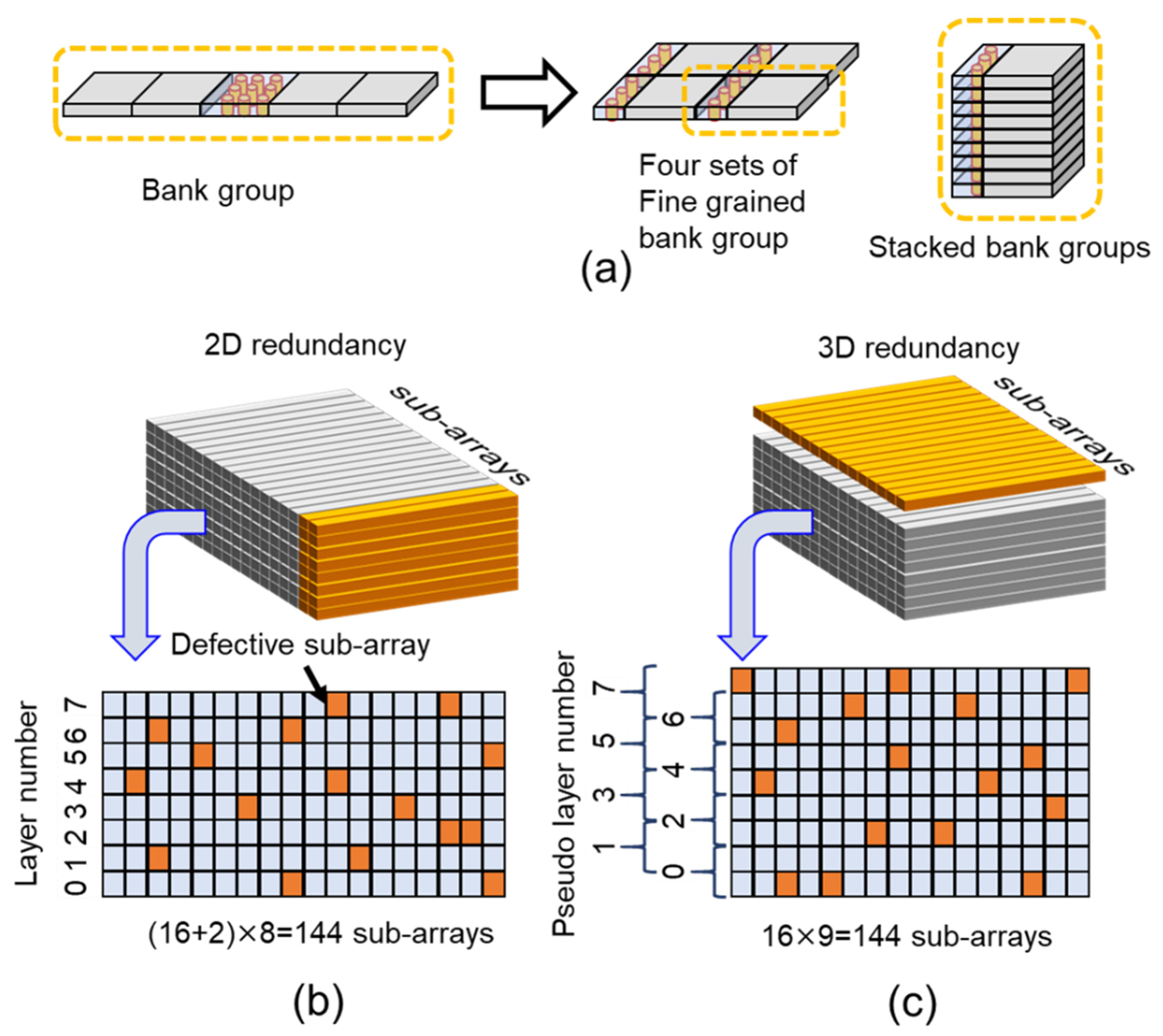
11.1.5. Quasi Layer-by-Layer Operation
11.1.6. Derivative Extension Case: 3D Redundancy at Sub-Array Level
11.1.7. Parameter Definition
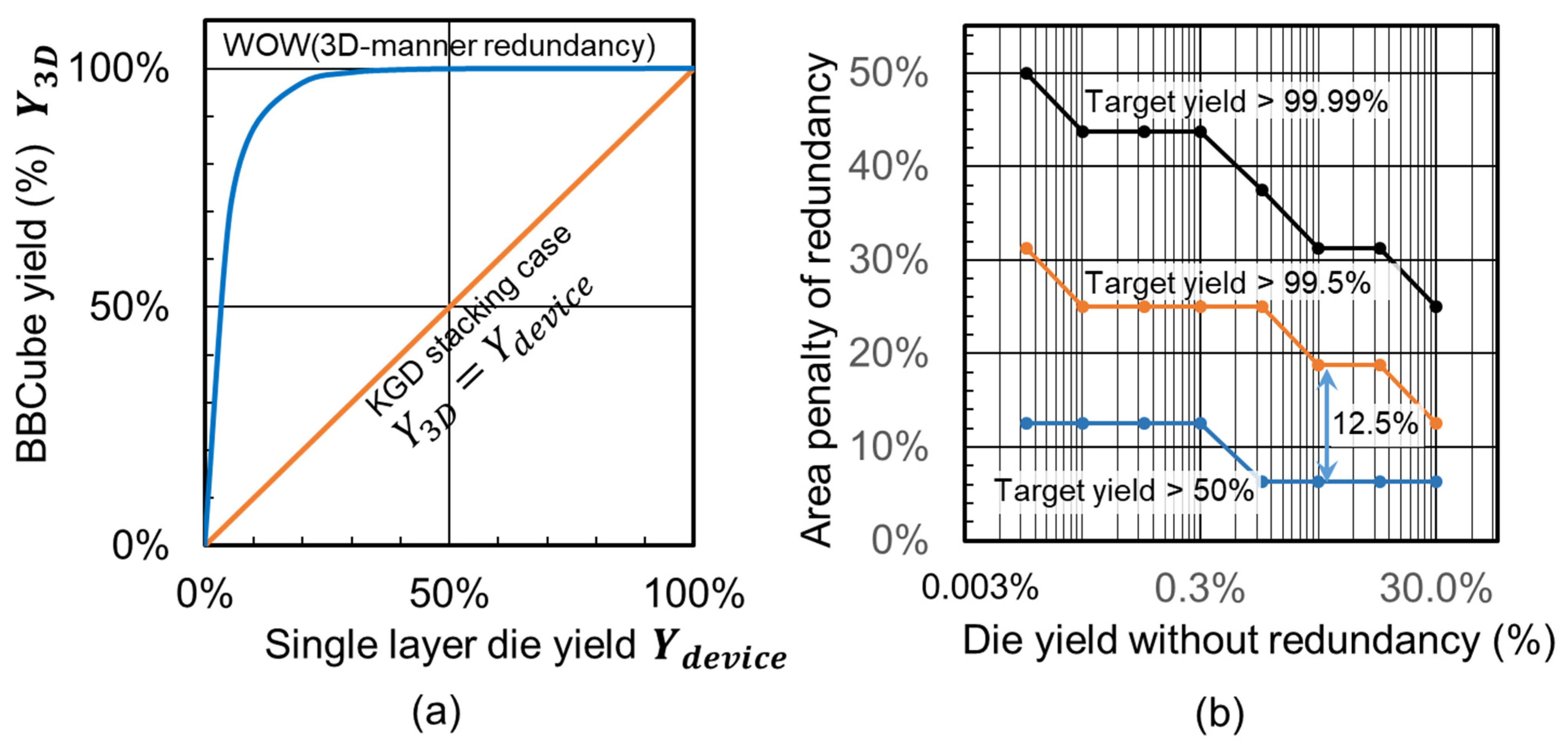
11.1.8. Yield Calculation
11.2. Results and Discussion
11.2.1. Results of BBCube Yield
11.2.2. Discussion
11.3. Conclusion of 3D Redundancy
12. Thermal Resistance Comparison of BBCube and Micro-Bumps
12.1. Thermal Resistance Calculation Method
- i.
- Make assumptions about the IC stack structure,
- ii.
- Estimate the effective thermal conductivity of each layer, and
- iii.
- Calculate thermal resistance of each layer, and
- iv.
- Calculate the temperature rise using the thermal network method.
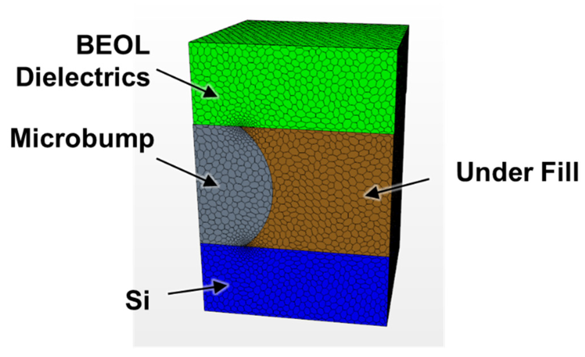
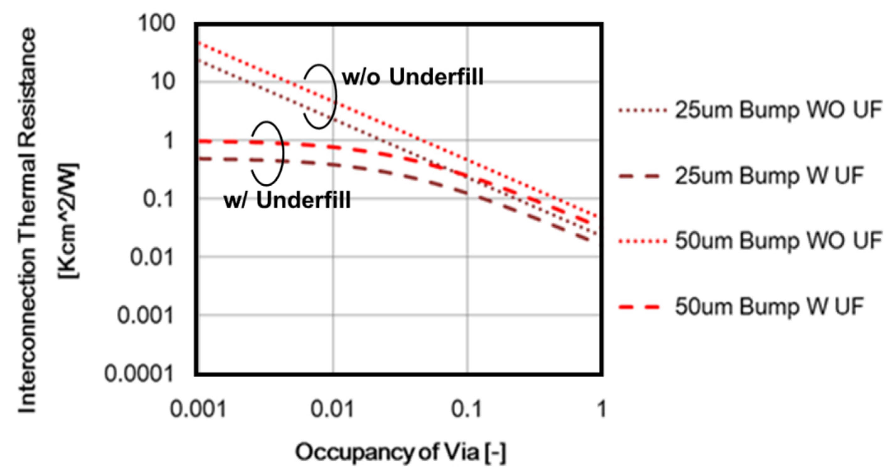
12.2. Thermal Resistance of Micro-Bump Vertical Interconnection
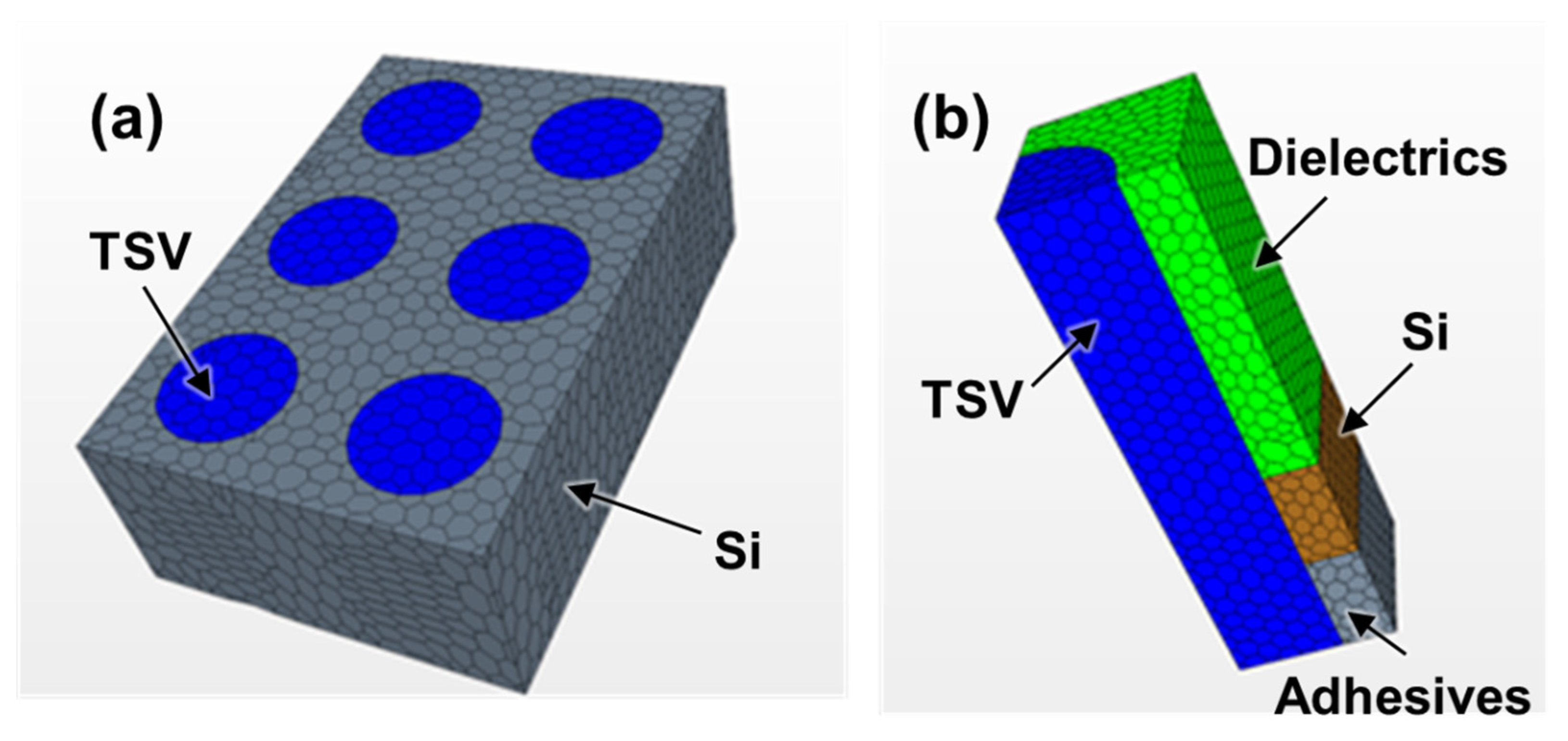
12.3. Thermal Resistance of BBC
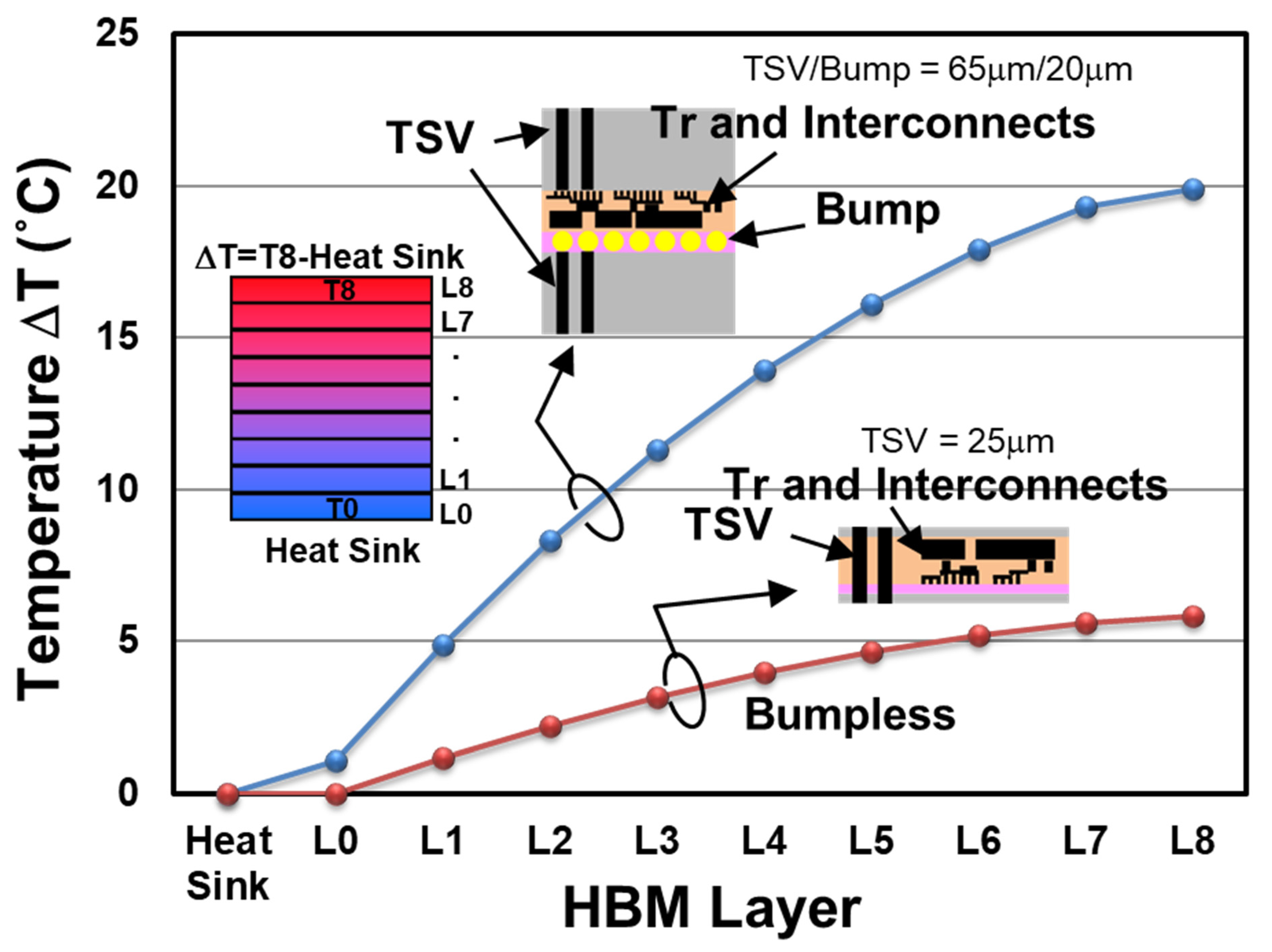
12.4. Temperature Rise Calculation Result
12.5. Thermal Resistance Comparison Conclusion
13. Summary and Conclusions
Author Contributions
Funding
Acknowledgments
Conflicts of Interest
References
- Kilby, J. Miniaturized Electronic Circuits. U.S. Patent 3,138,743, 6 February 1959. [Google Scholar]
- Noyce, R. Semiconductor Device-and-Lead Structure. U.S. Patent 2,981,877, 30 July 1959. [Google Scholar]
- Moore, G. Cramming More Components Onto Integrated Circuits. Electronics 1965, 38, 114–117. [Google Scholar] [CrossRef]
- Dennard, R.H.; Gaensslen, F.H.; Rideout, V.L.; Bassous, E.; LeBlanc, A.R. Design of ion-implanted MOSFET’s with very small physical dimensions. IEEE J. Solid-State Circuit 1974, 9, 256–268. [Google Scholar] [CrossRef] [Green Version]
- Furukawa, S. Three-dimensional Device. J. Inst. Telev. Eng. Jpn. 1982, 36, 1060–1067. [Google Scholar]
- Kurokawa, K.; Aiso, H. Polynomial Transformer. In Proceedings of the 7th Symposium on Computer Arithmetic, Urbana, IL, USA, 4–6 June 1985; IEEE Computer Society Press: Piscataway, NJ, USA, 1985; Volume 7, pp. 153–158. [Google Scholar]
- Nakano, M. Oyo Buturi. Jpn. Soc. Appl. Phys. 1985, 54, 652–659. [Google Scholar]
- Akasaka, Y. Three-Dimensional IC Trends. Proc. IEEE 1986, 74, 1703–1714. [Google Scholar] [CrossRef]
- Spiesshoefer, S.; Schaper, L. IC Stacking Technology Using Fine Pitch Nanoscale Through Silicon Vias. In Proceedings of the 53rd Electronic Components and Technology Conference (ECTC), New Orleans, LA, USA, 27–30 May 2003; pp. 631–633. [Google Scholar]
- Yasumoto, M.; Hayama, H.; Enomoto, T. Promissing New Fabrication Process Developed for Stacked LSI’s. In Proceedings of the 1984 International Electron Devices Meeting, San Francisco, CA, USA, 9–14 December 1984; pp. 816–819. [Google Scholar]
- Hayashi, Y.; Wada, S.; Kajiyana, K.; Oyama, K.; Koh, R.; Takahashi, S.; Kunio, T. Fabrication of Three-Dimensional IC Using ‘CUmulatively Bonded IC’ (CUBIC) Technology. In Proceedings of the Digest of Technical Papers. 1990 Symposium on VLSI Technology, Honololu, HI, USA, 4–7 June 1990; pp. 95–96. [Google Scholar]
- Ramm, P.; Buchner, R. Method of Making a Three-Dimensional Integrated Circuit. U.S. Patent 5,563,084, 8 October 1996. [Google Scholar]
- Ramm, P.; Bollmann, D.; Braun, R.; Buchner, R.; Cao-Minh, U.; Engelhardt, M.; Enmann, G.; Graβ, T.; Hieber, K.; Hübner, H.; et al. Three dimensional metallization for vertically integrated circuits. Microelectron. Eng. 1997, 37, 39–47. [Google Scholar] [CrossRef]
- Matsumoto, T.; Satoh, M.; Sakuma, K.; Kurino, H.; Miyakawa, N.; Itani, H.; Koyanagi, M. New Three-Dimensional Wafer Bonding Technology Using the Adhesive Injection Method. Jpn. J. Appl. Phys. 1998, 1, 1217–1221. [Google Scholar] [CrossRef]
- Tummala, R.; Madisetti, V.K. System on chip or system on package. IEEE Des. Test Comput. 1999, 16, 48–56. [Google Scholar] [CrossRef]
- Lu, J.-Q.; Kumar, A.; Kwon, Y.; Eisenbraun, E.T.; Kraft, R.P.; McDonald, J.F.; Gutmann, R.J.; Cale, T.S.; Belemjain, P.; Erdogan, O.; et al. 3-D Integration Using Wafer Bonding. MRS Proc. Vol. 2001, 16, 515–521. [Google Scholar]
- Shigetou, A.; Itoh, T.; Suga, T. Bumpless Interconnect of Cu Electrodes in Millions-Pins Level. In Proceedings of the IEEE 56th Electronic Components and Technology Conference (ECTC), San Diego, CA, USA, 30 May–2 June 2006; pp. 1003–1008. [Google Scholar]
- Takahashi, K.; Terao, H.; Tomita, Y.; Yamaji, Y.; Hoshino, M.; Sato, T.; Morifuji, T.; Sunohara, M.; Bonkohara, M. Current Status of Research and Development for Three-dimensional Chip Stack Technology. Jpn. J. Appl. Phys. 2001, 40, 3032–3037. [Google Scholar] [CrossRef]
- Klumpp, A.; Merkel, R.; Wieland, R.; Ramm, P. Chip-to-wafer stacking technology for 3D system integration. In Proceedings of the IEEE 53rd Electronic Components and Technology Conference (ECTC), New Orleans, LA, USA, 27–30 May 2003; pp. 1080–1083. [Google Scholar]
- Umemoto, M.; Tanida, K.; Nemoto, Y.; Hoshino, M.; Kojima, M.; Shirai, Y.; Takahashi, K. High-Performance Vertical Interconnection for High-Density 3D Chip Stacking Package. In Proceedings of the IEEE 54rd Electronic Components and Technology Conference (ECTC), Las Vegas, NV, USA, 4 June 2004; pp. 616–623. [Google Scholar]
- Knickerbocker, J.U.; Andry, P.S.; Buchwalter, L.P.; Deutsch, A.; Horton, R.R.; Jenkins, K.A.; Kwark, Y.H.; McVicker, G.; Patel, C.S.; Polastre, R.J.; et al. Development of next-generation system-on-package (SOP) technology based on silicon carriers with fine-pitch chip interconnection. IBM J. Res. Dev. 2005, 49, 725–753. [Google Scholar] [CrossRef] [Green Version]
- Fukushima, T.; Yamada, Y.; Kikuchi, H.; Koyanagi, M. New Three-Dimensional Integration Technology Using Self-Assembly Technique. In Proceedings of the IEEE International Electron Devices Meeting, Washington, DC, USA, 5 December 2005; pp. 359–362. [Google Scholar]
- Tanaka, N.; Yoshimura, Y.; Naito, T.; Miyazaki, C.; Uematsu, T.; Hanada, K.; Toma, N.; Akazawa, T. Low-Cost Through-hole Electrode Interconnection for. 3D-SiP Using Room-temperature Bonding. In Proceedings of the IEEE 56th Electronic Components and Technology Conference (ECTC), San Diego, CA, USA, 30 May–2 June 2006; pp. 814–818. [Google Scholar]
- Brunnbauer, M.; Fürgut, E.; Beer, G.; Meyer, T.; Hedler, H.; Belonio, J.; Nomura, E.; Kiuchi, K.; Kobayashi, K. An Embedded Device Technology Based on a Molded Reconfigured Wafer. In Proceedings of the IEEE 56th Electronic Components and Technology Conference (ECTC), San Diego, CA, USA, 30 May–2 June 2006; pp. 547–551. [Google Scholar]
- Topol, A.W.; la Tulipe, D.C.; Shi, L.; Frank, D.J.; Bernstein, K.; Steen, S.E.; Kumar, A.; Singco, G.U.; Young, A.M.; Guarini, K.W.; et al. Three-Dimensional Integrated Circuits. IBM J. Res. Dev. 2006, 50, 491–506. [Google Scholar] [CrossRef]
- Burns, J.A.; Aull, B.F.; Chen, C.K.; Chen, C.-L.; Keast, C.L.; Knecht, J.M.; Suntharalingam, V.; Warner, K.; Wyatt, P.W.; Yost, D.-R.W. A Wafer-Scale 3-D Circuit Integration Technology. IEEE Trans. Elect. Dev. 2006, 53, 2507–2516. [Google Scholar] [CrossRef]
- Miyakawa, N.; Hashimoto, E.; Maebashi, T.; Nakamura, N.; Sacho, Y.; Nakayama, S.; Toyoda, S. Multilayer stacking technology using wafer-to-wafer stacked method. ACM J. Emerg. Technol. Comput. Syst. 2008, 4, 1–15. [Google Scholar] [CrossRef]
- Sakui, K.; Ohba, T. Three-dimensional Integration (3DI) with Bumpless Interconnects for Tera-scale Generation—High Speed, Low Power, and Ultra-small Operating Platform. In Proceedings of the 2019 IEEE Custom Integrated Circuits Conference (CICC), Austin, TX, USA, 14–17 April 2019; pp. 22–26. [Google Scholar]
- Sakui, K.; Ohba, T. High Speed, Low Power, and Ultra-small Operating Platform with Three-dimensional Integration (3DI) by Bumpless Interconnects. In Proceedings of the IEEE 11th International Memory Workshop (IMW), Monterey, CA, USA, 12–15 May 2019; pp. 60–63. [Google Scholar]
- Kim, J.-S.; Oh, C.S.; Lee, H.; Lee, D.; Hwang, H.-R.; Hwang, S.; Na, B.; Moon, J.; Kim, J.-G.; Park, H.; et al. A 1.2V 12.8GB/s 2Gb Mobile Wide-I/O DRAM with 4 × 128 I/Os Using TSV-Based Stacking. IEEE J. Solid-State Circuits 2012, 47, 107–116. [Google Scholar] [CrossRef]
- Ohba, T.; Maeda, N.; Kitada, H.; Fujimoto, K.; Suzuki, K.; Nakamura, T.; Kawai, A.; Arai, K. Thinned Wafer Multi-stack 3DI Technology. Microelectron. Eng. 2010, 87, 485–490. [Google Scholar] [CrossRef]
- Ohba, T. Three-Dimensional (3D) Integration Technology. Electrochem. Soc. Trans. 2011, 34, 1011–1016. [Google Scholar] [CrossRef]
- Ohba, T.; Kim, Y.S.; Mizushima, Y.; Maeda, N.; Fujimoto, K.; Kodama, S. Review of Wafer-Level Three-Dimensional Integration (3DI) using Bumpless Interconnects for Tera-Scale Generation. IEICE Electron. Express 2015, 12, 1–14. [Google Scholar] [CrossRef] [Green Version]
- Chujo, N.; Sakui, K.; Ryoson, H.; Sugatani, S.; Nakamura, T.; Ohba, T. Bumpless Build Cube (BBCube): High-Parallelism, High-Heat-Dissipation and Low-Power Stacked Memory Using Wafer-Level 3D Integration Process. In Proceedings of the 2020 IEEE Symposium on VLSI Technology, Honolulu, HI, USA, 16–19 June 2020. [Google Scholar]
- Helms, C.R. Semiconductor Technology & Manufacturing Status, Challenges, and Solutions—A New Paradigm in the Making. AIP Conf. Proc. 2003, 683, 63–73. [Google Scholar]
- Available online: https://www.semi.org/en/semiconductor-industry-2015-2025 (accessed on 25 December 2021).
- Green, D.S. DARPA’s CHIPS Program, and Making Heterogeneous Integration Common. In Proceedings of the 14th Annual Conference on 3D Architectures for Semiconductor Integration and Packaging (3D-ASIP), San Francisco, CA, USA, 5–7 December 2017; Available online: https://www.darpa.mil/news-events/2016-07-19 (accessed on 25 December 2021).
- Su, L.T.; Naffziger, S.; Papermaster, M. Multi-Chip Technologies to Unleash Computing Performance Gains over the Next Decade. In Proceedings of the 2017 IEEE International Electron Devices Meeting (IEDM), San Francisco, CA, USA, 2–6 December 2017; pp. 1–8. [Google Scholar]
- Available online: https://www.brookings.edu/techstream/the-chip-making-machine-at-the-center-of-chinese-dual-use-concerns/ (accessed on 25 December 2021).
- Schoenfelder, S.; Ebert, M.; Landesberger, C.; Bock, K.; Bagdahn, J. Investigations of The Influence of Dicing Techniques on the Strength Properties of Thin Silicon. Microelectron. Reliab. 2007, 47, 168–178. [Google Scholar] [CrossRef]
- Huang, P.S.; Tsai, M.Y. Nonlinearities in Thin-Silicon Die Strength Tests. In Proceedings of the International Microsystems, Packaging, Assembly and Circuits Technology Conference (IMPACT), Taipei, Taiwan, 19–21 October 2011; pp. 91–95. [Google Scholar]
- Ohba, T. Multilevel Interconnect Technologies in SoC and SiP for 100-nm Node and Beyond. In Proceedings of the IEEE 6th International Conference on Solid-State Integrated Circuit Technology (ICSICT), Shanghai, China, 22–25 October 2001; pp. 46–51. [Google Scholar]
- Wang, G.; Merrill, C.; Zhao, J.H.; Groothuis, S.K.; Ho, P.S. Packaging Effects on Reliability of Cu/Low-k Interconnects. IEEE Trans. Device Mater. Reliab. 2003, 3, 119–128. [Google Scholar] [CrossRef]
- Bang, W.H.; Kim, C.-U.; Kang, S.H.; Oh, K.H. Fracture Mechanics of Solder Bumps During Ball Shear Testing: Effect of Bump Size. J. Electron. Mater. 2009, 38, 1896–1905. [Google Scholar] [CrossRef]
- Maeda, N.; Kim, Y.S.; Hikosaka, Y.; Eshita, T.; Kitada, H.; Fujimoto, K.; Mizushima, Y.; Suzuki, K.; Nakamura, T.; Kawai, A.; et al. Development of Sub 10-μm Ultra-Thinning Technology Using Device Wafers for 3D Manufacturing of Terabit Memory. In Proceedings of the IEEE Symposium on VLSI Technology, Honolulu, HI, USA, 15–17 June 2010; pp. 105–106. [Google Scholar]
- Kim, Y.S.; Tsukune, A.; Maeda, N.; Kitada, H.; Kawai, A.; Arai, K.; Fujimoto, K.; Suzuki, K.; Mizushima, Y.; Nakamura, T.; et al. Ultra Thinning 300-mm Wafer down to 7-μm for 3D Wafer Integration on 45-nm Node CMOS using Strained Silicon and Cu/Low-k Interconnects. In Proceedings of the IEEE International Electron Devices Meeting (IEDM), Baltimore, MD, USA, 7–9 December 2009; pp. 365–366. [Google Scholar]
- Kim, Y.S.; Kodama, S.; Mizushima, Y.; Maeda, N.; Kitada, H.; Fujimoto, K.; Nakamura, T.; Suzuki, D.; Kawai, A.; Arai, K.; et al. Ultra Thinning down to 4-μm using 300-mm Wafer proven by 40-nm Node 2Gb DRAM for 3D Multi-stack WOW Applications. In Proceedings of the IEEE Symposium on VLSI Technology, Honolulu, HI, USA, 9–12 June 2014; pp. 26–27. [Google Scholar]
- Mizushima, Y.; Kim, Y.S.; Kodama, S.; Nakamura, T.; Ohba, T. Plan view stress distribution at 1 μm underneath of DRAM device using WOW ultra-thinning technology. In Proceedings of the Proceedings Advanced Metallization Conference (AMC), Austin, TX, USA, 13–14 September 2017. [Google Scholar]
- Chen, Z.; Kim, Y.S.; Fukuda, T.; Sakui, K.; Kobayashi, T.; Obara, T.; Ohba, T. Reliability of Wafer-Level Ultra-Thinning down to 3 μm using 20 nm-Node DRAMs. In Proceedings of the IEEE International Reliability Physics Symposium (IRPS), Monterey, CA, USA, 21–25 March 2021. [Google Scholar] [CrossRef]
- Ohba, T. Size-Reduction of HBW System using WOW Bumpless TSV Interconnects. In Proceedings of the International Conference on Solid State Devices and Materials (SSDM), Nagoya, Japan, 2–5 September 2019; pp. 417–418. [Google Scholar]
- Loranger, M.; Moon, S.-W. Verification of High-Bandwidth-Memory (HBM) through Direct Probing on MicroBumps; Semiconductor Wafer Test Workshop: San Diego, CA, USA, 2016; Available online: https://www.formfactor.com/wp-content/uploads/S01_02_Loranger_SWTW2016-2.pdf (accessed on 25 December 2021).
- Kim, N. Future of the Packaging Technologies for HBM. In Proceedings of the IEEE International Electron Devices Meeting (IEDM) Short Course 2, San Fransisco, CA, USA, 1–5 December 2018. [Google Scholar]
- Chen, Z.; Araki, N.; Kim, Y.S.; Fukuda, T.; Sakui, K.; Nakamura, T.; Kobayashi, T.; Obara, T.; Ohba, T. Ultra-Thinning of 20 nm-Node DRAMs down to 3 μm for Wafer-on-Wafer (WOW) Applications. In Proceedings of the IEEE Electronic Components and Technology Conference (ECTC), San Diego, CA, USA, 1 June–4 July 2021; pp. 1131–1137. [Google Scholar]
- Araki, N.; Kim, Y.S.; Kodama, S.; Hsiao, C.; Chang, H.; Lin, C.; Ohba, T. Development of Micrometer-Thick Bonding Material for Wafer-On-Wafer (WOW) Applications. In Proceedings of the 14th International Microsystems, Packaging, Assembly and Circuits Technology Conference (IMPACT), Taipei, Taiwan, 24–26 October 2018; p. 470. [Google Scholar]
- Araki, N.; Maetani, S.; Kim, Y.S.; Kodama, S.; Ohba, T. Development of Resins for Bumpless Interconnects and Wafer-On-Wafer (WOW) Integration. In Proceedings of the IEEE 69th Electronic Components and Technology Conference (ECTC), Las Vegas, NV, USA, 28–31 May 2019; pp. 1002–1007. [Google Scholar]
- Nakamura, T.; Mizushima, Y.; Kitada, H.; Kim, Y.S.; Maeda, N.; Kodama, S.; Sugie, R.; Hashimoto, H.; Kawai, A.; Arai, K.; et al. Influence of Wafer Thinning Process on Backside Damage in 3D Integration. In Proceedings of the IEEE International 3D Systems Integration Conference (3DIC), San Francisco, CA, USA, 2–4 October 2013. [Google Scholar] [CrossRef]
- Mizushima, Y.; Kim, Y.; Nakamura, T.; Sugie, R.; Hashimoto, H.; Uedono, A.; Ohba, T. Impact of back-grinding-induced damage on Si wafer thinning for three-dimensional integration. Jpn. J. Appl. Phys. 2014, 53, 05GE04. [Google Scholar] [CrossRef]
- Lee, S.; Kim, J.-H.; Kim, Y.S.; Ohba, T.; Kim, T.-S. Effects of Thickness and Crystallographic Orientation on Tensile Properties of Thinned Silicon Wafers. IEEE Trans. Compon. Packag. Manuf. Technol. 2020, 10, 296–303. [Google Scholar] [CrossRef]
- Engineering R&D Division, Operation V. The effects of edge trimming. DISCO Tech. Rev. 2016. Available online: https://www.disco.co.jp/eg/solution/technical_review/pdf/TR16-09_The%20effects%20of%20edge%20trimming_20160610.pdf (accessed on 25 December 2021).
- Inoue, F.; Visker, J.; Jourdain, A.; Moeller, B.; Yokoyama, K.; Peng, L.; Kosemura, D.; Wolf, I.D.; Rebibis, K.J.; Miller, A.; et al. Edge Trimming for Wafer-to-Wafer 3D Integration. In Proceedings of the Materials for Advanced Metallization (MAM), Brussels, Belgium, 13–20 March 2016; pp. 83–84. [Google Scholar]
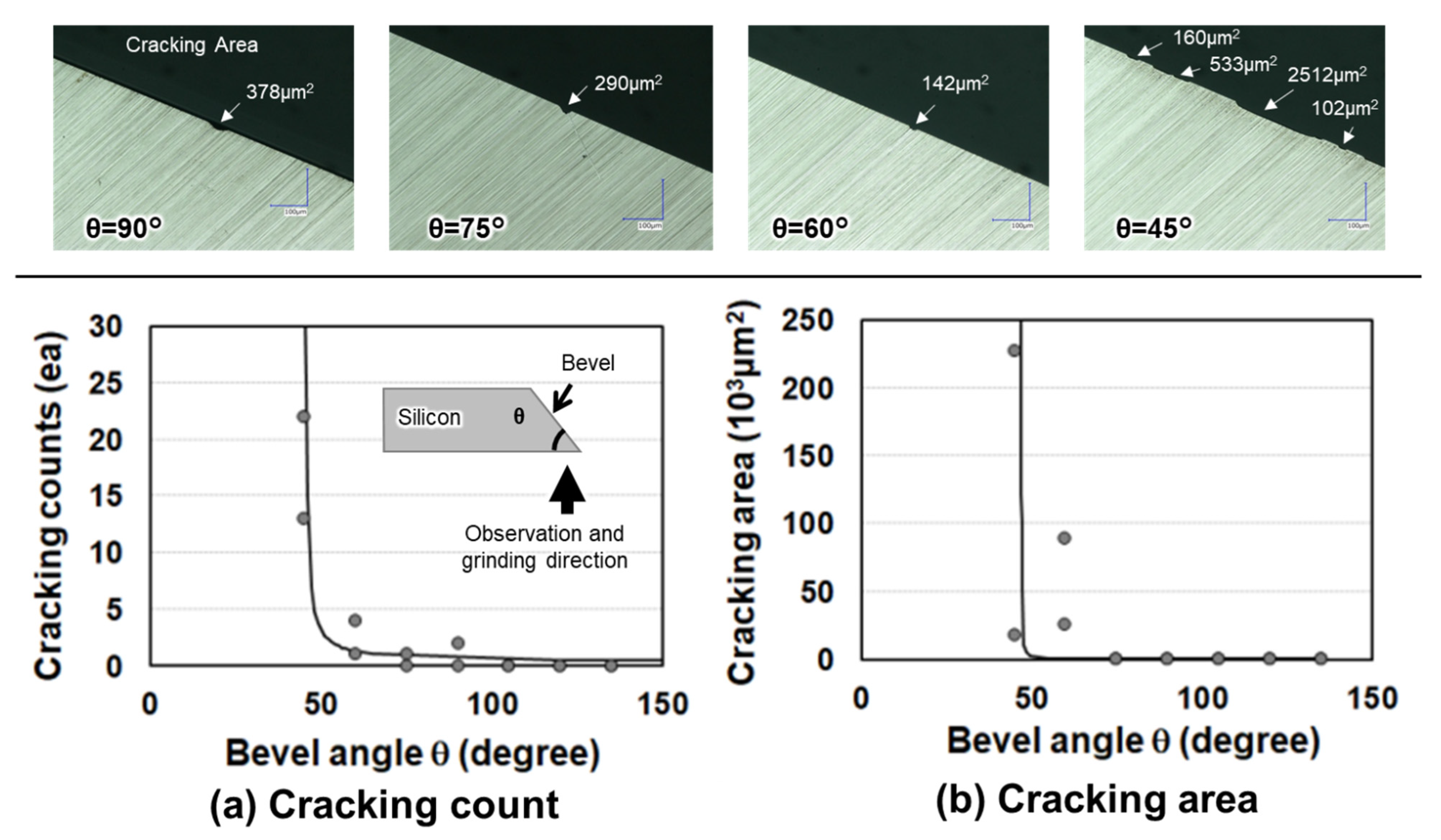
- Aoki, T.; Hirasawa, M.; Izunome, K.; Ohba, T. Development of Novel Bevel Profile for Wafer-level Stacking Technology. In Proceedings of the International Conference on Electronics Packaging (ICEP), Tokyo, Japan, 12–14 May 2021; pp. 123–124. [Google Scholar]
- Mills, M.E.; Townsend, P.; Castillo, D.; Martin, S.; Achen, A. Benzocyclobutene (DVS-BCB) polymer as an interlayer dielectric (ILD) material. Microelectron. Eng. 1997, 33, 327–334. [Google Scholar] [CrossRef]
- Araki, N.; Maetani, S.; Kim, Y.S.; Hirota, T.; Nakamura, T.; Ohba, T. Material Optimization of Permanent and Temporary Adhesives for Wafer-level Three-dimensional Integration. In Proceedings of the IEEE 69th Electronic Components and Technology Conference (ECTC), Orlando, FL, USA, 3–30 June 2020; pp. 56–61. [Google Scholar]
- Edelstein, D.; Heidenreich, J.; Goldblatt, R.; Cote, W.; Uzoh, C.; Lustig, N.; Roper, P.; McDevittt, T.; Motsifft, W.; Simon, A.; et al. Full Copper Wiring in a Sub-0.25 μm CMOS ULSI Technology. In Proceedings of the IEEE International Electron Devices Meeting (IEDM), Washington, DC, USA, 7–10 December 1997; pp. 773–776. [Google Scholar]
- Kitada, H.; Maeda, N.; Fujimoto, K.; Mizushima, Y.; Nakata, Y.; Nakamura, T.; Ohba, T. Diffusion Resistance of Low Temperature Chemical Vapor Deposition Dielectrics for Multiple Through Silicon Via on Bumpless Wafer-on-Wafer Technology. Jpn. J. Appl. Phys. 2011, 50, 05ED02. [Google Scholar] [CrossRef]
- Diehl, D.; Kitada, H.; Maeda, N.; Fujimoto, K.; Ramaswami, S.; Sirajuddin, K.; Yalamanchili, R.; Eaton, B.; Rajagopalan, N.; Ding, R.; et al. Formation of TSV for the Stacking of Advanced Logic Devices Utilizing Bumpless Wafer-on-Wafer Technology. Microelectron. Eng. 2011, 92, 3–8. [Google Scholar] [CrossRef]
- Kitada, H.; Maeda, N.; Fujimoto, K.; Suzuki, K.; Kawai, A.; Arai, K.; Suzuki, T.; Nakamura, T.; Ohba, T. Stress Sensitivity Analysis on TSV Structure of Wafer-on-a-Wafer (WOW) by the Finite Element Method (FEM). In Proceedings of the IEEE Proceedings of International Interconnect Technology Conference (IITC), Sapporo, Japan, 1–3 June 2009; pp. 107–109. [Google Scholar]
- Ohba, T. Wafer-Level Three-Dimensional Integration Using Bumpless Interconnects and Ultra-thinning. In 3D Integration in VLSI Circuits; Sakuma, K., Iniewski, K., Eds.; CRC Press: Boca Raton, FL, USA, 2018; pp. 86–210. [Google Scholar]
- Tsai, Y.-C.; Lee, C.-H.; Chang, H.-C.; Liu, J.-H.; Hu, H.-W.; Ito, H.; Kim, Y.S.; Ohba, T.; Chen, K.-N. Electrical Characteristics and Reliability of Wafer-on-Wafer (WOW) Bumpless Through-Silicon Via. IEEE Trans. Electron Device 2021, 68, 3520–3525. [Google Scholar] [CrossRef]
- Frank, T.; Moreau, S.; Chappaz, C.; Leduc, P.; Arnaud, L.; Thuaire, A.; Chery, E.; Lorut, F.; Anghel, L.; Poupon, G. Reliability of TSV interconnects: Electromigration, thermal cycling, and impact on above metal level dielectric. Microelectron. Rel. 2013, 53, 17–29. [Google Scholar] [CrossRef]
- Akamatsu, T.; Tadaki, S.; Yamazaki, K.; Kitada, H.; Sakuyama, S. Study of chip stacking process and electrical characteristic evaluation of Cu pillar joint between chips including TSV. In Proceedings of the IEEE Electronic Components and Technology Conference (ECTC), Las Vegas, NV, USA, 31 May–3 June 2016; pp. 1827–1833. [Google Scholar]
- Funaki, T.; Satake, Y.; Kobinata, K.; Hsiao, C.-C.; Matsuno, H.; Abe, S.; Kim, Y.S.; Ohba, T. Miniaturized 3D Functional Interposer using Bumpless Chip-on-Wafer (COW) Integration with Capacitors. In Proceedings of the IEEE Electronic Components and Technology Conference (ECTC), San Diego, CA, USA, 1 June–4 July 2021; pp. 185–190. [Google Scholar]
- Mizushima, Y.; Kitada, H.; Uchibori1, C.J.; Maeda, N.; Kodama, S.; Kim, Y.S.; Fujimoto, K.; Yoshimi, S.; Nakamura, T.; Ohba, T. Impacts of Thermo-Mechanical Stresses on Bumpless Chip in Stacked Wafer Structure. Jpn. J. Appl. Phys. 2013, 52, 05FE01. [Google Scholar] [CrossRef] [Green Version]
- Satake, Y.; Funaki, T.; Tabata, K.; Kobinata, K.; Kim, Y.S.; Ohba, T. Development of Functional Interposer Using Bumpless Chip-on-Wafer. In Proceedings of the International Conference on Solid State Devices and Materials (SSDM), Virtual Conference, 27–30 September 2020; pp. 119–120. [Google Scholar]
- Kim, Y.S.; Kodama, S.; Mizushima, Y.; Araki, N.; Hsiao, C.; Chang, H.; Lin, C.; Ohba, T. Optimization of Via Bottom Cleaning for Bumpless Interconnects and Wafer-On-Wafer (WOW) Integration. In Proceedings of the IEEE Electronic Components and Technology Conference (ECTC), San Diego, CA, USA, 29 May–1 June 2018; pp. 1962–1963. [Google Scholar]
- Mead, C.; Rem, M. Minimum Propagation Delays in VLSI. IEEE J. Solid-State Circuits 1982, 17, 773–775. [Google Scholar] [CrossRef]
- Kang, S.-M.; Leblebici, Y. CMOS Digital Integrated Circuits, 2nd ed.; McGraw-Hill: New York, NY, USA, 1999. [Google Scholar]
- Martin, K. Digital Integrated Circuit Design; Oxford University Press: Oxford, UK, 2000. [Google Scholar]
- Dennard, R.H. Field-Effect Transistor Memory. U.S. Patent 3,387,286, 4 June 1986. [Google Scholar]
- Masuoka, F. Semiconductor Memory Device. U.S. Patent 4,437,174, 13 March 1984. [Google Scholar]
- Masuoka, F.; Momodomi, M.; Iwata, Y.; Shirota, R. New Ultra High Density EPROM and Flash EEPROM with NAND Structure Cell. In Proceedings of the IEEE International Electron Devices Meeting (IEDM), Washington, DC, USA, 6–9 December 1987; pp. 552–555. [Google Scholar]
- Lee, D.U.; Kim, K.W.; Kim, H.; Kim, J.Y.; Park, Y.J.; Kim, J.H.; Kim, D.S.; Park, H.B.; Shin, J.W.; Cho, J.H.; et al. A 1.2V 8Gb 8-Channel 128GB/s High-Bandwidth Memory (HBM) Stacked DRAM with Effective Microbump I/O Test Methods Using 29nm Process and TSV. In Proceedings of the IEEE International Solid-State Circuits Conference (ISSCC), San Fransisco, CA, USA, 9–13 February 2014; pp. 432–433. [Google Scholar]
- Lee, J.C.; Kim, J.; Kim, K.W.; Ku, Y.J.; Kim, D.S.; Jeong, C.; Yun, T.S.; Kim, H.; Cho, H.S.; Kim, Y.O.; et al. A 1.2V 64Gb 8-Channel 256GB/s HBM DRAM with Peripheral-Base-Die Architecture and Small-Swing Technique on Heavy Load Interface. In Proceedings of the IEEE International Solid-State Circuits Conference (ISSCC), San Fransisco, CA, USA, 31 January–4 February 2016; pp. 318–319. [Google Scholar]
- Sohn, K.; Yun, W.-J.; Oh, R.; Oh, C.-S.; Seo, S.-Y.; Park, M.-S.; Shin, D.-H.; Jung, W.-C.; Shin, S.-H.; Ryu, J.-M.; et al. A 1.2V 20nm 307GB/s HBM DRAM with At-Speed Wafer-Level I/O Test Scheme and Adoptive Refresh Considering Temperature Distribution. In Proceedings of the IEEE International Solid-State Circuits Conference (ISSCC), San Fransisco, CA, USA, 31 January–4 February 2016; pp. 316–317. [Google Scholar]
- Cho, J.H.; Kim, J.; Lee, W.Y.; Lee, D.U.; Kim, T.K.; Park, H.B.; Jeong, C.; Park, M.-J.; Baek, S.G.; Choi, S.; et al. A 1.2V 64Gb 341GB/s HBM2 Stacked DRAM with Spiral Point-to-Point TSV Structure and Improved Bank Group Data Control. In Proceedings of the IEEE International Solid-State Circuits Conference (ISSCC), San Fransisco, CA, USA, 11–15 February 2018; pp. 208–209. [Google Scholar]
- Oh, C.-S.; Chun, K.C.; Byun, Y.-Y.; Kim, Y.-K.; Kim, S.-Y.; Ryu, Y.; Park, J.; Kim, S.; Cha, S.; Shin, D.; et al. A 1.1V 16GB 640GB/s HBM2E DRAM with a Data-Bus Window-Extension Technique and a Synergetic On-Die ECC Scheme. In Proceedings of the IEEE International Solid-State Circuits Conference (ISSCC), San Francisco, CA, USA, 16–20 February 2020; pp. 330–331. [Google Scholar]
- Lee, D.U.; Cho, H.S.; Kim, J.; Ku, Y.J.; Oh, S.; Kim, C.D.; Kim, H.W.; Lee, W.Y.; Kim, T.K.; Yun, T.S.; et al. A 128Gb 8-High 512GB/s HBM2E DRAM with a Pseudo Quarter Bank Structure, Power Dispersion and an Instruction-Based At-Speed PMBIST. In Proceedings of the IEEE International Solid-State Circuits Conference (ISSCC), San Francisco, CA, USA, 16–30 February 2020; pp. 334–335. [Google Scholar]
- Jun, H.; Cho, J.; Lee, K.; Son, H.-Y.; Kim, K.; Jin, H.; Kim, K. HBM (High Bnadwidth Memory) DRAM Technology and Architecture. In Proceedings of the 2017 IEEE International Memory Workshop (IMW), Monterey, CA, USA, 14–17 May 2017. [Google Scholar]
- Ndip, I.; Curran, B.; Löbbicke, K.; Guttowski, S.; Reichl, H.; Lang, K.-D.; Henke, H. High-Frequency Modeling of TSVs for 3-D Chip Integration and Silicon Interposers Considering Skin-Effect, Dielectric Quasi-TEM and Slow-Wave Modes. IEEE Trans. Compon. Packag. Manufacuturing Technol. 2011, 1, 1627–1642. [Google Scholar] [CrossRef]
- Weis, C.; Jung, M.; Naji, O.; When, N.; Santos, C.; Vivet, P.; Hansson, A. Thermal Aspects and high-Level Explorations of 3D stacked DRAMs. In Proceedings of the 2015 IEEE Computer Society Annual Symposium on VLSI, Montpellier, France, 8–10 July 2015; pp. 609–614. [Google Scholar]
- Ryoson, H.; Fujimoto, K.; Ohba, T. A Design Guide of Thermal Resistance down to 30% for 3D multi-stack devices. In Proceedings of the 2017 International Conference on Electronics Packaging (ICEP), Yamagata, Japan, 19–22 April 2017; pp. 522–525. [Google Scholar]
- Sakui, K.; Ohba, T. High Bandwidth Memory (HBM) and High Bandwidth NAND (HBN) with the Bumpless TSV Technology. In Proceedings of the IEEE 2019 International 3D Systems Integration Conference, Sendai, Japan, 8–10 October 2019. 3DIC2019.4005. [Google Scholar]
- Sakui, K.; Ohba, T. Sophisticated Architecture for High Bandwidth Memory (HBM) and High Bandwidth NAND (HBN) with the Bumpless TSV Technology. In Proceedings of the 29th Materials for Advanced Metallization Conference, Grenoble, France, 16–18 November 2020. [Google Scholar]
- Tanaka, H.; Kido, M.; Yahashi, K.; Oomura, M.; Katsumata, R.; Kito, M.; Fukuzumi, Y.; Sato, M.; Nagata, Y.; Matsuoka, Y.; et al. Bit Cost Scalable Technology with Punch and Plug Process for Ultra High Density Flash Memory. In Proceedings of the 2007 Symposium on VLSI Technology, Kyoto, Japan, 12–14 June 2007; pp. 14–15. [Google Scholar]
- Sakui, K. Semiconductor Memory Device and Memory System. U.S. Patent 6,594,169B2, 15 July 2003. [Google Scholar]
- Maleville, C.; Asper, B.; Poumeyrol, T.; Moricean, H.; Bruel, M.; Auberton-Herve, A.J.; Barge, T.; Metral, F. Silicon-on Insulator and Devices VII; Hemment, P.L.F., Cristoloveanu, S., Izumi, K., Houston, T., Wilson, S., Eds.; Electrochem. Soc.: Pennington, NJ, USA, 1996; p. 34. [Google Scholar]
- Kagawa, Y.; Fujii, N.; Aoyagi, K.; Kobayashi, Y.; Nishi, S.; Todaka, N.; Takeshita, S.; Taura, J.; Takahashi, H.; Nishimura, Y.; et al. Novel stacked CMOS image sensor with advanced Cu2Cu hybrid bonding. In Proceedings of the IEEE International Electron Devices Meeting (IEDM), San Francisco, CA, USA, 3–7 December 2016; pp. 208–2011. [Google Scholar] [CrossRef]
- Natarajan, S. A 32 nm logic technology featuring 2nd-generation high-k + metal-gate transistors, enhanced channel strain and 0.171 μm2 SRAM cell size in a 291Mb array. In Proceedings of the IEEE International Electron Devices Meeting (IEDM), San Francisco, CA, USA, 15–17 December 2008; pp. 941–943. [Google Scholar]
- Sugatani, S.; Chujo, N.; Sakui, K.; Ryoson, H.; Nakamura, T.; Ohba, T. Vertically Replaceable Memory Block Architecture for Stacked DRAM Systems by Wafer-on-Wafer (WOW) Technology. IEEE Trans. Electron Devices 2020, 67, 4606–4610. [Google Scholar] [CrossRef]
- Sugatani, S.; Chujo, N.; Sakui, K.; Ryoson, H.; Nakamura, T.; Ohba, T. Bumpless Build Cube (BBCube) using Wafer-on-Wafer (WOW) Technology with 3D-manner Redundancy Scheme. In Proceedings of the International Conference on Solid State Devices and Materials (SSDM), Virtual Conference, 27–30 September 2020. [Google Scholar]
- Jun, H.; Nam, S.; Jin, H.; Lee, J.-C.; Park, Y.J.; Lee, J.J. High-Bandwidth Memory (HBM) Test Challenges and Solutions. IEEE Des. Test 2017, 34, 16–25. [Google Scholar] [CrossRef]
- Toroflux Paradox: Making Things (Dis)appear with Math. Available online: https://www.youtube.com/watch?v=VK7XR-wlpAk (accessed on 29 December 2021).
- O’Connor, M.; Chatterjee, N.; Lee, D.; Wilson, J.; Agrawal, A.; Keckler, S.W.; Dally, W.J. Fine-Grained DRAM: Energy-Efficient DRAM for Extreme Bandwidth Systems. In Proceedings of the 50th Annual IEEE/ACM International Symposium on Microarchitecture (MICRO), Cambridge, MA, USA, 14–18 October 2017; pp. 41–54. [Google Scholar]
- Available online: https://www.youtube.com/watch?v=1r_tSjZCNzg (accessed on 29 December 2021). (In Japanese).
- Price, D.W.; Robinson, J.; Bhatti, N.; VonDenHoff, M.; Lim, A.; Rathert, R.J.; Sherman, K.; Sutherland, D.; Cappel, R.; Meenakshisundaram, G. Application of Inline Defect Part Average Testing (I-PAT) to Reduce Latent Reliability Defect Escapes. Available online: https://www.kla-tencor.com/documents/KLA_I-PAT_AEC_October_2018.pdf (accessed on 6 February 2020).
- Clark, R. Advanced Process Technologies Required for Future Scaling and Devices, Short Course 1. In Proceedings of the IEEE Symposium on VLSI Technology, Kyoto, Japan, 9–14 June 2019. [Google Scholar]
- Fatemeh, T.; Siavash, E.; Shujuan, W.; Kambiz, V. Analysis of Critical Thermal Issues in 3D Integrated Circuits. Int. J. Heat Mass Transf. 2016, 97, 337–352. [Google Scholar]
- Ankur, J.; Robert, J. Analytical and Numerical Modeling of Thermal Performance of Three-Dimensional Integrated Circuits. IEEE Trans. Compon. Packag. Technol. 2010, 33, 56–63. [Google Scholar]
- Gian, L.; Banit, A.; Navin, S.; Sheng-Chin, L.; Timothy, S.; Kaustav, B. A thermaly-Aware Performance Analysis of Vertically Integrated (3-D) Processor-Memory Hierarchy. In Proceedings of the Design Automation Conference (DAC), San Francisco, CA, USA, 24–28 July 2006; Available online: https://www.cs.ucsb.edu/~sherwood/pubs/DAC-3dmodel.pdf (accessed on 25 December 2021).
- Chatterjee, S.; Cho, M.; Rao, R.; Mukhopadhyay, S. Impact of Die-to-Die Thermal Coupling on the Electrical Characteristics of 3D Stacked SRAM Cache. In Proceedings of the 28th IEEE Semiconductor Thermal Measurement and Management Symposium (SEMI-THERM), San Jose, CA, USA, 18–22 March 2012. [Google Scholar]
- Matsumoto, K.; Ibaraki, S.; Sueoka, K.; Sakuma, K.; Kikuchi, H.; Orii, Y.; Yamada, F.; Fujihira, K.; Takamatsu, J.; Kondo, K. Thermal Design Guidelines for a Three-dimensional (3D) Chip Stack, Including Cooling Solutions. In Proceedings of the 29th IEEE Semiconductor Thermal Measurement and Management Symposium (SemiTherm 2013), San Jose, CA, USA, 17–21 March 2013. [Google Scholar]
- Ohba, T.; Nakamura, T. 3D stacked integration technologies: Overview and future prospects, Oyo Buturi. Jpn. Soc. Appl. Phys. 2020, 89, 75–81. (In Japanese) [Google Scholar]


| Permanent Adhesive on Adhesion Promoter | Adhesion Promoter | Temporary Adhesive | |
|---|---|---|---|
| Thickness | 0.5–5 μm | ~10 nm | 2–20 μm |
| Softening Temperature | around 50 °C | - | over 100 °C |
| Solidification | 135 ± 5 °C, 30 min and 170–195 °C, 30 min | 100–120 °C, 5 min | - |
| De-bonding | - | - | mechanical peeling at 80 kPa or over 200 °C |
| Cleaning Solvent | - | - | DTB-Cleaner |
| Modified Tape Peel Test of Stacked Wafers, After TCT 1000 Cycles | no delamination | - | - |
| 3DI w/Micro-Bumps | BBCube WOW | |||
|---|---|---|---|---|
| Gen1 | Gen2 | |||
| Thick. (μm) | Epoxy (1) | 19.5 | - | |
| Epoxy (2) | 6.0 | 1.5 | ||
| SiO2 (1) | 5.0 | 4.5 | ||
| SiO2 (2) | 1.5 | - | ||
| Si | 55.0 | 4.0 | ||
| Total | 87.0 | 10.0 | ||
| TSV dia. (μm) | 8.0 | 4.0 | 2.0 | |
| TSV pitch (μm) | 55.0 | 12.0 | 5.5 | |
| Relative Permittivity | Bulk Conductivity (Siemens/m) | |
|---|---|---|
| Copper | 1.0 | 5.8 × 10⁷ |
| Si | 11.9 | 10 |
| SiO2 | 4.0 | 0 |
| Solder | 1.0 | 7 × 10⁶ |
| Epoxy | 3.6 | 0 |
| TSV with Micro Bump 51.4 μm Pitch 25 μm Bump | Bumpless TSV 512 × 16 TSV 5 μm Gap | ||||||
|---|---|---|---|---|---|---|---|
| Components | Equivalent Thermal Conductivity (W/mK) | Thickness (μm) | Thermal Resistance (Kcm2/W) | Thickness (μm) | Thermal Resistance (Kcm2/W) | ||
| DRAM | Top Chip Rth1 | Si | 148 | 150 | 0.049 | 5 | 0.00034 |
| BEOL | 1.44 | 15 | 0.104 | - | - | ||
| 3.99 | - | - | 15 | 0.038 | |||
| Interconnection Micro Bump | 2.54 | 20 | 0.079 | - | - | ||
| Interconnection Bumpless | 2.56 | - | - | 5 | 0.02 | ||
| 2–8 Chip 7 Layers Rth2–8 | Si with TSV | 160.5 | 50 | 0.003 | 5 | 0.00031 | |
| BEOL | 1.44 | 15 | 0.104 | - | - | ||
| 3.99 | - | - | 15 | 0.038 | |||
| Interconnection Micro Bump | 2.54 | 20 | 0.079 | - | - | ||
| Interconnection Bumpless | 2.56 | - | - | 5 | 0.02 | ||
| Logic RthL | Si with TSV | 160.5 | 50 | 0.003 | 5 | 0.0003 | |
| Total Thermal Resistance | Rth1 + 7 × Rth2–8 + RthL | - | - | 1.54 | - | 0.46 | |
Publisher’s Note: MDPI stays neutral with regard to jurisdictional claims in published maps and institutional affiliations. |
© 2022 by the authors. Licensee MDPI, Basel, Switzerland. This article is an open access article distributed under the terms and conditions of the Creative Commons Attribution (CC BY) license (https://creativecommons.org/licenses/by/4.0/).
Share and Cite
Ohba, T.; Sakui, K.; Sugatani, S.; Ryoson, H.; Chujo, N. Review of Bumpless Build Cube (BBCube) Using Wafer-on-Wafer (WOW) and Chip-on-Wafer (COW) for Tera-Scale Three-Dimensional Integration (3DI). Electronics 2022, 11, 236. https://doi.org/10.3390/electronics11020236
Ohba T, Sakui K, Sugatani S, Ryoson H, Chujo N. Review of Bumpless Build Cube (BBCube) Using Wafer-on-Wafer (WOW) and Chip-on-Wafer (COW) for Tera-Scale Three-Dimensional Integration (3DI). Electronics. 2022; 11(2):236. https://doi.org/10.3390/electronics11020236
Chicago/Turabian StyleOhba, Takayuki, Koji Sakui, Shinji Sugatani, Hiroyuki Ryoson, and Norio Chujo. 2022. "Review of Bumpless Build Cube (BBCube) Using Wafer-on-Wafer (WOW) and Chip-on-Wafer (COW) for Tera-Scale Three-Dimensional Integration (3DI)" Electronics 11, no. 2: 236. https://doi.org/10.3390/electronics11020236