Article

A Procedure to Design Feasible Dual Band Matching Networks with Minimum Complexity

by
Alessandro DiCarlofelice
*,
Emidio DiGiampaolo
and
Piero Tognolatti
Dipartimento di Ingegneria Industriale e dell’Informazione e di Economia, University of L’Aquila, I-67100 L’Aquila, Italy
*
Author to whom correspondence should be addressed.
Electronics 2022, 11(21), 3569; https://doi.org/10.3390/electronics11213569
Submission received: 11 October 2022 / Revised: 27 October 2022 / Accepted: 31 October 2022 / Published: 1 November 2022
(This article belongs to the Special Issue Microwave Subsystems and Wireless Propagation)

Abstract

:
Many applications in communication systems require the development of dual band matching networks. A new method to design dual band matching networks was shown, which resorts to closed form equations based on transmission line theory, and has three particular characteristics: (i) it permits the minimum number of elements (two at most three) in the network; (ii) the topology of the network is not fixed but modular; and (iii) it is able to find multiple solutions within a predefined range of feasible characteristic impedances for the elements of the network. An extensive comparison with the results shown in the literature has been reported showing the improvements introduced by the proposed method. Numerical simulations and experimental results confirm the effectiveness of the method.

1. Introduction

There are a number of applications in communication systems that require working at multiple frequencies concurrently. In particular, there are applications such as radio frequency identification [1], harmonic radar [2], power amplifiers [3], and power dividers [4] that work at two frequencies, which require the development of dual band matching networks. There are also several works in the literature that face the problem of dual band matching networks, which can be grouped in methods for real loads and methods for complex loads. In the case of real loads, dual frequency transformers [5,6] perform the matching between a resistive load and a transmission line at the fundamental frequency and its first harmonic, [7] extends the method to two arbitrary frequencies while [8,9] solve that problem using the Chebyshev impedance transformer. A dual band stubbed T-junction was shown in [10], a multi-section transformer was proposed in [11] while a π-network was shown in [12]. Concerning methods for complex loads, [13] faced the problem in the case of complex conjugated loads while [14,15,16,17] addressed the complex impedance matching problem by resorting to an unequal two-section and a three-section impedance transformer, respectively. Nevertheless, the results shown have unfeasible characteristic impedances. A T-section impedance transformer was proposed in [18], while [19] used two-parts with two-section shunt stubs that permit the choice of the characteristic impedances of transmission lines. A π-network is frequently used in the simple form [20] and with additional shunt stubs [21], while a similar structure was recently proposed in [22,23] and in [24] that, instead, used a cascade of filters and phase shifters.
The mentioned methods were based on matching networks with predefined topologies, some of them adequately solve specific matching problems (i.e., for specific loads), while others, which have been proposed to be more general, provide, for particular loads, the characteristic impedance of the lines that cannot be realized. As an example, [25] showed that for a given set of complex load impedances, the T-section impedance transformer proposed in [18] calculated unfeasible characteristic impedances. To overcome this limit, it proposed increasing the complexity of the network by including an additional section called ‘load healing’. The increase in the number of elements of the network is often a redundant operation since it increases the degrees of freedom of a problem that only has four constraints. The availability of several degrees of freedom can be exploited to add constraints to the network system, for example, [19] imposed the choice of characteristic impedances using a network with four sections while [26], with a five-section network, imposed the rejection of a frequency besides the dual band matching.
It is clear that to solve the same kind of problem, methods involving very different network topologies with a different number of sections have been proposed, however, to the best of our knowledge, no one has proposed solving this type of problem by using a network with only two sections. From a mathematical point of view, two sections should be sufficient for this type of problem as they give four degrees of freedom (i.e., as many as the constraints). On the other hand, in an N-section network, the solution has to be found in a 2N dimensional space where the best solutions are hidden among many other suboptimal ones. It would be better to keep the dimension of the space the smallest possible in order to have easier solutions and simpler networks. It is evident that the equations to be solved are non-linear and transcendental, therefore four degrees of freedom may not be sufficient in particular situations, but for the same reason, for other loads, they could give a number of solutions greater than one.
We propose a new resolution method of the closed form equations of the dual band matching network problem for complex loads and any couple of frequencies that give solutions with the minimum number of sections (i.e., two at most three). We also show that most of the complex loads in the literature that have been matched with networks having more than three sections can be adequately matched with networks having only two sections. The method resorts only to transmission lines and is able to find multiple solutions within a predefined range of permissible characteristic impedances for the elements of the network.
The rest of this paper is organized as follows. Section 2 shows the closed form equations and the proposed resolution method, and Section 3 reports on the simulative and experimental results.

2. Matching Procedure

The topology of the network is modular and originates from the observation that two sections of a transmission line have four degrees of freedom, which would be sufficient to match a complex load to a transmission line with assigned characteristic impedance at two different frequencies. Nevertheless, there are particular loads for which that procedure is not able to exploit the four degrees of freedom adequately, so it is necessary to introduce a third line element.
The procedure consists of three steps. The first step determines the parameters of the main transmission line (( Z 1 , L 1 ) in Figure 1) connected to the load so that it brings the real part of the admittances (at the two frequencies) at its input port to coincide with the value of the desired matching admittance. For particular loads, the first step may not give a solution, in this case, a third line element (( Z 3 , L 3 ) in Figure 1) is introduced, which modifies the load impedance seen from the main transmission line and allows obtain a solution repeating the first step to be obtained. The last step adds a stub (( Z 2 , L 2 ) in Figure 1), which can be open or short, and it makes null the two susceptances (at the two frequencies) at the input port of the main transmission line. The procedure can be repeated recursively by changing some parameters, as shown in the next section, in order to tune the design parameters to the specification values. The method is intrinsically narrowband, making use of a few elements.
We consider a load Z L that has different impedances at two different frequencies. The envisaged matching network, shown in Figure 1, consists of two actual line elements with different characteristic impedance and length (blue colored) and a possible third line element (dashed contour) to be added in case the actual line elements are not sufficient to achieve the matching of the load to the characteristic impedance Z 0 .
Let Z 1 , Z 2 , and L 1 , L 2 be the characteristic impedances and the lengths, respectively, of the actual lines, these are unknowns to be determined to perform the matching.
Let Z L , a = R a + j X a and Z L , b = R b + j X b be the complex impedances of the load at frequency f a and f b , respectively, and υ = f b f a , υ > 1 ,   υ .
The reflection coefficient at the load is
Γ L , u = Z L , u Z 1 Z L , u + Z 1 ,  
that has magnitude Γ L , u and phase ϕ L , u where u a , b denotes one of the two frequencies [27].
The admittance at the input of the first line is
Y i n , 1 , u = 1 Z i n , 1 , u = 1 Z 1   1 Γ L , u e j 2 θ 1 , u ϕ L , u 1 + Γ L , u e j 2 θ 1 , u ϕ L , u
where Y i n , 1 , u and θ 1 , u is the electric length of the line (i.e., θ 1 , u = β 1 , u L 1 with β 1 , u the propagation constant at the frequency specified by index u ) [27].
The corresponding conductance is
G i n , 1 , u = 1 Z 1   1 Γ L , u 2 1 + Γ L , u 2 + 2 Γ L , u cos 2 θ 1 , u ϕ L , u
We infer that G i n , 1 , u = Y 0 = 1 Z 0 for each u a , b in order to have a couple of equations to determine the unknowns Z 1 and L 1 , which satisfy the first step of the matching procedure.
Equations are
1 Y 0 Z 1 Γ L , u 2 1 + Y 0 Z 1 2   Y 0 Z 1 Γ L , u cos 2 θ 1 , u ϕ L , u = 0
with u a , b .
Since Γ L , u is a function of Z 1 and θ 1 , u is a function of L 1 , these equations represent two curves (i.e., G i n , 1 , u = Y 0 ) , over the plane ( Z 1 , L 1 ); they may intersect at some points that are solutions to the system (4). From the first equation, we find
θ 1 , a = 1 2 ϕ L , a   ± cos 1 1 Y 0 Z 1 Γ L , a 2 1 + Y 0 Z 1 2   Y 0 Z 1 Γ L , a
that depends only on Z 1 and has to undergo the constraints
1 Y 0 Z 1 Γ L , a 2 1 + Y 0 Z 1 2   Y 0 Z 1 Γ L , a 1
and
θ 1 , a > 0
being representative of a physical line in the interval of Z 1 that we were interested in considering. In practice, Z 1 has to span over an interval of values that permits the practical feasibility of the line.
Since θ 1 , b = υ   θ 1 , a (assuming the line not dispersive), we can exploit the second equation of (4) to have
1 Y 0 Z 1 Γ L , b 2 1 + Y 0 Z 1 2   Y 0 Z 1 Γ L , b cos 2 υ θ 1 , a ϕ L , b = 0
that permits us to find the values of Z 1 solutions to the system (4) after including (5) in (8). This equation can be solved numerically by imposing constraints (6) and (7).
In general, there are four solutions to system (4) since (8) gives two solutions for each solution of (5) but may be cases of Z L for which no solution is available from (8). In this case, we introduce a further line element in order to obtain a solution. This is described and discussed in Section 2.1.
Once Z 1 and L 1 have been obtained, we determine Z 2 and L 2 by dimensioning a suitable stub that makes null the imaginary parts of Z i n , 2 , u . We considered both open and short circuit stub cases.
Let B i n , 1 , u be the imaginary part of Y i n , 1 , u ; in the case of an open circuit stub, we have to solve the system
Y 2 tan θ 2 , u + B i n , 1 , u = 0
which gives
tan υ θ 2 , a tan θ 2 , a = B i n , 1 , b B i n , 1 , a
and
Y 2 = B i n , 1 , a tan θ 2 , a
In the case of a short circuit stub, the solution is given by
tan θ 2 , a tan υ   θ 2 , a = B i n , 1 , b B i n , 1 , a
and
Y 2 = B i n , 1 , a tan θ 2 , a
Equations (10)–(13) give, in general, more solutions, but some of them may have Y 2 < 0 and are discarded.
Nevertheless, there are cases where
1 υ < B i n , 1 , b B i n , 1 , a < υ
where (11) and (13) do not have a solution.
Since the ratio B i n , 1 , b / B i n , 1 , a depends on the solution of (4), which in general has more than one solution, it is possible to find a particular solution of (4) that does not satisfy (14). In the case this is not possible, we introduced a third element in the matching network, as shown in the next subsection.

2.1. Third Line Elements

If the network made with two transmission line elements did not allow the matching, we introduced a third line element, as shown in Figure 1. This element can be placed in front of the load as a stub (open or short) (Figure 1a) or alternatively in series to connect the load to the ground (Figure 1b). The choice of the topology of that third element is arbitrary and alternative (i.e., if a choice does not lead to a satisfactory matching network, we can change the topology). Since we did not have any constraint to impose on the additional transmission line, we arbitrarily chose the characteristic impedance Z 3 and optimized the length L 3 in order to have satisfactory values of Z 1   2 and L 1   2 for the practical feasibility of the corresponding transmission lines.
The algorithm first calculates the electrical length θ 3 , a (i.e., at frequency f a ) that makes null the imaginary part of the impedance of the combination of that third element with the load at frequency f b . Let B L , b be the susceptance of the load at frequency f b and χ a tuning parameter to be varied arbitrarily, so we have three different results for the three alternative lines:
θ 3 , a = 1 υ tan 1 Z 3   ( B L , b χ
in the case of an open circuit stub;
θ 3 , a = 1 υ tan 1 1 Z 3   ( B L , b χ )
in the case of a short circuit stub; and
θ 3 , a = 1 υ tan 1 X L , b χ Z 3
in the case of a transmission line connecting the load to the ground.
Once Z 3 and L 3 have been determined, the algorithm restarts from (1), calculating the reflection coefficient Γ L , u and repeats the procedure. After a solution is obtained, θ 3 , a can be tuned repeating cyclically the procedure by varying Z 3 and χ in order to achieve the values of Z 1 , Z 2 and L 1 , L 2 as close as possible the specification values.
In general, the above described procedure provides more solutions that permit for the matching of the load using transmission lines with characteristic impedance inside an assigned interval.

3. Numerical Results and Experimental

The proposed procedure was validated numerically and experimentally. For the assigned values of the load at two specific frequencies, the procedure searched the possible matching networks under the constraint that the characteristic impedance of the lines was inside the interval 10 ÷ 125   Ω . Extensive numerical analysis was performed by means of an ad-hoc made program written in MATLAB [28], checking the behavior of the found matching networks for a large number of loads. The check was based on the analysis of the found solutions by means of Cadence AWR-DE [29] to verify that the reflection coefficient ( S 11 ) at the input port of the network had two matching deeps at the assigned frequencies. It has been found that most loads can be matched with only two line elements (i.e., Z 1 and Z 2 ) while the third element is necessary mainly when the load at the two frequencies is nearby the open circuit point of the Smith chart.
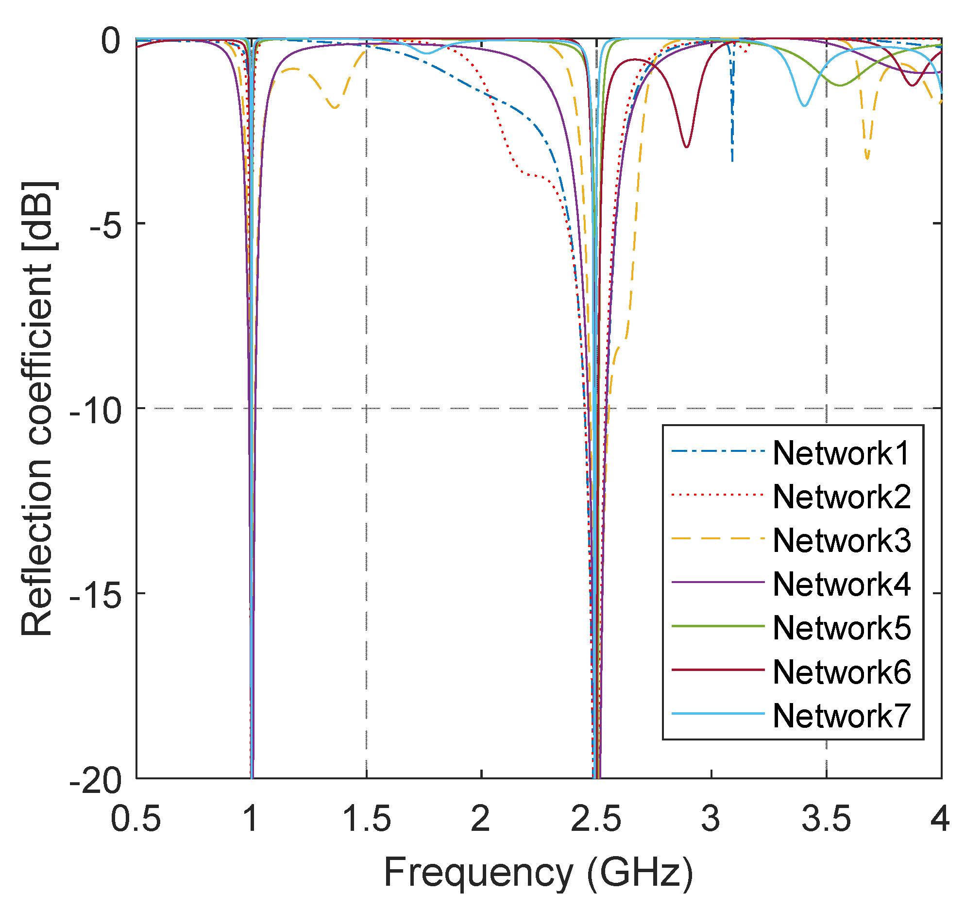
Table 1 reports some examples of matching results: the first column shows the complex impedance of the load at the two frequencies (in GHz) shown in column 2, the other columns show the characteristic impedance and the electric length (in degrees) @ f a of the elements of the matching network. We observed that multiple solutions were possible, some cases required three elements in the matching network, and in any case, the characteristic impedance of the lines was inside the predefined interval. Considering, as an example, the first case shown in Table 1 (i.e., Z L , a = 52 j 456   Ω   @ 1 GHz , Z L , b = 28 j 180   Ω   @ 2.5 GHz ), the proposed procedure found seven different matching networks able to match that load; the graphs of the reflection coefficient obtained with the numerical check are shown in Figure 2. Some solutions were very narrow band and the reflection coefficient was flat outside the band while others instead had a bandwidth that was a little bit larger but showed a ripple of the reflection coefficient outside the matching band.
The loads in the first column of Table 1 that have the symbol of reference were taken from the literature. All of them, in the corresponding papers, were matched with networks having a number of sections greater than or equal to three. With this method, we propose that they are matched with only two sections except for one, which requires three; moreover, it was observed that there were multiple solutions.
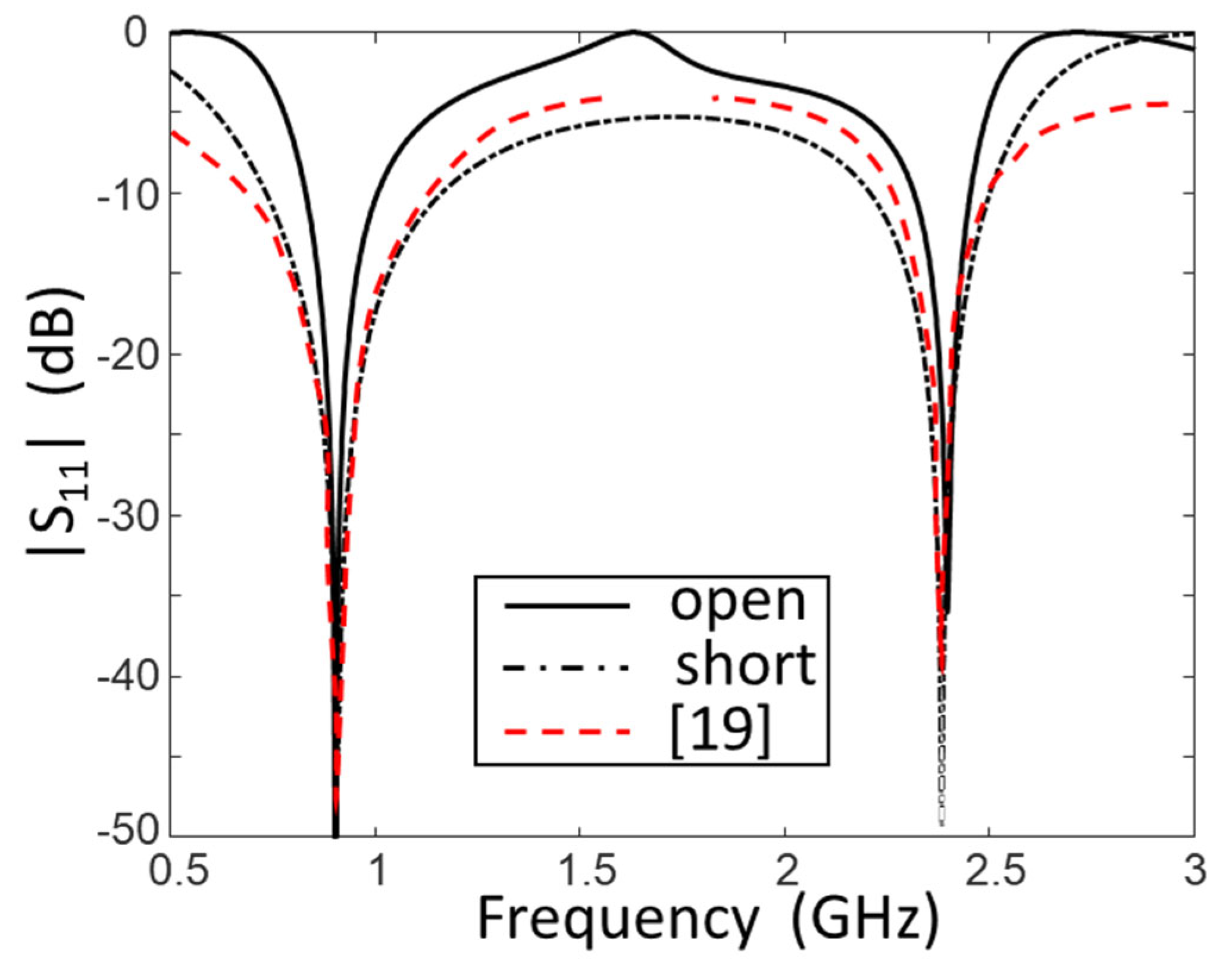
In order to check the effectiveness of the matching with two sections with respect to that obtained in the literature with several sections, we show in Figure 3 and Figure 4 the comparison between the reflection coefficients of two cases realized in [19,20]. The matching bandwidths at 10   d B in Figure 3 (black line) were 15 %   @   f a and 5 %   @   f b in the case of open stub while they were 40 %   @   f a and 11 %   @   f b in the case of the stub in short. In Figure 4, instead, the matching bandwidths were 6 %   @   f a and 4 %   @   f b . It is evident that the results obtained with the two-section networks were as adequate as those shown in the literature.
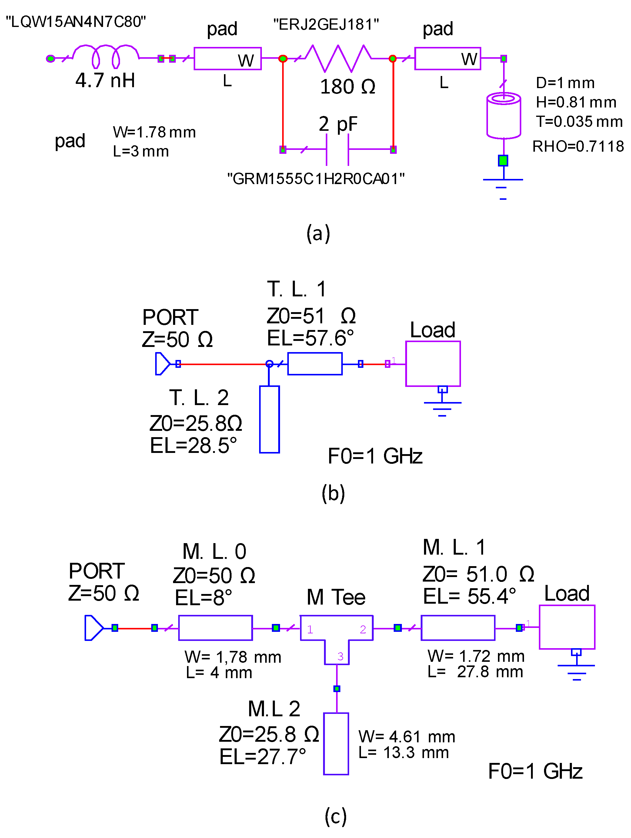
The experimental validation consisted of the realization and measurement of a matching network corresponding to the third case in Table 1. The load was made with a lumped circuit with 180   Ω resistance in parallel to a 2   pF capacitance with a 4.7   nH inductance in series, as shown in Figure 5a, where the names of the used components are also shown. The model of the load accounts for pads and via-hole that are used to realize the circuit so that the input impedance of the overall load circuit is Z L , a = 22.5 j 22   Ω   @   1   GHz and Z L , b = 5 + j   66.5   Ω   @   2.4   GHz .
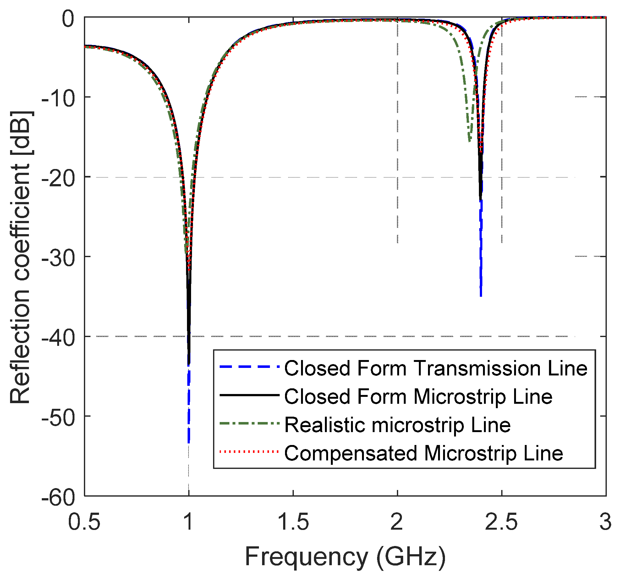
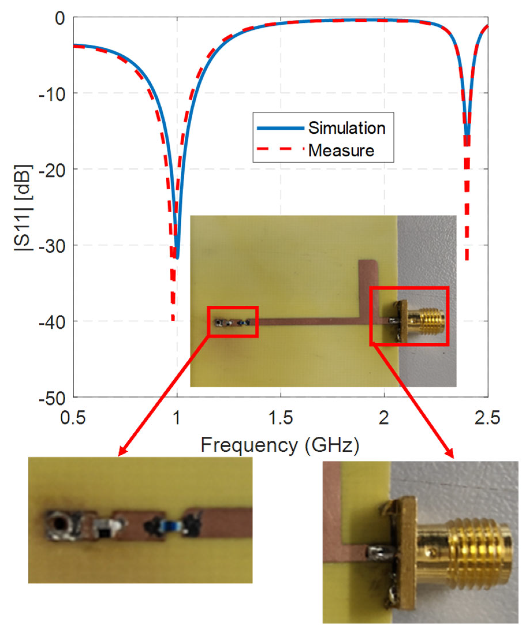
At least eight two-section matching networks were possible for that load and we realized the first one shown in Table 1 (i.e., Z 1 = 51   Ω ,   θ 1 , a = 57.6 °   and   Z 2 = 25.8   Ω ,   θ 2 , a = 28.5 ° ) that had an open stub. The overall circuit was realized with microstrip lines over the R4003C substrate having a thickness of 0.81 mm, ϵ r = 3.55 ,   tan δ = 0.0027 . Evidently, the calculated parameters of the matching transmission lines do not take into account the parasitic effects that arise in a real microstrip line circuit because of the discontinuities such as the end effect of the open stub and the reactances introduced by the T-junction. A simulative comparison of the reflection coefficients of different models of the matching network is shown in Figure 6. The models are based on the schematics shown in Figure 5b,c, they concern: (i) closed form solutions (Figure 5b) and (ii) a realistic microstrip line (Figure 5c). Closed form solutions make use of the found parameters in a lossless theoretical transmission line model and in a microstrip model that takes into account the losses of the substrate. As shown in Figure 6, the corresponding reflection coefficients differed mainly for the depth of the matching hollows. In the realistic microstrip line model, we introduced the T-junction element and the end effect on the stub, preserving the lengths and the impedances of the lines. In this case, a shift toward lower frequency was observed @   f b (dash-dotted green line in Figure 6). Nevertheless, a simple compensation [30] that slightly reduces the lengths of the lines (obtained values shown in Figure 5c) permits the circuit to be exactly matched (dotted black line in Figure 6). The compensated microstrip line circuit was realized and measured, and the obtained reflection coefficient, shown in Figure 7, had good agreement with the simulation result. The matching bandwidths were 20 %   @   f a and 1.6 %   @   f b .
The prototype was realized using a milling and drilling machine T-Tech quick circuit 5000 while measurements were performed using a Vector Network Analyzer Anritsu MS46122B, calibrated with 5001 sample points inside the bandwidth of 0.5 GHz–2.5 GHz.

4. Conclusions

A new resolution method of the closed form equations of the dual band matching network problem for complex loads and any couple of frequencies was shown. This was able to provide multiple solutions to the matching problem with the minimum number of sections (i.e., two at most three). All provided solutions are feasible and we have shown that it allows for the realization of simple networks in many practical cases. A detailed comparison with the results shown in the literature has been reported, showing the improvements introduced by the proposed method. A specific prototype was realized and measured, confirming the theoretical achievement. Its major limitation is the lack of the control of the width of the matching band since it is intrinsically narrowband. Overcoming this limit may be addressed in future works.

Author Contributions

Conceptualization, A.D.; Methodology, A.D. and E.D.; Software, A.D. and E.D.; Validation, A.D.; Writing—original draft preparation, A.D.; Writing—review and editing, E.D. and P.T.; Supervision, E.D. and P.T. All authors have read and agreed to the published version of the manuscript.

Funding

This research received no external funding.

Data Availability Statement

Not applicable.

Conflicts of Interest

The authors declare no conflict of interest.

References

  1. Paredes, F.; Gonzalez, G.; Bonache, J.; Martín, F. Dual-Band Impedance-Matching Networks Based on Split-Ring Resonators for Applications in RF Identification (RFID). IEEE Trans. Microw. Theory Tech. 2010, 58, 1159–1166. [Google Scholar] [CrossRef]
  2. Gu, X.; Srinaga, N.N.; Guo, L.; Hemour, S.; Wu, K. Diplexer-Based Fully Passive Harmonic Transponder for Sub-6-GHz 5G-Compatible IoT Applications. IEEE Trans. Microw. Theory Tech. 2019, 67, 1675–1687. [Google Scholar] [CrossRef]
  3. Meng, X.; Yu, C.; Wu, Y.; Liu, Y. Design of Dual-Band High Efficiency Power Amplifiers Based on Compact Broadband Matching Networks. IEEE Microw. Wirel. Compon. Lett. 2018, 28, 162–164. [Google Scholar] [CrossRef]
  4. Wu, L.; Sun, Z.; Yilmaz, H.; Berroth, M. A dual-frequency wilkinson power divider. IEEE Trans. 2006, 54, 278–284. [Google Scholar] [CrossRef]
  5. Chow, Y.L.; Wan, K.L. A transformer of one-third wavelength in two sections-for a frequency and its first harmonic. IEEE Microw. Wireless Compon. Lett. 2002, 12, 22–23. [Google Scholar] [CrossRef]
  6. Monzon, C. Analytical derivation of a two-section impedance transformer for a frequency and it first harmonic. IEEE Microw. Wireless Compon. Lett. 2002, 12, 381–382. [Google Scholar] [CrossRef]
  7. Monzon, C. A small dual-frequency transformer in two sections. IEEE Trans. Microw. Theory Tech. 2003, 51, 1157–1161. [Google Scholar] [CrossRef]
  8. Orfanidis, S.J. A two-section dual-band Chebyshev impedance transformer. IEEE Microw. Wirel. Compon. Lett. 2003, 13, 382–384. [Google Scholar] [CrossRef]
  9. Castaldi, G.; Fiumara, V.; Gallina, I. An exact synthesis method for dual-band Chebyshev impedance transformers. Prog. Electromagn. Res. 2008, 86, 305–319. [Google Scholar] [CrossRef] [Green Version]
  10. Park, M.; Lee, B. Dual-band design of sing-stub impedance matching networks with application to dual-band stubbed T-junctions. Microw. Opt. Technol. Lett. 2010, 52, 1359–1362. [Google Scholar] [CrossRef]
  11. Liu, L.; Geng, J.; Liu, F.; Fan, H.; Liang, X.; Wang, W.; Jin, R. A Novel Analytical Method for Multi-Frequency Transmission Line Transformer. IEEE Microw. Wirel. Compon. Lett. 2016, 26, 556–558. [Google Scholar] [CrossRef]
  12. Wu, Y.; Liu, Y.; Li, S. A compact Pi-structure dual band transformer. Prog. Electromagn. Res. 2008, 88, 121–134. [Google Scholar] [CrossRef] [Green Version]
  13. Colantonio, P.; Giannini, F.; Scucchia, L. A new approach to design matching networks with distributed elements. In Proceedings of the MIKON’04, Poland, Warsaw, 17–19 May 2004; Volume 3, pp. 811–814. [Google Scholar]
  14. Wu, Y.; Liu, Y.; Li, S.; Yu, C.; Liu, X. A generalized dual-frequency transformer for two arbitrary complex frequency-dependent impedances. IEEE Microw. Wirel. Compon. Lett. 2009, 19, 792–794. [Google Scholar] [CrossRef]
  15. Wu, Y.L.; Liu, Y.A.; Li, S.L. A dual-frequency transformer for complex impedances with two unequal sections. IEEE Microw. Wirel. Compon. Lett. 2009, 19, 77–79. [Google Scholar] [CrossRef]
  16. Liu, X.; Liu, Y.A.; Li, S.L.; Wu, F.; Wu, Y.L. A three-section dual band transformer for frequency-dependent complex load impedance. IEEE Microw. Wirel. Compon. Lett. 2009, 19, 611–613. [Google Scholar] [CrossRef]
  17. Sinha, R. Comments on A Three-Section Dual-Band Transformer for Frequency-Dependent Complex Load Impedance. IEEE Microw. Wirel. Compon. Lett. 2019, 29, 783–785. [Google Scholar] [CrossRef]
  18. Nikravan, M.A.; Atlasbaf, Z. T-section dual-band impedance transformer for frequency-dependent complex loads. Electron. Lett. 2011, 47, 551–553. [Google Scholar] [CrossRef]
  19. Chuang, M.-L. Dual-band impedance transformer using two-section shunt stubs. IEEE Trans. Microw. Theory Tech. 2010, 58, 1257–1263. [Google Scholar] [CrossRef]
  20. Manoochehri, O.; Asoodeh, A.; Forooraghi, K. Pi-model dual-band impedance transformer for unequal complex impedance loads. IEEE Microw. Wirel. Compon. Lett. 2015, 25, 238–240. [Google Scholar]
  21. Zheng, X.; Liu, Y.; Li, S.; Yu, C.; Wang, Z.; Li, J. A Dual-Band Impedance Transformer Using Pi-Section Structure for Frequency-Dependent Complex Loads. Prog. Electromagn. Res. C 2012, 32, 11–26. [Google Scholar]
  22. Saxena, A.; Banerjee, D.; Gupta, R.; Hashmi, M. Design of πStructure Dual-Band Matching Network With Unequal Susceptance Cancellation Stubs. In Proceedings of the 2018 IEEE MTT-S International Microwave and RF Conference (IMaRC), Kolkata, India, 28–30 November 2018; pp. 1–3. [Google Scholar]
  23. Saxena, A.; Banerjee, D.; Hashmi, M.; Auyenur, M. A Dual-Band Impedance Transfomer for Matching Frequency Dependent Complex Source and Load Impedances. In Proceedings of the 2019 15th Conference on Ph.D Research in Microelectronics and Electronics (PRIME), Lausanne, Switzerland, 15–18 July 2019; pp. 173–176. [Google Scholar]
  24. Yazdani, F.; Mansour, R.R. Realization of Dual-Band Matching Networks Using Cascaded Filters. In Proceedings of the 2020 50th European Microwave Conference (EuMC), Utrecht, The Netherlands, 12–14 January 2021; pp. 727–730. [Google Scholar]
  25. Maktoomi, M.A.; Hashmi, M.S.; Ghannouchi, F.M. Improving Load Range of Dual-Band Impedance Matching Networks Using Load-Healing Concept. IEEE Trans. Circuits Syst. II Express Briefs 2017, 64, 126–130. [Google Scholar] [CrossRef]
  26. Chuang, M.-L.; Wu, M.-T. General Dual-Band Impedance Transformer With a Selectable Transmission Zero. IEEE Trans. Compon. Packag. Manuf. Technol. 2016, 6, 1113–1119. [Google Scholar] [CrossRef]
  27. Pozar, D.M. Microwave Engineering; John Wiley & Sons: Hoboken, NJ, USA, 2009. [Google Scholar]
  28. Matlab. Available online: https://www.mathworks.com/ (accessed on 27 October 2022).
  29. AWR Software. Available online: https://www.awr.com/ (accessed on 27 October 2022).
  30. Gupta, K.C.; Garg, R.; Bahl, I.J.; Barthia, P. Microstrip Lines and Slotlines, 2nd ed.; Artech House: Norwood, MA, USA, 1996. [Google Scholar]
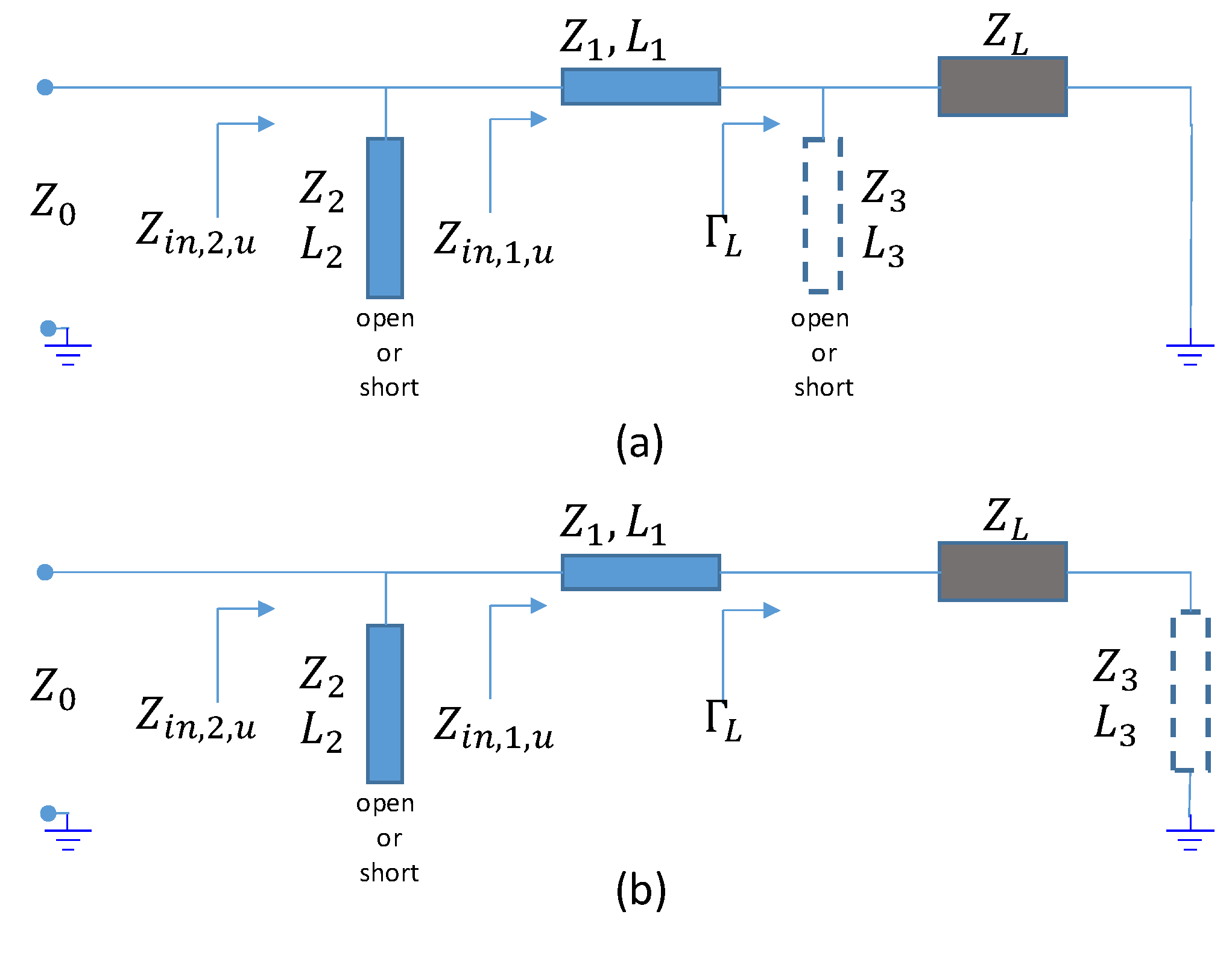
Figure 1. Circuit diagram of the matching network. Z L is the load to be matched at two frequencies f a and f b ; Z 1   2 and L 1   2 are parameters of transmission lines to be determined to match Z L to Z 0 . Z 3 and L 3 parameters of a possible additional transmission line: it can be placed in front of the load as a stub (open or short) (a) or alternatively in series (b).
Electronics 11 03569 g001
Figure 2. Reflection coefficient of the matching networks corresponding to the first case in Table 1 (i.e. Z L , a = 52 j 456   Ω   @ 1   G H z , Z L , b = 28 j 180   Ω   @ 2.5   G H z ). The numbering of the legend corresponds to the presenting order in Table 1.
Electronics 11 03569 g002
Figure 3. Comparison between the reflection coefficient obtained with two-section networks (continuous black line) and that reported in the literature (dashed red line) for the case [19] in Table 1.
Electronics 11 03569 g003
Figure 4. Comparison between the reflection coefficient obtained with two-section networks (continuous and dash-dotted black lines) and those reported in the literature (dashed red line) for the case [20] in Table 1.
Electronics 11 03569 g004
Figure 5. Schematics of the realized circuit with relevant parameters: (a) circuit of the load; (b) transmission line (T.L.) model of the matching network; (c) compensated microstrip line (M.L.) model of the matching network.
Electronics 11 03569 g005
Figure 6. Comparison of simulative results for four circuit models of the experimental matching circuit.
Electronics 11 03569 g006
Figure 7. Simulative reflection coefficient of the compensated microstrip line matching network compared to the measurement of the realized circuit. The inset shows a picture of the realized circuit while the enlargements show details of the circuit (left) and connector (right).
Electronics 11 03569 g007
Table 1. Some examples of the matching results 1.
Z L , a
Z L , b
f a
f b
Z 1   / θ 1 ,   a Z 2   / θ 2 ,   a Z 3   / θ 3 ,   a
52 − j456
28 − j180
1.0
2.5
43.8/90.975.7/86 (o)70/27.5 (l)
22.5/76.7 (o)
124.7/67.313.2/139 (o)
34/24 (s)
35.1/48.218.6/99.6 (o)70/53.1 (o)
56.7/43.811.7/160.8 (s)
21.5/112.712.2/99.9 (o)70/27.7 (s)
22 − j 403
16 − j 386
0.867
0.920
15.7/74.240.8 (o)/94.240/80 (l)
34.2/89.7110.5 (s)/176.7
22.5 − j22
5 + j66.5
1.0
2.4
51/57.625.8/28.5 (o)n.n.
72.2/146.6 (s)
57.6/50.344/43.1 (o)
91.2/152.8 (s)
25/115.849/40.2 (o)
105.8/151.3 (s)
22.2/125.744/34.6 (o)
105.3/148.8 (s)
[14] a 400 + j30
400 + j30
1
2
80/122.440/119 (o)50/58.5 (s)
13.5/59 (s)
[14] b 400 + j40
400 + j40
1
3.5
120/80.832/160 (o)n.n.
[19] a 200 + j60
250 + j100
2.4
5.8
100/10936/102 (s)n.n.
[19] b 100 − j 35.4
150 − j6.4
0.9
2.4
44/45.237.7/51.2 (s)n.n.
27.9/149.2 (o)
[20] 10 − j66.3
10 − j44.2
2.4
3.6
78.3/28.714.4/142.3 (o)n.n.
[22] a 100 + j80
150 + j100
1
1.8
33.4/68.527.3/130.5 (o)
11/65.9 (s)
n.n.
[22] b 50 + j80
60 + j 120
1
1.8
15/66.411/131.9 (o)n.n.
[22] c 100 + j0
120 + j0
1
2
44/5240/54.7 (s)n.n.
20.4/160.1 (o)
68.6/103.659.6/101.9 (s)
[25] a 92.8 − j15.8
78.8 − j21.5
1
2
57.5/50.864.1/58.5 (s)n.n.
57.6/111.164.4/121.5 (s)
[25] b 10.3 − j11.9
11.1 + j24.4
1
2
21.8/85.620.5/66.4 (s)n.n.
65.5/125.7 (o)
[25] c 155.9 − j27
130.4 − j54.8
1
2.5
84.8/95.554.2/108 (s)n.n.
37.4/102.6 (s)
[25] d 86.5 + j13.4
90.1 + j21.4
1.5
2.5
29.6/138.836.2/134 (s)n.n.
87.5/66.8 (o)
61.8/77.964.3/69.6 (s)
[26] 101 − j35.4
101 − j15.2
0.9
2.1
59.6/47.562.4/52.2 (s)n.n.
27.8/160.9 (o)
62.5/101.331.7/109.3 (s)
1 Units: impedance: ohm; frequency: GHz; electric length: degrees: Symbols in the table: (s) short circuit stub; (o) open circuit stub; (l) line to ground; n.n. not necessary.
Publisher’s Note: MDPI stays neutral with regard to jurisdictional claims in published maps and institutional affiliations.