Article

Timing Analysis and Optimization Method with Interdependent Flip-Flop Timing Model for Near-Threshold Design

National ASIC System Engineering Center, Southeast University, Nanjing 210096, China
*
Author to whom correspondence should be addressed.
These authors contributed equally to this work.
Electronics 2022, 11(22), 3670; https://doi.org/10.3390/electronics11223670
Submission received: 18 October 2022 / Revised: 8 November 2022 / Accepted: 8 November 2022 / Published: 10 November 2022

Abstract

:
Near-threshold Voltage (NTV) design is receiving wide attention due to remarkable energy efficiency improvement at the cost of performance degradation. The interdependency between the setup–hold time and clock-to-q delay of flip-flops has been exploited in the Super-threshold Voltage (STV) domain to improve circuit performance but faces the severe challenge of nonlinear relationship and wider effective coverage in the NTV region, which prevents the application of interdependent flip-flop model for timing analysis and optimization for NTV design. In this paper, a novel interdependent flip-flop timing model is proposed by Artificial Neural Network (ANN) to predict the clock-to-q delay with training data generated by SPICE simulation in a restricted hexagonal area of the two-dimensional setup-hold time space. By integrating the proposed model into Static Timing Analysis (STA) flow, a novel iterative optimization method is proposed to improve performance for NVT circuits based on a Genetic Algorithm (GA). The proposed timing analysis and optimization method were validated under Semiconductor Manufacturing International Corporation (SMIC) 40 nm process at the voltage of 0.6 V with the International Symposium on Circuits and Systems (ISCAS)’89 benchmark circuits. Experimental results demonstrate that the ANN-based interdependent timing model for flip-flop achieves considerable accurate prediction with the Mean Absolute Relative Error (MARE) of less than 0.69%. The minimum clock periods for ISCAS’89 benchmark circuits are reduced by 1.70~6.28% compared to traditional STA results without any setup and hold violations and hardware cost, which achieves at most 6.7% performance improvement for NTV design.

1. Introduction

With the development of the microelectronics craft technique, modern IC design attaches great importance to the Performance, Power, and Area (PPA) of chips [1,2,3]. The technique of reducing the supply voltage to near-threshold voltage (NTV) region is receiving more attention in recent years due to remarkable energy efficiency improvement but suffers from severe challenges of performance variation for Static Timing Analysis (STA) [4,5,6]. In order to guarantee timing closure, an extra timing margin has to be added to compensate for pessimistic timing estimation at the cost of unneglectable area and power overhead [7,8,9]. In recent decades, the interdependency between the timing constraints of sequential logic cells has been exploited, modeled, and utilized in STA to prevent timing violations without any hardware cost [10,11]. However, compared with the super-threshold voltage (STV) region, the accurate modeling for the interdependency of setup time, hold time, and clock-to-q delay becomes much more complicated in NTV region because of nonlinear relationship and wider effective coverage, which limits its application for timing analysis and optimization in NTV circuit design.
Plenty of prior works have been devoted to interdependent timing modeling for sequential cells and related circuit optimization. The work in [12] introduced a simulation-based approach that exploits the interdependent model by operating SPICE simulation for setup and hold time. In spite of considerable accuracy, this method may suffer from high simulation costs, especially when the simulation range is broadened in NTV region. In [13], an analytical model was proposed based on circuit-level parameters to capture the setup–hold-time interdependency in a conventional master-slave flip-flop, which is too complicated to be integrated into STA. The approaches in [14,15,16] used a nonlinear function to depict the clock-to-q delay surface. However, the iteration-based method in [14] cannot guarantee to converge in a given number of iterations, while the model in [15,16] was not accurate enough. A piecewise linear model was proposed in [17] and introduced in [18] to characterize the relationship between clock-to-q delay and setup–hold time, in which a three-dimensional clock-to-q delay surface was approximately characterized as spliced small polygons. Owing to the learning ability to exploit complex relations with training data, artificial neural network (ANN) models were employed in [19,20] to characterize the timing interdependency for flip-flops, which achieved a trade-off between accuracy and simulation cost but were not applied for circuit optimization.
In spite of prior works, most of them focus on the interdependent timing model in STV region, where empirical fitting methods or linear approximation were utilized to capture the interdependency between setup–hold time and clock-to-q delay for sequential cells but will suffer from either the loss of accuracy or higher simulation cost in NTV region. The work in [19] characterized the interdependent timing constraints for flip-flops in the NTV region but lacks the application for timing analysis and optimization in NTV circuit design.
In this paper, a timing analysis and optimization framework was established for NTV circuit design by leveraging the interdependency between the setup–hold time and clock-to-q delay for flip-flops to improve circuit performance without any additional area and power cost, which is beneficial to the reduction of unnecessary circuit area and power consumption compared with traditional approach during fixing timing violations. Our contributions are summarized as follows:
  • In order to cope with the nonlinear relation and wide effective coverage of interdependency between the setup–hold time and clock-to-q delay for flip-flops in the NTV domain, the interdependent clock-to-q delay of the flip-flop is predicted by the ANN model, whose training data are generated by SPICE simulation in a restricted hexagonal area in the two-dimensional setup-hold time space, leading to high prediction accuracy and low simulation cost.
  • By integrating the ANN-based interdependent timing model into STA flow, an iterative circuit optimization method is proposed to minimize the clock period without any timing violations by balancing the timing slacks among iteratively selected paths, where Genetic Algorithm (GA) is employed to find the optimal setup time and hold time for each flip-flop in the selected paths.
The rest of the paper is organized as follows. Section 2 introduces the background of STA and timing interdependency for flip-flop. Section 3 proposes an ANN-based model to predict the interdependent clock-to-q delay for the flip-flop, which is utilized for the proposed iterative circuit optimization method in Section 4. The experimental results are shown in Section 5 and Section 6 concludes the whole work.

2. Background

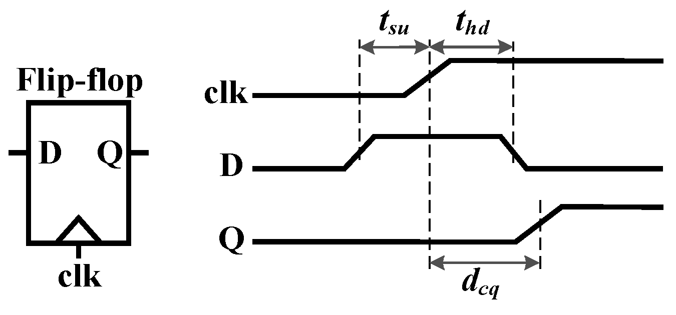
2.1. Traditional Timing Model for Flip-Flop

In traditional STA, the timing model for flip-flop is characterized by its setup time, hold time, and clock-to-q delay denoted as tsu, thd, and dcq, respectively, in Figure 1. To ensure the input data latched correctly, the input signal is supposed to maintain a stable state for the time at least tsu before the active clock edge (clk) and at least thd after the active clock edge, respectively. In this condition, the signal delay from the active clock edge to the output of the flip-flop (Q) is deemed constant and represented by dcq, but if the required time of either tsu or thd is not met, the flip-flop will not work correctly, and a timing violation will be reported.
The traditional way to measure setup time is to monitor the increase in clock-to-q delay during moving the switch of the input signal close to the active clock edge compared with the minimum clock-to-q delay when the switch of input signal is far away from the active clock edge by simulation. When the clock-to-q delay reaches a predefined value, e.g., 110% of the minimum delay, the setup time is defined as the distance between the signal switch and the active clock edge. The hold time is defined in a similar way while moving the switch of the input signal after the active clock edge close to it. Moreover, the clock-to-q delay is defined by this predefined delay, e.g., 110% of the minimum delay.
By taking the circuit path between FFi and FFj in Figure 2 as an example, the setup and hold timing check can be performed to verify whether timing constraints are met with positive setup and hold slacks, as shown in (1) and (2).
Setup   slack = T + t c l k j t c l k i d c q i d max i , j t s u j 0
Hold   slack = t c l k i + d c q i + d min i , j t c l k j t h d j 0
where d m a x i , j ( d m i n i , j ) is the maximum (minimum) delay of the data path between flip-flop i and j, d c q i is the clock-to-q delay of flip-flop i, t s u j ( t h d j ) is the setup (hold) time of flip-flop j, t c l k i ( t c l k j ) is the launch (capture) clock path delay, and T is the clock period. Setup slack and hold slack represent the timing margin of circuit optimization. If the setup slack of a timing path is positive, the clock period can be reduced for, at most, the slack value without setup timing violation for this path. As a result, the circuit performance can be improved, but if the setup (hold) slack is negative, a setup (hold) violation will happen, and circuit optimization should be carried out by gate sizing or buffer insertion to fix it at the cost of iteration time and area/power effort.

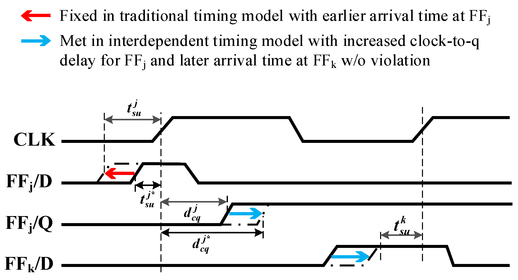
2.2. Interdependent Timing Model for Flip-Flop

It has been pointed out by prior works that the traditional model oversimplifies the timing characteristics of flip-flop since it leaves out the interdependency between clock-to-q delay and setup–hold time [17], which could be illustrated in Figure 3. As can be seen in Figure 3, the two-dimensional region where the setup time and hold time are large enough is defined as the stable region, where the clock-to-q delay of the flip-flop keeps constant to be the minimum, a.k.a 100% clock-to-q delay. When decreasing the setup time and/or the hold time, the flip-flop starts to leave the stable region, and the clock-to-q delay begins to increase gradually. Finally, the flip-flop fails to work when the setup time and hold time are too short, and the clock-to-q delay increases to be larger than a boundary value, which is defined as the metastable region.
Due to the interdependency among the setup time, hold time, and clock-to-q delay, it could be concluded that the traditional timing model induces a pessimism of timing behavior of flip-flop by considering that the setup time and hold time should both be large enough to keep the clock-to-q delay larger be equivalent as 110%. However, in practice, the setup time could be relatively short, with a large hold time to achieve 110% clock-to-q delay or vice versa. Moreover, both the setup time and the hold time could even be shorter when a relatively larger clock-to-q delay than 110% is allowed.
The interdependency among the setup time, hold time, and clock-to-q delay could be utilized to fix timing violations with the traditional flip-flop timing model. For the circuit with cascaded timing paths, as shown in Figure 2, the circuit optimization procedure with an interdependent timing model could be demonstrated in Figure 4. Assume the setup timing path between FFi and FFj is considered to be violated while the setup timing check for the path between FFj and FFk is met with sufficient timing margin under the traditional timing model. With the traditional flip-flop timing model, the setup violation for the timing path between FFi and FFj is induced due to the setup slack between the arrival time of input data and the clock edge of FFj, t s u j , is less than the setup time t s u j , which should be fixed by gate sizing or buffer insertion to shorten the data path delay between FFi and FFj. However, with the consideration of the interdependency between the setup time and clock-to-q delay, the input data to FFj could still be transmitted with a relatively small t s u j at the cost of a larger clock-to-q delay, d c q j , than traditional d c q j , which will delay the arrival time of input data for FFk and so decrease the setup slack for the path between FFj and FFk, but will not lead to timing violation. In this way, the negative timing slack for the path between FFi and FFj is compensated by the timing margin from the path between FFj and FFk owing to the timing dependency of flip-flop without any hardware overhead from gate sizing or buffer insertion.
Unfortunately, compared with the STV region, NTV design poses a severe challenge to the interdependent timing model for flip-flops. Figure 5 compares the setup-hold time pair curve in the NTV region with the STV region by simulation results under the 40 nm process. In contrast to the approximately linear relationship in the STV region in Figure 5a, the setup–hold time pair curve is significantly nonlinear in the NTV region in Figure 5b, which induces difficulty for accurate modeling with empirical fitting parameters or linear approximation. In addition, it is shown in Figure 5 that the effective coverage of setup time and hold time in the NTV region is over 5.4 and 6.7 times that in the STV region, which may lead to a much higher simulation cost for characterization.

3. Interdependent Timing Model Characterized by ANN

In this section, the effective coverage for setup time and hold time in the NTV domain is determined by SPICE simulation and restricted in a hexagonal region in the two-dimensional setup–hold time space. With the carefully selected features, the interdependent clock-to-q delay is predicted by an ANN model, which is integrated into the conventional STA flow to update the timing slack by taking the interdependency of the timing constraint of flip-flops into account.

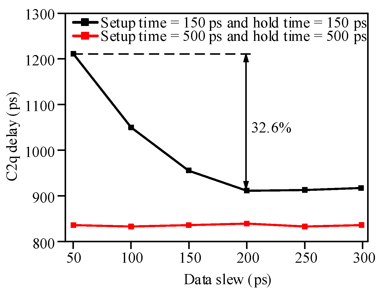
3.1. Selection of Effective Coverage

Due to the much wider effective coverage for setup time and hold time of flip-flops, as demonstrated in Figure 5, the simulation range should be carefully selected to cover the dominant area for the interdependent timing constraint for flip-flops under specific clock transition, data transition, and load capacitance. Noticing that the flip-flop remains in a stable region when the switch of data signal is far away before and after the active clock edge while falls into a metastable region when the switch of data signal is quite close to the active clock edge, the effective region of SPICE simulation is restricted in a hexagonal region in the two-dimensional setup-hold time space by trimming the stable and metastable regions.
The procedure to define the hexagonal simulation region is illustrated in Figure 6. Firstly, by keeping the setup and hold time large enough, the flip-flop operates in the stable region where the minimum clock-to-q delay, a.k.a 100% clock-to-q delay, could be measured by SPICE simulation, as shown at point A in Figure 6. Then by decreasing the setup time with a binary search and keeping the hold time fixed, points B and C are defined where the flip-flop leaves the stable region and enters the metastable region, respectively, which are indicated by the increase in clock-to-q delay and the operation failure. In addition, by decreasing the hold time with a binary search and keeping the setup time fixed, point D could be determined based on point B, where the clock-to-q delay begins to increase, and point E could be determined by points C and D accordingly. Besides point D and E, another two vertexes of the hexagonal simulation range, point H and I, could be determined similarly based on point F and G. For the other two vertexes, point J is determined by point D and I, and point K is determined by point H and E, respectively.
It can be found that in the hexagonal simulation range, both the range of setup time and hold time are restricted to ensure the clock-to-q delay varies between the minimum to the maximum when the flip-flop operates correctly.

3.2. ANN-Based Prediction Model

In order to capture the interdependency between clock-to-q delay and setup–hold time, an ANN-based model is established to predict the clock-to-q delay with carefully selected features. Besides the setup time and hold time, the clock transition and output load capacitance are selected as features since they are used as indexes in the traditional timing library. Although the data transition is not involved, its influence on clock-to-q delay should be considered when the setup time and hold time get close to the metastable region in the NTV domain. Figure 7 shows the influence of the data transition on clock-to-q delay under the condition that clock transition is 500 ps and load capacitance is 20 fF at 0.6 V, 25 °C, TT corner under 40 nm process. Although the data transition has little effect on clock-to-q delay when both setup time and hold time are larger enough, it causes an increase of 32.6% in clock-to-q delay when it changes from 200 to 50 ps under the condition that both setup time and hold time are 150 ps, which is close to the metastable region. Therefore, it is reasonable to take data transition into account for the interdependent timing model.
With the selected features, the structure of ANN is illustrated in Figure 8. The input layer accepts the features including setup time (tsu), hold time (thd), data transition (sd), clock transition (sck), and output load capacitance (cld), while the output layer produces the clock-to-q delay (dcq) as the function of input features shown in (3).
dcq = f(tsu, thd, sd, sck, cld)
The number of hidden layers and the number of neurons for each layer will be validated and compared in terms of prediction accuracy.
In this work, the trained ANN model is integrated into the traditional STA flow to take the timing interdependency of the flip-flop into account, as shown in Figure 9. In traditional STA flow, the netlist, timing library, and constraint file are imported by STA tool, e.g., PrimeTime (PT), to report the setup–hold timing slack by the delays of launch clock path, capture clock path, data path as well as clock-to-q delay and setup–hold time. With the integrated ANN-based model, the interdependent clock-to-q delay is predicted by the applicable setup–hold time within the effective coverage and the data transition, clock transition, and output load capacitance of flip-flops reported by PT so that the timing slack is updated by the interdependent timing model for flip-flops instead of the interpolation value with the lookup tables in timing library.

4. Timing Optimization Method with Interdependent Timing Model

In this section, an iterative timing optimization method is raised with the integrated ANN-based interdependent timing model for the flip-flop, where GA is adapted to find the optimal setup and hold time for each flip-flop in the iterative selected critical paths.

4.1. Formulation of Timing Optimization Problem

The timing optimization problem for a design can be formulated as the problem to minimize the clock period (T) by ensuring that all setup and hold time checks are met for all available paths between flip-flops as indicated by (1) and (2), where the interdependent clock-to-q delay for flip-flops is predicted by (3), as expressed in the following.
minimize T
subject to (1,2), ∀path and (3), ∀flip-flop
Note that by integrating the interdependent model into STA flow, timing optimization is carried out by compensating the setup–hold time in the path with negative slack with the clock-to-q delay in the path with abundant positive timing slack or vice versa, as illustrated in Figure 4, which balances the timing slacks for concatenated circuit paths so as to achieve a decreased clock period compared with traditional STA.

4.2. Iterative Optimization Method

When performing timing optimization with the consideration of the timing interdependency of flip-flops, the solution space grows exponentially with the scale of the circuit due to the correlation between the concatenated circuit paths, which poses a great challenge to the optimization process in terms of runtime. To cope with this problem, we propose an iterative optimization method implemented with GA to improve circuit performance and fix timing violations, where the critical paths related to a certain number of flip-flops are iteratively chosen for timing optimization to trade-off between performance improvement and runtime.
The proposed iterative optimization method is illustrated in Figure 10. Firstly, STA is performed to report timing slack for each circuit path between flip-flops with the traditional flip-flop timing model. By sorting paths ascendingly according to their slacks, a group of top critical paths is selected to make sure that a certain number of flip-flops, namely N, operate as launch flip-flops or capture flip-flops in these paths. Considering that concatenated circuit paths may be involved by the setup–hold time and clock-to-q delay of these N flip-flips, all circuit paths related to these flip-flops are selected as the candidates of timing optimization in this iteration by employing GA to balance the timing slacks between concatenated paths and fix timing violations, which will be described in Algorithm 1 later. After this, with the optimal setup–hold time by GA and the corresponding clock-to-q delay predicted by the ANN model, the circuit performance is compared with that before this iteration in terms of the minimum clock period. If any performance improvement is observed in recent iterations, the timing optimization would be performed iteratively for another group of paths related to the N flip-flips in the top critical paths. Otherwise, the optimization stops.
Algorithm 1. GA optimization
01.
procedure GA
02.
  Initialize T to ensure setup slack in (1) are positive (∀ path collected)
03.
  Initialize timing information (∀ path, ∀ flip-flop collected)
04.
  Initialize hexagons for setup–hold time range (∀ flip-flop collected)
05.
  Initialize individual number of the population
06.
  Initialize parameters for selection, crossover, and mutation
07.
  Initialize C to determine the convergence condition
08.
  cv ← 0
09.
  epoch ← 0
10.
  population[epoch] ← Initialize population(individual number)
11.
  while True do
12.
    for each individual k in population[epoch] do
13.
      for all collected flip-flop j do
14.
       (tsu(k,j), thd(k,j)) ← corresponding variables in the individual
15.
       dcq(k,j) ← ANN-based interdependent model in (3)
16.
      end for
17.
      hw ← False
18.
      for all collected timing path i do
19.
       if hold slack in (2) is negative and worse than previous then
20.
        hw ← True
21.
        break 
22.
       end if 
23.
       end for 
24.
       if hw is True then
25.
         dismiss this individual
26.
         continue 
27.
       end if 
28.
       for all collected timing path i do
29.
         Tki ← minimum T to make setup slack in (1) positive
30.
       end for 
31.
       Tk ← maximum Tki, ∀ path collected
32.
      end for 
33.
      T’ ← minimum Tk, ∀ individual
34.
      best individual of population[epoch] ← the individual with T’
35.
      ΔTT-T’
36.
      ifΔT ≤ 0 then
37.
        cvcv + 1
38.
      else then
39.
        cv ← 0
40.
        TT’
41.
      end if
42.
      if cv > C then
43.
        return T, best individual of population[epoch]
44.
      end if
45.
      parents ← select(population[epoch])
46.
      epoch ← epoch + 1
47.
      population[epoch] ← crossover(parents)
48.
     population[epoch] ← mutate(population[epoch])
49.
  end while
50.
end procedure
The GA procedure for timing optimization in each iteration can be described in Algorithm 1. During the initialization, with the initial minimum clock period, T, which ensures that no setup violations are induced with traditional STA in line 2, the timing information, including the data path delay and timing slacks for the selected group of critical paths, is imported in line 3 as well as the data transition, clock transition and load capacitance for each flip-flop, which are used to initialize the hexagons to restrict the effective coverage of setup and hold time for each collected flip-flop in line 4. Moreover, the individual number and the parameters for selection, crossover, and mutation parameters for GA are initialized in lines 5 and 6. The convergence condition is defined for the GA process when the minimum clock period cannot decrease during the previous C epochs in line 7, and cv is initialized in line 8 to count the epochs for convergence. The population of GA is initialized for the first epoch in lines 9 and 10, which is evaluated during iterations until convergence. In each epoch of the population, the individual is comprised of variables, including setup–hold time for each collected flip-flop and the optimization target, the minimum clock period T, as the criterion for fitness. A smaller T represents a higher fitness of the individual and vice versa. According to the setup and hold time, tsu(k, j) and thd(k, j), from the k-th individual for the j-th flip-flop in line 14, the corresponding clock-to-q delay, dcq(k, j), could be predicted by the ANN-based interdependent model in line 15. Then the hold timing check is performed from line 17 to line 27. If the hold slacks for any of the selected timing paths are negative and worse than the previous iteration, the Boolean flag hw is set as true, and the individual is dismissed at once. Otherwise, the setup timing checks are performed for all selected timing paths to avoid any violations with a minimum clock period Tk as the criterion for individual fitness of the k-th epoch from line 28 to line 31. The individual with the minimum clock period T’ is recognized as the best one of the population for the current epoch in lines 33 and 34. For the previous C epochs, if the minimum clock period does not decrease any more, the population is terminated, and the best individual is considered to be found, as shown from line 35 to line 44. Otherwise, the population continues by updating the parameters for the next epoch from line 45 to line 48.

5. Experimental Results and Discussion

5.1. Experimental Setup

As illustrated in Figure 11, this work is established on a computer equipped with Intel CORE i5 Processor and 8 GB memory. The dataset to train the ANN model is generated from the SPICE simulation. The ANN model is trained and tested in MATLAB. The proposed timing optimization method with an ANN-based interdependent timing model for flip-flop was established by Python, where the GA was implemented using the toolbox Geatpy [21]. Several circuits from International Symposium on Circuits and Systems (ISCAS)’89 benchmark were utilized to validate the proposed method under the process of Semiconductor Manufacturing International Corporation (SMIC) 40 nm with the timing library in the NTV domain. For GA, the roulette-wheel selection, two-point crossover, and binary mutation are applied. The crossover probability was set as 0.9, the mutation probability was set as 0.15, and the number of individuals was set as 100.

5.2. Prediction Accuracy Validation of ANN-Based Interdependent Model

We employed several ANN architectures to explore the trade-off between accuracy and complexity. In Table 1, the data array in the Architecture column denotes the architecture of ANN, where the first and the last array elements are for the input and output layer, respectively, while the middle are for hidden layers. With the increase in the number of hidden layers and the related nodes, the complexity of ANN increases accordingly in terms of the number of edges, and the corresponding prediction error is evaluated in terms of Mean Absolute Relative Error (MARE) for clock-to-q delay with rise and fall input data switch of flip-flop, respectively. It can be seen that when the complexity of ANN increases, the prediction accuracy is improved and less than 1% with over 480 edges in the architecture of (5,20,15,5,1), which is adopted as the ANN-based interdependent flip-flop timing model for the proposed iterative timing optimization method due to considerable good balance between accuracy and complexity.

5.3. Performance Improvement Validation of Iterative Timing Optimization Method

To demonstrate the performance improvement with the proposed iterative timing optimization method, the benchmark circuits were utilized to reduce the minimum clock period by avoiding setup and hold violations, and the optimization results were compared with traditional STA and the previous work in [15], as illustrated in Table 2. It is shown that with the proposed timing optimization method, the minimum clock period is reduced by 1.70~6.28%, which indicates at most 6.7% performance improvement in terms of working frequency increase without any hardware cost. Compared with the approach in [15], which uses a nonlinear function to depict the interdependent clock-to-q delay surface, the proposed method achieves an additional 1.37% reduction of the minimum clock period by average.
It should be noted that owing to the iterative optimization for the candidates from the top critical paths, the proposed optimization method shows a good capability to avoid dramatic runtime increases for large-scale circuits, which is advantageous for the application of large-scale industrial design. As demonstrated in Figure 12, each benchmark circuit is dotted to represent the relation between the number of total timing paths and the optimization runtime. With the fitted trend as a red dashed line, it can be concluded that the runtime of the proposed method increases approximately logarithmically with the scale of the circuit.
In addition, the proposed timing optimization method benefits from fast convergence speed, as demonstrated in Figure 13, where the circuit s38583 is taken as an example to show the minimum clock period during iteration compared with the traditional STA method. It can be seen that although the minimum clock period is larger than the traditional STA result with initial individuals in GA, it decreases dramatically during propagation. With 22% of the total runtime before convergence, over 52% of the minimum clock period reduction is achieved.

6. Conclusions

In this work, an interdependent flip-flop timing model characterized by ANN is proposed and integrated into STA flow for NTV design. Based on it, an iterative optimization method is proposed to improve circuit performance without any additional hardware cost with GA. Experimental results show that the ANN-based interdependent clock-to-q prediction model demonstrates high accuracy of less than 0.69% MARE and appropriate complexity, and the iterative optimization method avoids dramatic runtime increase for a large-scale circuit with at most 6.7% performance improvement.

Author Contributions

P.C., Y.Q., and H.J. organized this work. Y.Q., P.C., and H.J. performed the modeling, simulation, and experiment work. The manuscript was written by Y.Q. and P.C. and edited by P.C. All authors have read and agreed to the published version of the manuscript.

Funding

This work was supported in part by the National Key Research and Development Program of China (Grant No. 2019YFB2205004), in part by the National Natural Science Foundation of China under Grant (62174031), in part by the Jiangsu Natural Science Foundation (Grant No. BK20201233), and in part by the SEU-SMIT EDA Joint Laboratory Project.

Conflicts of Interest

The authors declare no conflict of interest.

References

  1. Zhang, G.L.; Li, B.; Shi, Y.; Hu, J.; Schlichtmann, U. EffiTest2: Efficient Delay Test and Prediction for Post-Silicon Clock Skew Configuration Under Process Variations in IEEE Transactions on Computer-Aided Design of Integrated Circuits and Systems. IEEE Trans. Comput. Des. Integr. Circuits Syst. 2019, 38, 705–718. [Google Scholar] [CrossRef]
  2. Agni, S.K.B.; Jayagowri, R. Gate Matching Algorithm for Early False Path Detection in Statistical Static Timing Analysis. In Proceedings of the 2022 IEEE International Conference on Signal Processing, Informatics, Communication and Energy Systems (SPICES), Trivandrum, India, 10–12 March 2022; pp. 543–548. [Google Scholar] [CrossRef]
  3. Saurab, B.; Chavan, A.P. Design and Optimization of Timing Errors on Swapping of Threshold Voltage. In Proceedings of the 2021 IEEE Mysore Sub Section International Conference (MysuruCon), Hassan, India, 24–25 October 2021; pp. 687–691. [Google Scholar] [CrossRef]
  4. Kaul, H.; Anders, M.; Hsu, S.; Agarwal, A.; Krishnamurthy, R.; Borkar, S. Near-threshold voltage (NTV) design: Opportunities and challenges. In Proceedings of the 49th Annual Design Automation Conference (DAC ‘12), San Francisco, CA, USA, 3 June 2012; Association for Computing Machinery: New York, NY, USA, 2012; pp. 1153–1158. [Google Scholar] [CrossRef]
  5. Gautschi, M.; Schiavone, P.D.; Traber, A.; Loi, I.; Pullini, A.; Rossi, D.; Flamand, E.; Gurkaynak, F.K.; Benini, L. Near-Threshold RISC-V Core with DSP Extensions for Scalable IoT Endpoint Devices in IEEE Transactions on Very Large Scale Integration (VLSI) Systems. IEEE Trans. Very Large Scale Integr. (VLSI) Syst. 2017, 25, 2700–2713. [Google Scholar] [CrossRef] [Green Version]
  6. Heo, J.; Jeong, K.; Choi, J.Y.; Kim, T.; Choi, K. Hardware Performance Monitoring Methodology at Near-Threshold Computing and Advanced Technology Nodes: From Design to Postsilicon in IEEE Transactions on Computer-Aided Design of Integrated Circuits and Systems. IEEE Trans. Comput. Des. Integr. Circuits Syst. 2022, 41, 1929–1942. [Google Scholar] [CrossRef]
  7. Keller, S.; Harris, D.M.; Martin, A.J. A Compact Transregional Model for Digital CMOS Circuits Operating Near Threshold. IEEE Trans. Very Large Scale Integr. (VLSI) Syst. 2014, 22, 2041–2053. [Google Scholar] [CrossRef]
  8. Shiomi, J.; Ishihara, T.; Onodera, H. Microarchitectural-level statistical timing models for near-threshold circuit design. In Proceedings of the 20th Asia and South Pacific Design Automation Conference, Tokyo, Japan, 19–22 January 2015; pp. 87–93. [Google Scholar] [CrossRef]
  9. Golanbari, M.S.; Kiamehr, S.; Tahoori, M.B. Hold-time violation analysis and fixing in near-threshold region. In Proceedings of the 26th International Workshop on Power and Timing Modeling, Optimization and Simulation (PATMOS), Bremen, Germany, 21–23 September 2016; pp. 50–55. [Google Scholar] [CrossRef]
  10. Kanng, A.B.; Lee, H. Timing margin recovery with flexible flip-flop timing model. In Proceedings of the fifteenth International Symposium on Quality Electronic Design, Santa Clara, CA, USA, 3–5 March 2014; pp. 496–503. [Google Scholar] [CrossRef]
  11. Yang, Y.; Tam, K.H.; Jiang, I.H. Criticality-dependency-aware timing characterization and analysis. In Proceedings of the 52nd Annual Design Automation Conference (DAC ‘15), San Francisco, CA, USA, 7–11 June 2015; Association for Computing Machinery: San Francisco, CA, USA, 2015. [Google Scholar] [CrossRef]
  12. Saurabh, S.; Shah, H.; Singh, S. Timing Closure Problem: Review of Challenges at Advanced Process Nodes and Solutions. IETE Tech. Rev. 2019, 36, 580–593. [Google Scholar] [CrossRef]
  13. Balef, H.A.; Jiao, H.; de Gyvez, J.P.; Goossens, K. An analytical model for interdependent setup/hold-time characterization of flip-flops. In Proceedings of the 2017 18th International Symposium on Quality Electronic Design (ISQED), Santa Clara, CA, USA, 14–15 March 2017; pp. 209–214. [Google Scholar] [CrossRef]
  14. Chen, N.; Li, B.; Schlichtmann, U. Iterative timing analysis based on nonlinear and interdependent flipflop modelling. IET Circuits Devices Syst. 2012, 6, 330–337. [Google Scholar] [CrossRef]
  15. Heo, J.; Kim, T. Timing Analysis and Optimization Based on Flexible Flip-Flop Timing Model. In Proceedings of the 2016 IEEE Computer Society Annual Symposium on VLSI (ISVLSI), Pittsburgh, PA, USA, 11–13 July 2016; pp. 42–46. [Google Scholar] [CrossRef]
  16. Heo, J.; Kim, T. Circuit Timing Analysis and Optimization under Flexible Flip-flop Timing Model. J. Semicond. Technol. Sci. 2017, 17, 862–877. [Google Scholar] [CrossRef]
  17. Zhang, G.L.; Li, B.; Schlichtmann, U. PieceTimer: A holistic timing analysis framework considering setup/hold time interdependency using a piecewise model. In Proceedings of the 2016 IEEE/ACM International Conference on Computer-Aided Design (ICCAD), Austin, TX, USA, 7–10 November 2016; pp. 1–8. [Google Scholar] [CrossRef] [Green Version]
  18. Li, B.; Hashimoto, M.; Schlichtmann, U. From process variations to reliability: A survey of timing of digital circuits in the nanometer era. IPSJ Trans. Syst. LSI Des. Methodol. 2018, 11, 2–15. [Google Scholar] [CrossRef] [Green Version]
  19. Cao, P.; Liu, Z.; Guo, J.; Pang, H.; Wu, J.; Yang, J. Accurate and Efficient Interdependent Timing Model for Flip-Flop in Wide Voltage Region. In Proceedings of the 2019 17th IEEE International New Circuits and Systems Conference (NEWCAS), Munich, Germany, 23–26 June 2019; pp. 1–4. [Google Scholar] [CrossRef]
  20. Agarwal, M.; Saurabh, S. An Efficient Timing Model of Flip-Flops Based on Artificial Neural Network. In Proceedings of the 2021 ACM/IEEE 3rd Workshop on Machine Learning for CAD (MLCAD), Raleigh, NC, USA, 30 August–3 September 2021; pp. 1–6. [Google Scholar] [CrossRef]
  21. Geatpy-The Genetic and Evolutionary Algorithm Toolbox for Python with High Performance. Available online: www.geatpy.com (accessed on 27 January 2022).
Figure 1. Setup time, hold time, and clock-to-q delay of a flip-flop.
Electronics 11 03670 g001
Figure 2. Timing check for circuit paths between flip-flops.
Electronics 11 03670 g002
Figure 3. Clock-to-q delay with respect to setup and hold constraint pairs.
Electronics 11 03670 g003
Figure 4. Fix timing violation with independent timing model for flip-flop.
Electronics 11 03670 g004
Figure 5. Setup–hold time curves under 40 nm process in (a) STV region, 1.1 V, 25 °C, TT corner; (b) NTV region, 0.6 V, 25 °C, TT corner.
Electronics 11 03670 g005
Figure 6. Simulation range of the setup and hold time pair.
Electronics 11 03670 g006
Figure 7. Effects of data transition on clock-to-q delay.
Electronics 11 03670 g007
Figure 8. ANN employed for clock-to-q delay prediction.
Electronics 11 03670 g008
Figure 9. STA flow integrated with ANN-based interdependent timing model.
Electronics 11 03670 g009
Figure 10. Illustration of iterative partial optimization method.
Electronics 11 03670 g010
Figure 11. Experimental setup.
Electronics 11 03670 g011
Figure 12. Relationship between the number of timing paths and optimization runtime.
Electronics 11 03670 g012
Figure 13. The objective trace during the optimization on s38584.
Electronics 11 03670 g013
Table 1. Accuracy versus complexity trade-offs in ANN-based interdependent flip-flop timing model.
ArchitectureNumber of EdgesMARE (%)
RiseFall
(5,8,8,1)1121.722.73
(5,15,10,1)2351.081.03
(5,8,8,5,1)1492.662.59
(5,20,15,5,1)4800.680.69
(5,20,20,12,1)7520.600.60
(5,28,28,20,1)15040.330.27
Table 2. Comparison of timing optimization for ISCAS’89 benchmark circuits.
CircuitFlip-Flop NumberCell
Number
Minimum T, nsComparison, %
STARef. [15]OursRef. [15]Ours
s273155.405.385.220.373.32
s382211795.875.855.770.341.70
s1196184636.035.685.655.806.28
s537817916587.487.317.232.273.36
s13207638344811.1911.0410.901.342.59
s359321728103088.217.997.872.684.10
s3841716361114511.7711.7411.590.251.53
s3858414261210210.7410.5810.461.492.60
Average1.823.19
Publisher’s Note: MDPI stays neutral with regard to jurisdictional claims in published maps and institutional affiliations.

