Abstract
In this article, the development of a compact 10–14.5 GHz quadrature hybrid with digitally reconfigurable I/Q phase in 130 nm SiGe BiCMOS process is presented. Thanks to the switched capacitance loaded on I/Q path of the quadrature hybrid, the I/Q phase difference can be optimized and digitally reconfigured. The equivalent model is analyzed with even/odd mode theory, and the ABCD matrix is used for the circuit derivation. In order to obtain high coupling coefficient, the broadside coupled line sections are utilized, and compact hybrid size can be realized accordingly. Measured results show that the compact quadrature hybrid has optimized phase difference of 90 ± 1.0° and amplitude difference less than ±0.5 dB for 10–14.5 GHz, with an ultra-compact size of 460 µm × 151 µm, or 0.031λ0 × 0.011λ0. Meanwhile, with the seven reconfigurable phase states, the quadrature hybrid I/Q phase can be digitally reconfigured for a range of 3 degrees to compensate the I/Q phase imbalance in the quadrature system, without DC power consumption.
1. Introduction
Recently, the pursuit for high throughput wireless data transmission has driven the need for wide bandwidth and high-order modulation schemes in modern communications. The quadrature technique is the best way to implement high-order quadrature amplitude modulation (QAM) scheme, where quadrature hybrid couplers have been widely used to provide signals with the desired 90-degree phase characteristics for the QAM signal generations [1,2,3,4,5,6,7,8]. The main problem of quadrature circuits is the I/Q mismatch, that is, quadrature phase and differential gain errors between the in-phase (I) and quadrature-phase (Q) channels. The signal and noise ratio (SNR) of the transmitted signal is reduced by image interference caused by the I/Q mismatch, which then degrades the error vector magnitude (EVM) and results in the receiver performance reduction. Thus, the I/Q mismatch calibration method is necessary in high-order modulation systems. Several methods to compensate the I/Q mismatch have been reported, including compensating 90-degree phase characteristics in the digital domain [1,2,3,4], and in the analog domain [5], which need complex phase compensation circuits with increased power consumption. Thus, a compact, low-loss, and low power I/Q phase reconfiguration approach in the RF domain still needs to be explored.
In the microwave/RF frequency band, to achieve tunable phase characteristics, the cascading of a hybrid coupler and a tunable phase shifter is a straightforward approach. However, high insertion loss and bulky circuit size become unavoidable problems [9], which makes it difficult to realize in monolithic microwave integrated circuits (MMIC). Slow-wave transmission lines and lumped elements are proposed for miniature designs [10,11], but the parasitic effects and losses in the RF band will degrade the performance [12].
In this article, the development of a compact 10–14.5 GHz quadrature hybrid coupler with a digitally reconfigurable I/Q phase in 130 nm SiGe BiCMOS process is presented. Thanks to the switched capacitors loaded on the I/Q path, a digitally reconfigurable I/Q phase is realized for the implemented quadrature hybrid. The equivalent model is analyzed with even/odd mode theory, and the ABCD matrix is used for the circuit derivation. Tightly coupled transmission line sections are used for compact size and wide-band operations. Measured results are provided in detail. In Section 2, the proposed quadrature hybrid with a digitally reconfigurable I/Q phase is designed and implemented. In Section 3, measured results of the quadrature hybrid are provided in detail, and the conclusion is presented in Section 4.
2. Design and Implementation of the Quadrature Hybrid with Digitally Reconfigurable I/Q Phase
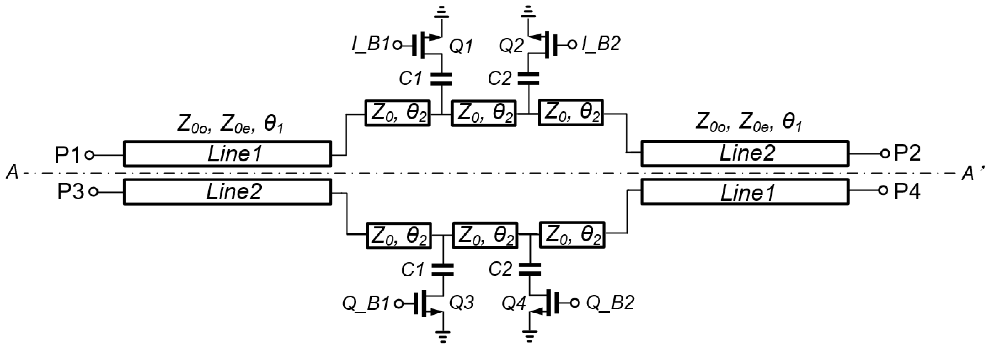
In this article, the quadrature hybrid coupler with digitally reconfigurable I/Q phase is proposed. The circuit schematic diagram is shown in Figure 1, which consists of coupled transmission lines, un-coupled line sections, and switched capacitors. In the un-coupled line sections, one node of the binary weighted capacitors C1/C2 is parallel connected to the I/Q path, and the other node of C1/C2 is connected to the NMOS transistors Q1–4, which are switched on/off by the control voltages I_B1, I_B2, Q_B1, and Q_B2.
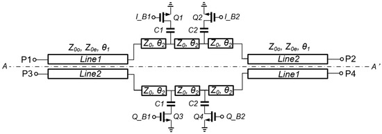
Figure 1.
Circuit diagram of the quadrature hybrid coupler with a digitally reconfigurable I/Q phase.
For the coupled line sections, C12 denotes the mutual capacitance between Line1 and Line2, and Cs1/Cs2 denote the capacitance between Line1/Line2 and ground. The coupling coefficient k can be written as [13]
The proposed quadrature hybrid can be analyzed using even/odd mode theory along A-A’ plane, as shown in Figure 1. The transmission coefficient Te,o, and reflection coefficient Γe,o, can be obtained with the transmission (ABCD) matrix of the several cascaded transmission lines and switched capacitor sections [14],
where Γe,o and Te,o are the reflection coefficient and transmission coefficient in the even/odd mode, and the ABCD matrix of the hybrid coupler in even/odd mode is,
Considering there is an input signal at port P1, the signals emerging on the four ports P1–P4 are,
where (5)–(8) can be used to calculate the return loss, transmission, coupling and isolation parameters of the quadrature hybrid. With (6) and (7), the phase difference between A2 and A3 is the desired quadrature phase,
where the capacitances C1 and C2 are the function parameters. Thus, the phase difference between the transmission port and coupling port can be reconfigured with different C1 and C2 values. The C1 and C2 are implemented with customized interdigital cap in the top thick metal layer for an accurate capacitance value, low loss, and a high quality factor (Q). The cascaded thin-gate NMOS transistors Q1–4 are used as RF switches with the size of 10 μm, to balance between the switch parasitic resistance at on-state and the capacitance at off-state. The source node of the switch transistor is directly grounded for simple DC biasing; thus, a single 0/1.2 V can be used to control the switch at off/on states. Considering the parasitic effects in microwave/RF frequency, the NMOS transistor model and C1/C2 EM-model are co-simulated with the Advanced Design System for the switched binary-weighted capacitance design.
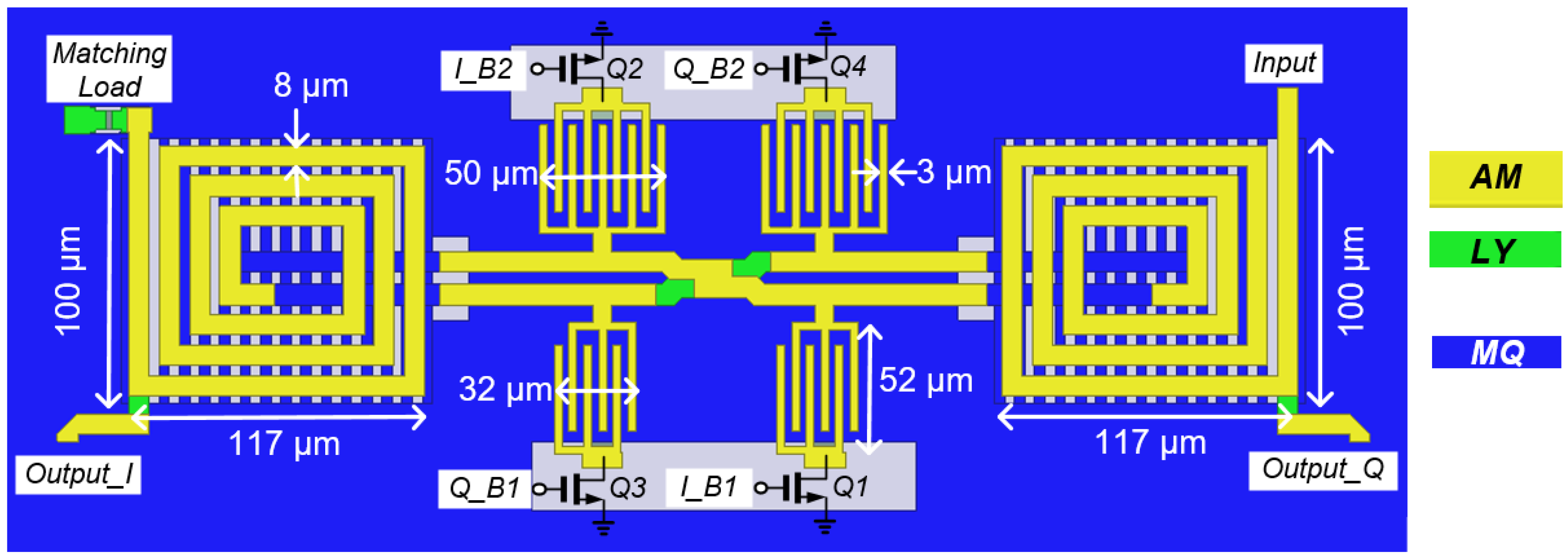
For the coupled line sections, broadside coupling is used for a high coupling coefficient, compact size, and wideband operation [15,16]. As shown in Figure 2, the top thick metal layers (AM and LY) are used for microwave/RF signals, and the MQ layer as ground plane. Line1 is at the AM layer, and Line2 is at the LY layer. With broadside coupled transmission line sections, the coupling coefficient and transmission line impedance can be flexibly controlled. From (1), with C12 >> Cs1,2, a high coupling coefficient of the coupled line can be obtained. To decrease Cs1,2, the ground plane below coupled-line sections is replaced with floating metal bars. The coupled line sections can be winding to further minimize coupler size. The initial design parameters of the quadrature coupler with digitally reconfigurable I/Q phase can be analyzed and calculated using (2)–(9). For example, when all switches are at OFF, with Z0o,e, ϴ1, and ϴ2 values as input, the transmission and coupling characteristics of the quadrature coupler can be derived based on the ABCD matrix with (4)–(8). After several rounds of iterations, the initial values for Z0o,e, ϴ1, and ϴ2 can be determined. Then, the physical parameters W and length of the broadside coupling sections can be determined based on the initial Z0o,e and ϴ1. Finally, the physical parameters are optimized with a full-wave EM-simulator, as shown in Figure 3.
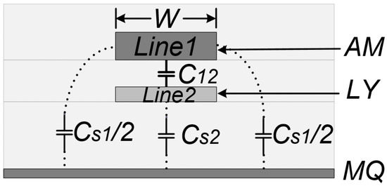
Figure 2.
Cross-section view of the broadside coupled line sections.
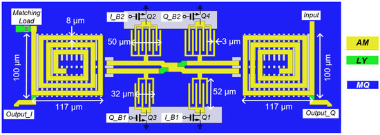
Figure 3.
Top view of the proposed quadrature hybrid with a digitally reconfigurable I/Q phase.
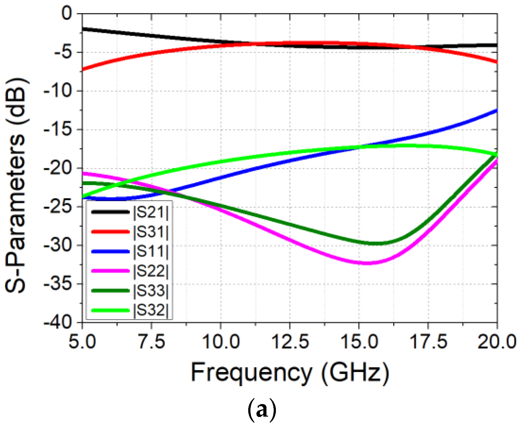
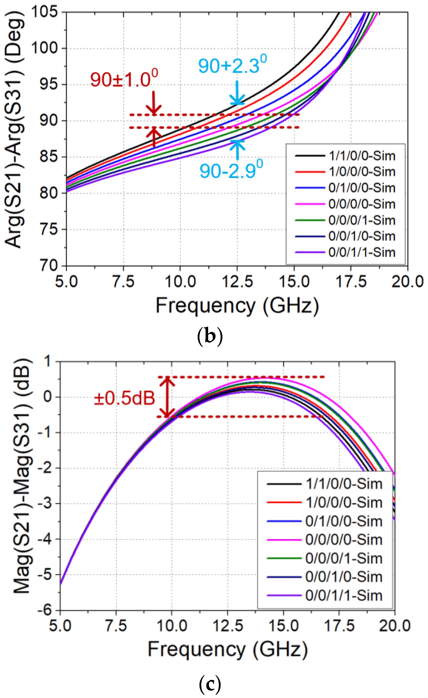
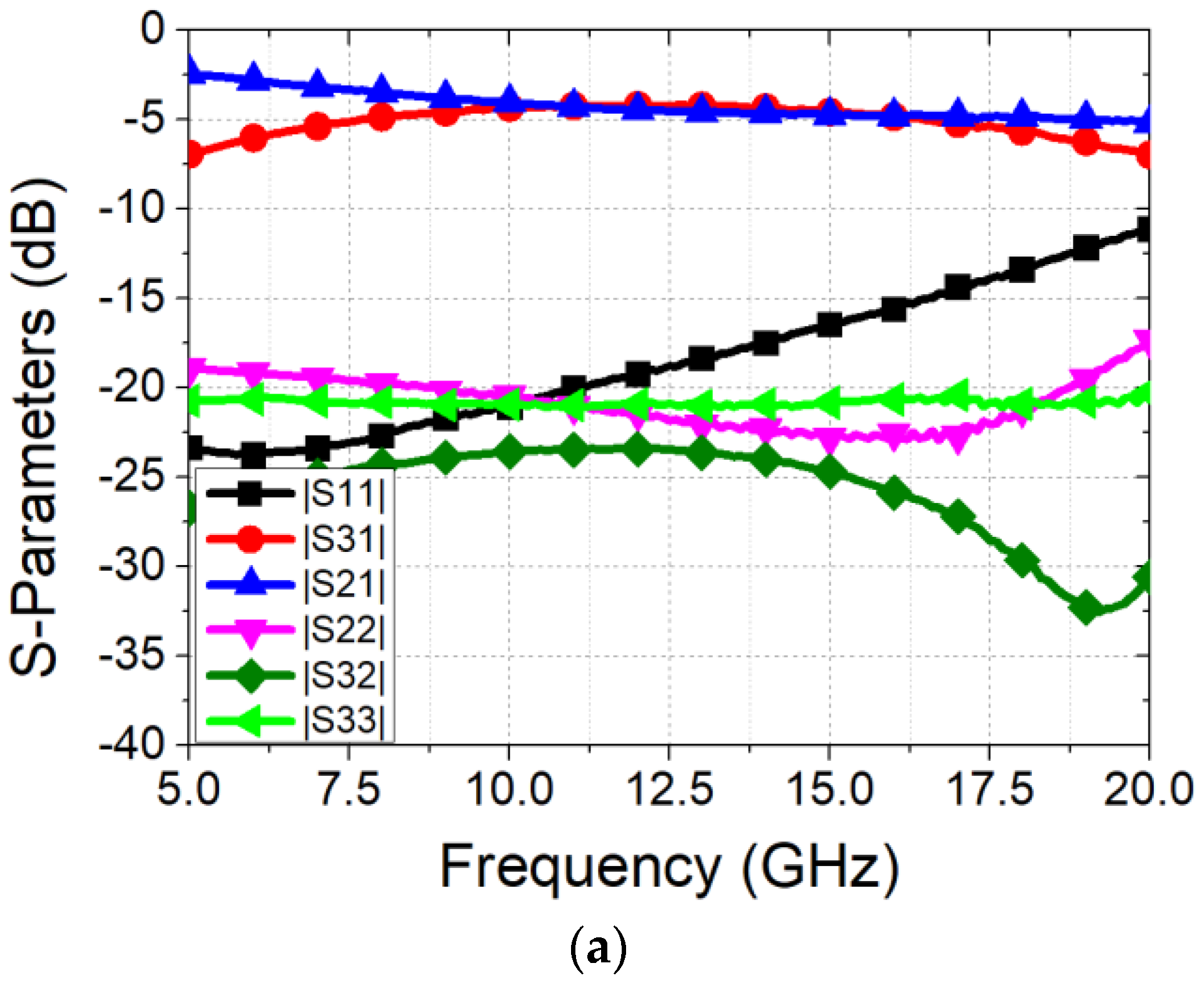
Figure 4 shows the simulated results of the compact quadrature coupler with a digitally reconfigurable I/Q phase. Figure 4a shows the S-parameter of the transmission (S21), coupling (S31), and isolation (S32), when the digital control-bits I_B2/I_B1/Q_B2/Q_B1 are 0/0/0/0 (all switches at OFF). S11, S22, and S33 are the return loss for each port. For 10~15 GHz, the simulated magnitude difference between the S21 and S31 is less than ±0.5 dB, the isolation and the return loss for each port is better than −17.5 dB.

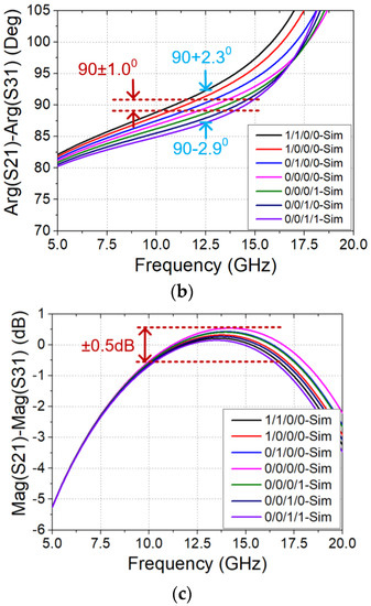
Figure 4.
Simulated results for (a) the S-Parameters of the quadrature hybrid, when digital control bits I_B2/I_B1/Q_B2/Q_B1 are 0/0/0/0 (initial state: all switches at OFF); (b) phase difference between the S21 (transmission) and S31 (coupling), for the seven phase-configuration states; (c) magnitude difference between the S21 (transmission) and S31 (coupling) for the seven phase-configuration states.
Figure 4b,c show the phase and magnitude difference between the S21 and the S31 for all phase-configuration states. It is noted that although there are 16 combinations for the four control bits (I_B2/I_B1/Q_B2/Q_B1), not all of the combinations are valid. For example, the combination 0/1/0/1 means both the I-path C1 and the Q-path C1 are connected to the transmission line when the transistors Q1 and Q3 are switched on. In this case, the phase offset configuration for the I-path and Q-path are canceled with each other. Thus, I_B2/I_B1/Q_B2/Q_B1 need to be grouped as two control bits for the I-path and two control bits for the Q-path, which corresponds to seven valid phase-configuration states, including the initial 0/0/0/0 state (all switches at OFF).
For 10~15 GHz, the phase difference between the S21 and S31 is 90 ± 3.0° for the initial 0/0/0/0 state. With all the seven phase-configuration states, the phase difference can be improved to 90 ± 1.0° for 10~15 GHz, with each configuration state covering a small sub-band, as shown in Figure 4b. Meanwhile, for the frequency at 12.5 GHz, the phase can be reconfigured from 90 − 2.9° to 90 + 2.3° with the seven phase-configuration states, which can be used to compensate the I/Q imbalance existing in other parts of the quadrature circuit, like in the I/Q mixer. For the seven phase-configuration states, the impact on the magnitude difference between the S21 and S31 is quite small and keeps within ±0.5 dB, as shown in Figure 4c.
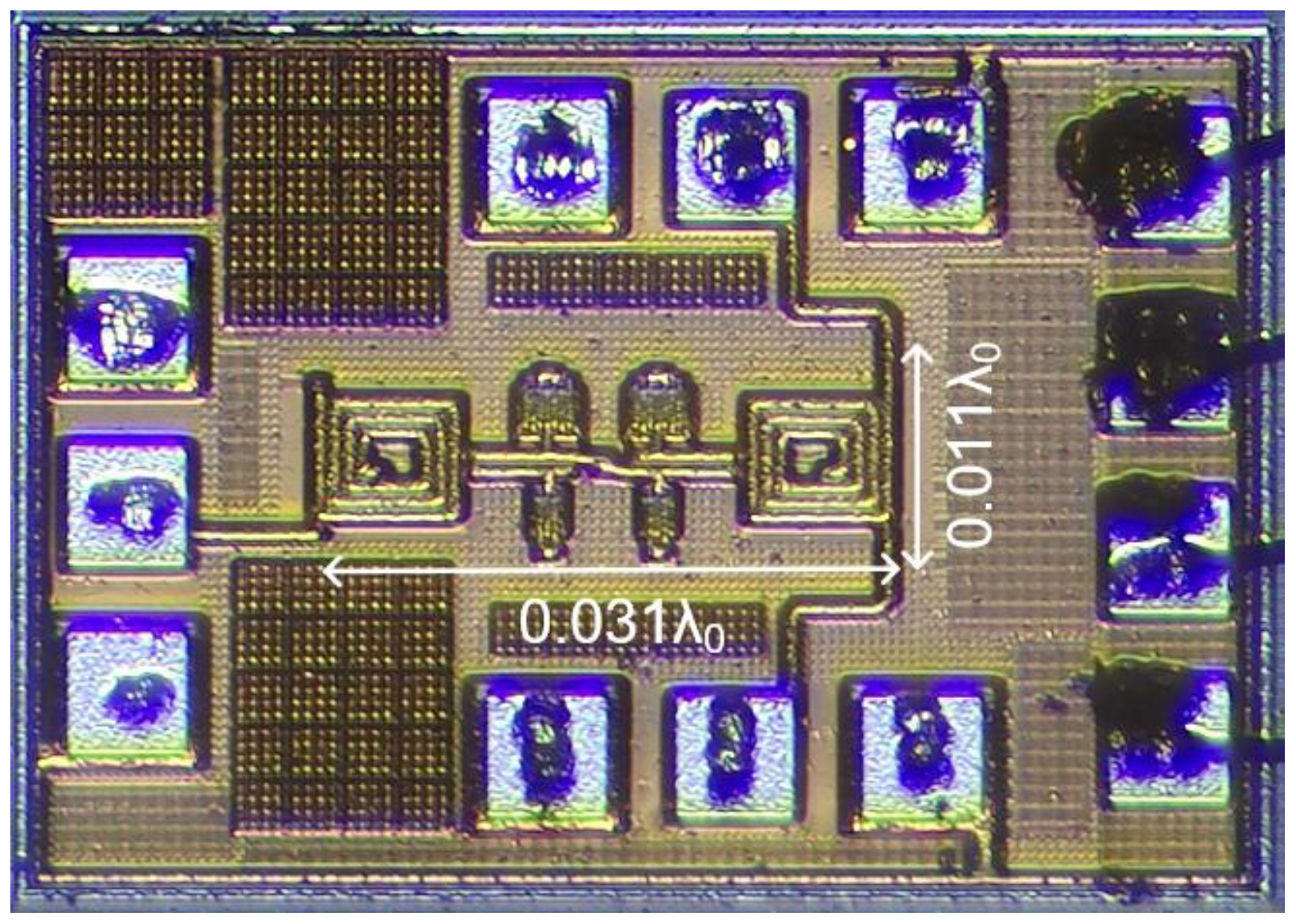
Finally, the compact quadrature coupler is implemented with 130 nm SiGe BiCMOS process. The isolation port is connected with an on-chip 50 Ohm resistor (as the matching load). The chip core area is 460 µm × 151 µm, or 0.031λ0 × 0.011λ0, which is ultra-compact, as shown in Figure 5.

Figure 5.
Chip photograph of the compact quadrature hybrid with a digitally reconfigurable I/Q phase.
3. Measured Results
On-wafer measurements are performed using the probe station for the implemented compact quadrature hybrid with a digitally reconfigurable I/Q phase. The DC control voltages are biased with bonding wires for I_B2/I_B1/Q_B2/Q_B1 nodes, and RF ports are tested with G-S-G probes. During measurement, the three-port quadrature hybrid is directly measured with Keysight Vector Network Analyzer (VNA) N5245B, for the transmission, coupling, isolation, and return loss, respectively. The insertion loss (IL) of the RF connector and cable have been calibrated for the following measured results.
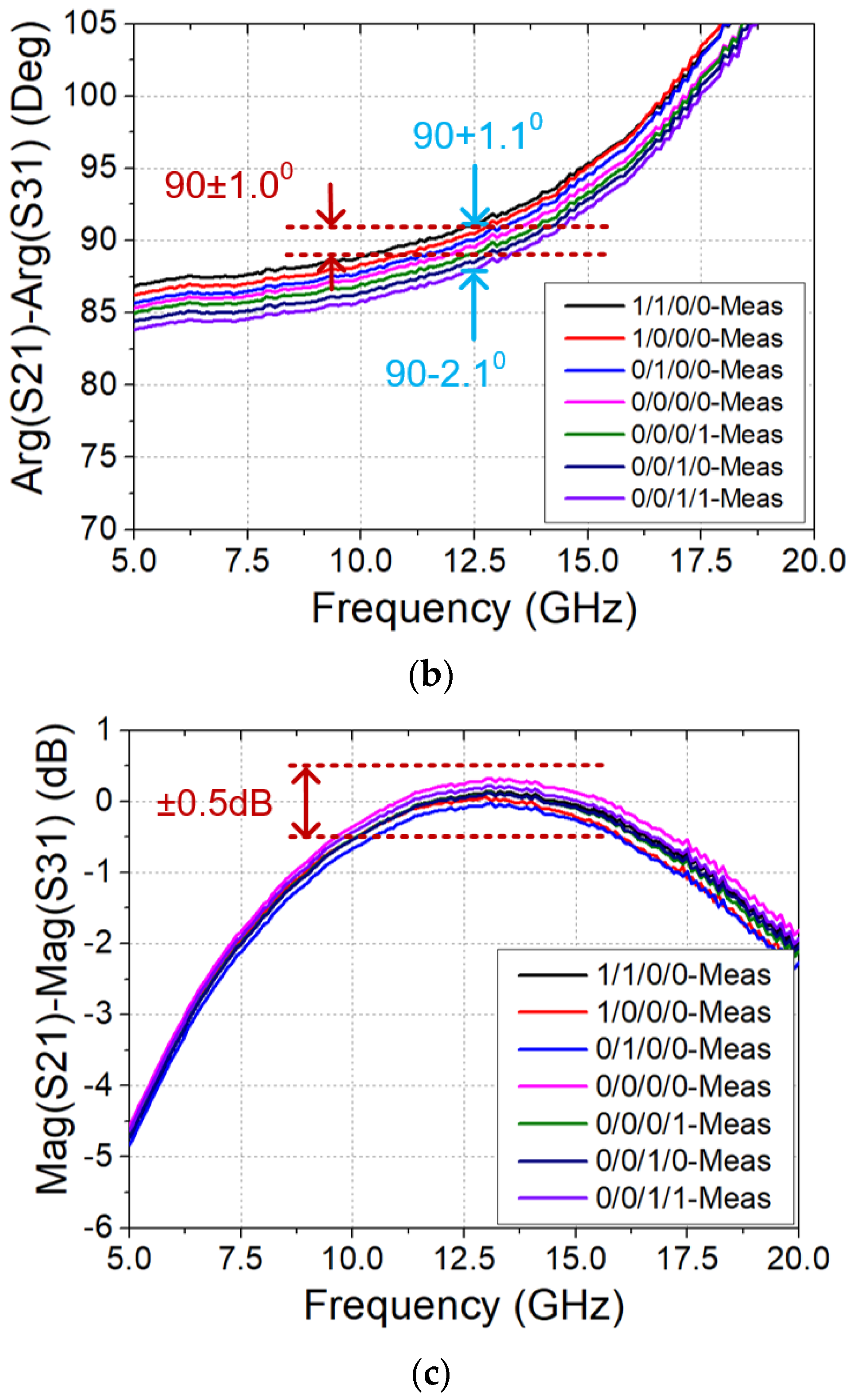
Figure 6a shows the measured results of the compact quadrature coupler with digitally reconfigurable I/Q phase at the initial 0/0/0/0 state (all switches at OFF state). There are some ripples in the measured S-parameters, possibly due to the non-ideal wideband cable and RTL terminations during VNA calibration, for the measured frequency band. In Figure 6a, the S21 (transmission) is −4.1~−4.6 dB, and S31 (coupling) is −4.0~−4.8 dB from 10~15 GHz, or a fractional bandwidth of 40%. Compared to the simulated results in Figure 4a, the operation center frequency of the quadrature hybrid drops by ~1 GHz due to the uncounted routing parasitic effects, and the measured insertion loss and coupling loss are larger in measurements. The measured isolation is better than −23.5 dB, and return loss is below −16.2 dB for the operating band.
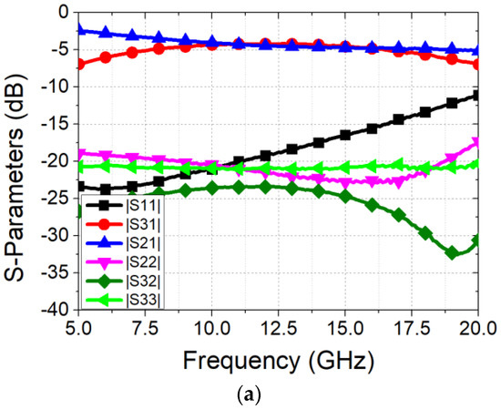

Figure 6.
Measured results for: (a) S-Parameters of the compact quadrature hybrid, when digital control bits I_B2/I_B1/Q_B2/Q_B1 are 0/0/0/0 (initial state: all switches at OFF); (b) phase difference between the S21 (transmission) and S31 (coupling), for the seven phase-configuration states; (c) magnitude difference between the S21(transmission) and S31(coupling) for the seven phase-configuration states.
Figure 6b,c show the measured phase and magnitude difference between the S21 (transmission) and the S31 (coupling) for all seven phase-configuration states. In Figure 6b, for 10~15 GHz, the measured phase difference between the S21 and S31 is 90 ± 3.8° for the 0/0/0/0 state. With all the seven phase-configuration states, the phase difference can be improved to 90 ± 1.0° for 10~14.5 GHz, with each configuration state covering a small sub-band. For compensating purpose, the phase can be reconfigured from 90–2.1° to 90 + 1.1° with the seven phase-configuration states at 12.5 GHz, which can be used to compensate the system I/Q imbalance. For other frequencies in the operation band, the phase reconfiguration range is typically ~3 degrees, which would help to improve the image rejection ratio (IMRR) from −25 dBc to −30 dBc in an I/Q mixer, according to the calculated IMRR v.s. gain and phase error [17]. More phase control bits can be used, if more phase reconfiguration states and a wider phase range are needed. It is noted that the proposed I/Q phase reconfiguration approach has no DC power consumption. Meanwhile, for the seven phase-configuration states, the magnitude difference between the transmission and coupling port is within ±0.5 dB in the measurement, as shown in Figure 6c. The comparison of the reported tunable I/Q phase generator is provided in Table 1.

Table 1.
Comparison of the reported tunable I/Q phase generators.
4. Conclusions
In this article, the development of a compact 10–14.5 GHz quadrature coupler with a digitally reconfigurable I/Q phase in 130 nm SiGe BiCMOS process is presented. Thanks to the switched capacitance loaded on hybrid coupler I/Q path, the quadrature hybrid I/Q phase difference can be optimized and digitally reconfigured. The equivalent model is analyzed with the even/odd mode theory, and the ABCD matrix is used for the circuit derivation. Broadside coupled line sections are used for high coupling coefficient, thus compact coupler size can be easily realized. Measured results show the compact quadrature hybrid has an optimized phase difference of 90 ± 1.0° and an amplitude difference less than ±0.5 dB for 10–14.5 GHz, with the ultra-compact size of 460 µm × 151 µm, or 0.031λ0 × 0.011λ0. Meanwhile, the quadrature hybrid I/Q phase can be digitally reconfigured with the seven phase states for a range of 3 degrees, which can be used to compensate the I/Q phase imbalances in the quadrature system (like in the I/Q mixers), without DC power consumption. It is also noted that for this digital phase reconfiguration approach, more control bits can be used to obtain more phase states and wider phase range if needed.
Author Contributions
Conceptualization, Z.C.; formal analysis, X.X., and D.H.; circuit design, Z.C., P.Z.; validation, J.C., P.Y.; review and editing, Z.C. and J.C. All authors have read and agreed to the published version of the manuscript.
Funding
This research and APC were funded by the National Key Research and Development Program of China under Grant 2019YFB1803202, and National Natural Science Foundation of China, under Grant 62171128.
Conflicts of Interest
The authors declare no conflict of interest.
References
- Peng, X.; Wang, Z.; Mo, J.; Wang, C.; Liu, J.; Yu, F. A Blind Calibration Model for I/Q Imbalances of Wideband Zero-IF Receivers. Electronics 2020, 9, 1868. [Google Scholar] [CrossRef]
- Peng, J.; Zhou, L.; Yao, H.; Yuan, F.; Fang, Z.; Shi, Y. An IQ mismatch calibration and compensation technique for wideband wireless transceivers. J. Semicond. 2014, 35, 085003. [Google Scholar] [CrossRef]
- Hsieh, Y.H.; Hu, W.Y.; Lin, S.; Chen, C.-L.; Li, W.-K.; Chen, S.-J.; Chen, D.-J. An Auto-I/Q Calibrated CMOS Transceiver for 802.11g. IEEE J. Solid-State Circuits 2005, 40, 2187–2192. [Google Scholar] [CrossRef]
- Rosolowski, D.W.; Korpas, P. IQ-imbalance and DC-offfset compensation in ultrawideband Zero-IF receiver. In Proceedings of the 2020 23rd International Microwave and Radar Conference (MIKON), Warsaw, Poland, 5–8 October 2020; pp. 209–213. [Google Scholar]
- Kalyoncu, I.; Ozeren, E.; Burak, A.; Ceylan, O.; Gurbuz, Y. A Phase-Calibration Method for Vector-Sum Phase Shifters Using a Self-Generated LUT. IEEE Trans. Circuits Syst. I Regul. Pap. 2019, 66, 1632–1642. [Google Scholar] [CrossRef]
- Knopik, V.; Moret, B.; Kerherve, E. Integrated Scalable and Tunable RF CMOS SOI Quadrature Hybrid Coupler. In Proceedings of the 12th European Microwave Integrated Circuits Conference, Nuremberg, Germany, 9–12 October 2017; pp. 159–162. [Google Scholar]
- Ma, Q.; Chung, H.; Rebeiz, G.M. A low EVM SiGe BiCMOS 40–100 GHz Direct Conversion IQ Modulator for Multi-Gbps Communications Systems. In Proceedings of the 2018 IEEE Radio Frequency Integrated Circuits Symposium (RFIC), Philadelphia, PA, USA, 10–12 June 2018; pp. 188–191. [Google Scholar]
- Ma, Q.; Chung, H.; Rebeiz, G.M. A 35–105 GHz High Image-Rejection-Ratio IQ Receiver with Integrated LO Doubler and > 40 dB IRR. In Proceedings of the 2018 IEEE/MTT-S International Microwave Symposium (IMS), Philadelphia, PA, USA, 10–12 June 2018; pp. 595–598. [Google Scholar]
- Xu, B.W.; Zheng, S.Y.; Wang, W.M.; Wu, Y.L.; Liu, Y.A. A Coupled Line-Based Coupler with Simultaneously Tunable Phase and Frequency. IEEE Trans. Circuits Syst. I Regul. Pap. 2019, 66, 4637–4647. [Google Scholar] [CrossRef]
- Kuo, C.Y.; Chen, A.Y.; Lee, C.M.; Luo, C.H. Miniature 60 GHz slow-wave CPW branch-line coupler using 90 nm digital CMOS process. Electron. Lett. 2011, 47, 924–925. [Google Scholar] [CrossRef]
- Chen, A.Y.-K.; Liang, H.-B.; Baeyens, Y.; Chen, Y.-K.; Lin, J.; Lin, Y.-S. Wideband mixed lumped-distributed-element 90° and 180° power splitters on silicon substrate for millimetre-wave applications. In Proceedings of the 2008 IEEE Radio Frequency Integrated Circuits Symposium (RFIC), Atlanta, GA, USA, 15–17 June 2008; pp. 449–452. [Google Scholar]
- Chen, Z.; Fan, K. Compact 41–93 GHz symmetric quadrature hybrid based on multi-conductor coupled line in 65 nm CMOS process. Electron. Lett. 2018, 54, 1074–1076. [Google Scholar] [CrossRef]
- Lin, C.S.; Wu, P.S.; Yeh, M.C.; Fu, J.S.; Chang, H.Y.; Lin, K.Y.; Wang, H. Analysis of multiconductor coupled-line Marchand baluns for miniature MMIC design. IEEE Trans. Microw. Theory Tech. 2007, 55, 1190–1199. [Google Scholar] [CrossRef]
- Reed, J.; Wheeler, G.J. A method of analysis of symmetrical fourport networks. IRE Trans. Microw. Theory Tech. 1956, 4, 246–252. [Google Scholar] [CrossRef]
- Chakraborty, S.; Yang, Y.; Zhu, X.; Sevimli, O.; Xue, Q.; Esselle, K.; Heimlich, M. A Broadside-Coupled Meander-Line Resonator in 0.13-µm SiGe Technology for Millimeter-Wave Application. IEEE Electron Device Lett. 2016, 37, 329–332. [Google Scholar] [CrossRef]
- Tran, M.; Nguyen, C. Modified Broadside-Coupled Microstrip Lines Suitable for MIC and MMIC Applications and a New Class of Broadside-Coupled Band-Pass Filters. IEEE Trans. Microw. Theory Tech. 1993, 41, 1336–1342. [Google Scholar] [CrossRef]
- Wu, R.; Minami, R.; Tsukui, Y.; Kawai, S.; Seo, Y.; Sato, S.; Kimura, K.; Kondo, S.; Ueno, T.; Fajri, N.; et al. 64-QAM 60-GHz CMOS Transceivers for IEEE 802.11ad/ay. IEEE J. Solid-State Circuits 2017, 52, 2871–2891. [Google Scholar] [CrossRef]

Publisher’s Note: MDPI stays neutral with regard to jurisdictional claims in published maps and institutional affiliations. |
© 2022 by the authors. Licensee MDPI, Basel, Switzerland. This article is an open access article distributed under the terms and conditions of the Creative Commons Attribution (CC BY) license (https://creativecommons.org/licenses/by/4.0/).