Article

Effect of Large Uniaxial Stress on the Thermoelectric Properties of Microcrystalline Silicon Thin Films

1
Nanomaterials Lab, School of Engineering & Physical Science, Heriot-Watt University, Edinburgh EH14 4AS, UK
2
IEK-5 Photovoltaik, Forschungszentrum Jülich, 52425 Jülich, Germany
3
Department of Aerodynamics and Fluid Mechanics, Brandenburg University of Technology Cottbus-Senftenberg, 03046 Cottbus, Germany
4
Faculty of Mechanical Engineering, National Polytechnic School, Quito 170525, Ecuador
5
Centre for Advanced Manufacturing, University of Technology Sydney, Broadway, Ultimo, NSW 2007, Australia
*
Author to whom correspondence should be addressed.
Electronics 2022, 11(24), 4085; https://doi.org/10.3390/electronics11244085
Submission received: 18 October 2022 / Revised: 25 November 2022 / Accepted: 5 December 2022 / Published: 8 December 2022
(This article belongs to the Section Flexible Electronics)

Abstract

:
This study reports on the behaviour of the thermoelectric properties of n- and p-type hydrogenated microcrystalline silicon thin films (µc-Si: H) as a function of applied uniaxial stress up to ±1.7%. µc-Si: H thin films were deposited via plasma enhanced chemical vapour deposition and thermoelectric properties were obtained through annealing at 200 °C (350 °C) for n-(p-) type samples, before the bending experiments. Tensile (compressive) stress was effective to increase the electrical conductivity of n-(p-) type samples. Likewise, stress induced changes in the Seebeck coefficient, however, showing an improvement only in electron-doped films under compressive stress. Overall, the addition of elevated temperature to the bending experiments resulted in a decrease in the mechanical stability of the films. These trends did not produce a significant enhancement of the overall thermoelectric power factor, rather it was largely preserved in all cases.

1. Introduction

The use of strain to improve transport properties of semiconductor materials is ubiquitous in a number of technologies, [1,2,3,4,5,6] with thermoelectrics (TE) not being an exception. The study of the strain-dependence of TE properties gains even more relevance in the case of flexible materials/devices, which operate under strain most of the time. A number of works have reported the enhancement of TE properties through the introduction of strain in the microstructure of the substrate, and by applying pressure [7,8,9] in commercial materials, however, showing little control over the strain application. To date there has been little research dedicated to revealing the influence of strain on the thermoelectric properties of silicon-based materials. However, strain-inducing defects in silicon, e.g., dislocation loops (DLs), have been shown to have a significant impact on silicon’s thermoelectric properties when present within the crystal lattice, resulting from the significant pressure the DLs exert by pushing-apart nearby Si atoms—this pressure increasing the band-gap local to the dislocation site [10]. This suggests that unravelling these effects further is important. Bearing this in mind, this work aims to determine if tensile or compressive strain drives an increase or reduction in the thermoelectric power factor (PF) in hydrogenated microcrystalline silicon (µc-Si: H) thin films.
There are well-founded reasons to embark on the exploration of this material for flexible thermoelectric applications. First, µc-Si: H is a functional and scalable material recognised in other sectors, i.e., photovoltaics and thin-film transistors (TFTs), with a heterogeneous microstructure that mimics that of nanocomposites. Second, attempts to optimise the power factor of these films deposited on glass substrates have succeeded in previous works in both n- and p-type specimens [10,11]. The ability of the plasma enhanced chemical vapour deposition (PECVD) technique to deposit this material on flexible substrates, widely applied in the photovoltaic and TFTs industry [12,13], opens the possibility to explore its use in flexible TE applications. This approach might also take advantage of the band degeneracy lifting produced by strain when a sample is bent. In fact, improvements of the electrical conductivity (σ) depending on the doping species and strain nature was reported for this material in TFTs [12]. In this study, unlike others in Si for thermoelectrics, that applied theoretically and/or experimentally low strain levels, the TE characterisation is carried out with the sample under large strains.
This research is structured in the following way. Firstly, a detailed study of the total stress generated from deposition and annealing is reported, along with the strain generated due to forced bending. Then, the variations of σ and α in n- and p-type samples, with both tensile and compressive strain, are investigated. Subsequently, another set of samples was used to study the variation of the same properties with the simultaneous effect of strain and temperature. Finally, the expected trends of the power factor for each strain case are reported.

2. Experimental Methodology

The flexible µc-Si: H thin films used for this study were deposited and thermoelectrically optimised based on deposition parameters, following the approach described in previous works [10,11]. The optimised σ, Seebeck coefficient (α) and PF correspond to the as-grown values shown in each figure.
In these µc-Si: H thin films, TE properties could be affected by the different types of stress/strain (s/s) developed during deposition, annealing, and externally applied mechanical loading. For the latter, uniaxial s/s through forced bending has been selected because of the widely reported advantages related to enhancement of transport properties versus biaxial s/s, and because it enables accurate application of strain in both magnitude and direction [14]. The interaction of these stresses/strains results in a total mechanical s/s, which is used for the study of the TE properties.

2.1. Materials Preparation

The fabricated samples started with the deposition of µc-Si: H thin film (1-µm thickness) onto a Kapton HN substrate of 150-µm thickness with the deposition conditions described in [10] for n-, and in [11] for p-type thin-films, respectively. Microstructural characterization of these samples confirmed that the required thickness and composition had been achieved. The reader should refer to ref. [10,11] to observe these data. Then, samples were subjected to an annealing treatment to optimise the PF in anticipation of the results achieved in previous studies [10,11]. This was realised in air using a hot plate stocked with a programmable temperature controller, which allowed a rapid temperature stabilisation. The annealing treatment was applied in the range from 200 to 400 °C for 1 h employing a ramp up time of 8 min for both n- and p-type samples. During the cooling process, the samples remained on the hot plate until they reached room temperature (RT) ~25 °C, which occurred in approximately 2 h. Then, the values of σ and α were measured to determine the optimum annealing temperatures for each sample type.

2.2. Materials Characterization

The residual s/s created during deposition and optimisation was determined indirectly drawing on the Stoney equation [15] through the radius of curvature. This parameter was obtained using a confocal microscopy system stocked with an objective with a magnification of 100×, which is part of the Renishaw (United Kingdom) inVia Raman microscope, to collect the coordinates (x, y) of about 100 points located along the profile of the sample (2 × 1 cm). The acquisition accuracy was in the order of 5 µm based on the image resolution, and considering the total sample thickness of 151 µm (substrate plus film), the maximum error incurred is about 3%. The data points were used to replicate the sample profile in Auto-CAD 2019, and by means of fitting analysis, the radius of curvature was determined. Three samples per sample type, i.e., n-/p-type as-grown and, and n-/p-type annealed, were used to average the final curvature profile.
The σ and α were measured in the zone of maximum stress/strain during bending. This area was determined drawing on a well-known computational model in COMSOL Multiphysics [16]. A tetrahedral grid was generated for a rectangular sample with 98,833 elements with dimensions (length = 2 cm, width 1 cm, thickness = 151 µm). Convergence tests suggested reliable solutions above 50,000 elements. The computation model used a Multifrontal Massively Parallel Sparse direct Solver (MUMPS) with a parametric sweep range (0.125 mm, 0.125 mm, 4 mm) to compute several displacements of the boundaries of the sample. The model investigated a pre-described displacement of both the short edges in the x-direction, and stress/strain on the material. All other surfaces were defined free to move. The computational solver was started considering the ambient temperature at 20 °C, where the Young’s modulus, Poisson’s ratio and density were defined as from the specification catalogue [17].

2.3. Thermoelectric Property Tests

The voltage drop and current were obtained with the device mounted on a Wentworth four-point probe station that enabled the accurate positioning of the electric contacts on the surface of the sample during bending, and arranged according to the Van der Pauw technique. These quantities were measured through a Keithley 2700 digital multimeter and 2661AC/DC current source. Data were obtained at room temperature in air. The sample bending was carried out with a home-built vice-like device. The bend, either convex or concave, was produced by the displacement of the sliding jaw in steps of 0.5 mm per bending cycle. This displacement was controlled through a digital Vernier calliper coupled in the vice. The σ was first determined for each sample (2 × 1 cm) in flat state with probes situated on the corners and in a reduced area in the centre of the sample (maximum stress). The calculation was performed based on the approach developed in [18] for rectangular samples of anisotropic material. The conductivity reported corresponds to principal component in the longitudinal direction, matching with the strain application. Hereafter, all the σ values were determined in the reduced area, first with the sample in bending state, and later in re-flattened state, completing the measurement cycle. This process was repeated for each bending step until the mechanical failure of the sample was reached.
The application of simultaneous uniaxial strain and elevated temperature to determine the σ needed the fabrication of an integrated apparatus. The bending was performed with the aid of convex, and concave cylinders, machined with pre-defined radius of curvature in the range from infinite (flat) down to 6.4 mm. Machining to lower radius of curvature in the concave direction was not possible due to the lack of specialised tools. The heating system comprises of cartridge electrical resistances of 3/8” that are inserted inside the cylinders, and a PID temperature controller, able to reach a maximum temperature of 250 °C. The measurement equipment included a high precision multimeter from Keysight and a current source, a Keithley 2400 AC/DC. For more details on the design of this equipment see [19]. The characterisation of the voltage drop and current was the same as that followed for samples subjected solely to strain, but the data were recorded only when the samples reached steady state at 60 °C.
A Seebeck stage coupled with a vice-like mechanism was built for characterization of samples (2 × 1 cm) under bending conditions. This system consisted of a LakeShore 325 temperature controller with heater and resistance temperature detector that allowed the feedback mechanism with the proportional-integral-derivative (PID) controller, a Linkam LTS420 temperature-controlled stage, two contacting thermocouples, a Keithley 2700 digital multimeter (DMM) and a Keithley 7700 switch card. A steady state temperature method was used that stabilised the sample at a specific temperature difference before the measurement of the signals. Seebeck values were collected in the zone of maximum stress from room temperature up to a maximum of 60 °C in air, in the sequence flat, bending, and re-flattened states until the mechanical failure was reached (similar to the procedure for σ).

3. Results

3.1. Mechanical Stress/Strain Characterisation

The variation of TE properties were evaluated as a function of the total mechanical s/s. This s/s results from the interaction of the residual strain (RS) generated in the film during deposition and the optimisation process, with the s/s produced by the forced bending.

3.1.1. Residual Stress in Flexible µc-Si: H Thin Films

The total RS is reflected in the radius of curvature adopted by the sample after deposition (intrinsic stress), and after optimisation of the PF via annealing. With this correlation, the Stoney’s equation appears suitable to determine the final s/s in the film if complying with certain conditions [20]. It establishes a linear relation of the stress generated in a thin-film with the amount of bending produced in the film/substrate system (radius of curvature) in the following way [15]:
σ s = E s 6 1 v s   h s 2 h f   1 R 1 R 0
where E s = 2.76   GPa , h s = 150 × 10 6   m , and v s = 0.34 are the Young’s modulus, the thickness and the Poisson’s ratio of the substrate, respectively, and h f = 1 × 10 6   m represents the thickness of the film. R and R 0 are the radii of curvature after and before the deposition of the µc-Si: H film on the substrate.
Even though in some cases one or more of such conditions are not strictly compliant, this formula has frequently been applied for determining the stress of similar thin films, i.e., nano-crystalline silicon thin films, and amorphous silicon thin films [20]. In this study, the very low ratio ( β = h f h s = 0.0066 ) along with the rectangular shape of the sample, allowed us to gain more accuracy by augmenting the propensity of it to adopt a spherical shape in bending state. In fact, with this condition, the stress becomes more homogeneous approaching the criterion for the applicability of the Stoney´s equation.
Table 1 illustrates the results of intrinsic and total residual stress produced in the film/substrate system for n- and p-type samples. It is important to remark that owing to the optimisation process carried out to enhance the PF, n-type samples were annealed at 200 °C while p-type samples at 350 °C. For the calculations, R0 was neglected as the Kapton used provided an excellent dimensional stability and flatness at RT. For the sake of comparison with other studies, the widely used convention of assigning a positive value to tensile s/s, and negative to compressive s/s are employed herein.
Table 2a–e illustrates, in sequence, the schematic curvature produced in the film/substrate system due to the stress generated during deposition and TE optimisation, which is explained in the following manner.
In general, from the results it can be observed that after deposition, the samples developed a negative intrinsic s/s independently of the doping nature, which is reflected in the biased bending in the outward direction in agreement with previous results [21,22,23,24]. The intrinsic s/s showed a slighter higher value for n-type (≈−0.33 GPa) samples in comparison to p-type ones (~−0.27 GPa). The negative nature of this stress is likely acquired during film growth due to the deposition technique employed. Ion bombardment was found to be a typical process occurring in PECVD where energetic ions strike the silicon atoms in the subsurface layer with an energy higher than the atomic displacement energy of silicon [25,26,27,28]. As a result, the bonding between silicon atoms is compressed producing a force in the plane of the film as shown in box a) in Table 2; however, as the film is constrained by the substrate, it cannot expand, but instead the substrate can bend. A qualitative estimation of the ion momentum, the parameter that controls ion bombardment, drawing on the correlation developed in [27] gives ~1.48 a.u., and ~1.27 a.u for n- and p-type samples, respectively, in arbitrary units (a.u.). It suggests a slightly higher negative stress formation for n-type films considering its direct relationship with ion momentum, which supports the stress results computed from the curvature measurements.
There are other factors that might contribute to negative stress generation during deposition that cannot be precluded. Hydrogen content, both non-bonded and bonded, have been ascribed as responsible for compressive stress creation in numerous studies regarding PECVD and µc-Si: H [22,29,30,31]. Given the microstructure of this material, that was proven to have a columnar structure and voids in a previous work [10], and the high hydrogen dilution ratio ((H2/SiH4) n: 200; p:133.3), it is probable that non-bonded hydrogen was trapped in these micro-spaces. This stored molecular hydrogen can raise the gas pressure of the micro-voids increasing macroscopically the mechanical stress. Likewise, bonded hydrogen in the form of SiHx species is thought to contribute to negative stress formation [29]. During deposition, atomic hydrogen diffuses into the subsurface zone inserting into strained Si-Si bonds forming Si-H-Si configurations, increasing the compressive stress. Indeed, compressive stress seems to be a requisite for nucleation of µc-Si: H from the amorphous phase, as a direct correlation has been found between hydrogen dilution and stress, which coincides with the transition from amorphous to microcrystalline phase [31].
On the substrate side, other stress effects might appear during deposition that interact with the film stress described above. As the film/substrate system returns to RT after deposition, an additional negative stress is generated on the film due to mismatches of the coefficient of thermal expansion (CTE) between the film and substrate. In fact, the higher CTE of Kapton HN (~×7) with respect to µc-Si: H allows the former to shrink faster when cooling down, applying compressive loads on the film [17,32]. The computing of thermal-induced stress is not straightforward as the CTE of Kapton changes with temperature [33], and because, according to the thermal properties of Kapton HN [34], the substrate was expected to undergo a minimal shrinkage (~0.17%) at 185 °C, further contributing to negative stress.
As was expected, the negative intrinsic stress created during deposition was not definitive, but underwent further changes produced during the optimisation of the PF via thermal annealing that ends in the total residual stress. Overall, it is noticeable that both film types are under a more pronounced negative stress than as-deposited samples showing slightly higher values for p-type (−0.58 GPa) as compared to ~−0.53 GPa for n-type after post-processing, as shown in box e) in Table 2. On the film side, considering that hydrogen has been found to begin diffusing out at temperatures over the deposition temperature (185 °C) [35], annealing likely produced the hydrogen out-diffusion from the microstructure whose amount strongly depends on the exposure time and annealing temperature employed in each case. Consequently, considering the different annealing temperatures used in n- (200 °C) and p- (350 °C) type samples, it is reasonable to presume a higher loss of hydrogen in p-type films. With the loss of hydrogen, the intrinsic negative stress mechanism assumed previously, exerted by both non-bonded and bonded hydrogen in as-grown state, would be reduced leaving the microstructure less compact, and probably originating an additional positive stress due to a reduction in volume that counteracts the initial intrinsic negative stress. In fact, a number of publications reported a correlation between positive stress creation and hydrogen out-diffusion [22,33,36]. Hence, it is plausible to infer that p-type films are left under less negative stress (higher positive stress creation) than n-type films (less positive stress creation) after the optimisation process, as shown in box (c) in Table 2 which seems to contradict the computed values. Nonetheless, the annealing effect on the substrate during optimisation might provide an explanation for the results of total residual stress.
On the substrate side, the same thermal effects identified during deposition might appear in the optimisation process but with higher magnitude, in particular in p-type films. First, a larger thermal-induced stress was probably developed in p-type films due to the obvious higher difference between annealing and RT (ΔT = 350–30 °C) as compared with n-type films (ΔT = 200–30 °C), and also due to a higher expected difference in CTE owing to a diverging behaviour between the µc-Si: H film and Kapton under thermal annealing. In fact, while a decrease in CTE is expected in the film with hydrogen desorption according to [37], an increase in CTE of Kapton with annealing temperature is predicted according to the product specification [34]. Second, a shrinkage process likely continues to happen in the substrate associated with the time the sample is under the effect of higher temperature, which further contributes to a negative stress creation. Therefore, the interaction of stress during deposition and optimisation might explain the slightly higher negative total residual stress in p-type films.
To corroborate the distinct contribution of substrate to the film stress due to the application of a different annealing temperature, the thermal-induced stress in the substrate was isolated. To do this, two film-free Kapton substrates were annealed at the same conditions as n- and p-type samples, and later, the curvature was measured. It was evident that a larger curvature was produced on the sample annealed at 350 °C (~7 m−1) in comparison to the sample annealed at 200 °C (0.63 m−1). This difference, by about one order of magnitude, is probably related to the proximity of the annealing temperature (350 °C) to the glass transition temperature (360 °C) specified for this Kapton type [34], where an increase in molecular motion takes place changing the intrinsic amorphous structure from glassy to a rubber-like state [38]. The schematic of the behaviour of both cases is illustrated in box (d) of Table 2. These results confirm that larger compressive loads are applied on the p-types film by the substrate.

3.1.2. Total Mechanical Strain (Residual plus Forced Bending)

For large strains and rotations such as the ones applied by forced bending, the Stoney correlation does not accurately describe the strain behaviour anymore. Instead, this type of strain ( ε ) as a function of the radius of curvature is described by [39]
ε s u r f a c e = h s + h f 2 R 1 + 2 χ η + χ η 2 1 + η + 1 + χ η
where R is the applied radius of curvature,   χ and η are defined by χ = Y f / Y s and η = h f / h s . Y s and Y f are the Young’s moduli, and h f , h s the thickness with subscripts s and f representing the substrate and film. From the mechanical perspective, the structure of this composite is essentially a bilayer composed of a 1-µm thick microcrystalline silicon layer on top of a 150-µm thick Kapton sheet.
Figure 1a,b shows the total mechanical strain as a function of the radius of curvature. This value was calculated by subtracting (adding) the total negative residual s/s to the strain generated by forced bending in the positive (negative) direction. As the total residual strain showed to be slightly different for n- and p-type films, it was necessary to plot a curve for each film type considering tension and compression. This strain-radius relationship is used to correlate the variation of σ, and α with mechanical s/s.

3.1.3. Zone of Maximum Stress by Forced Bending of the Sample

Figure 2 shows the simulation of stress distribution in a sample under tensile produced by bending. The simulation was carried out considering the dimensions and material properties of the actual sample, and the degrees of bending applied in the experiments. It can be noticed that the maximum stress is produced in the centre of the sample and lessens towards the edges, more strongly in the bending direction than in the transverse direction. For large deformations such as the ones applied in this study (> ±0.7%), the stress and curvature components inevitably vary spatially, but the deliberate bending along the length of the sample (2 × 1 cm), that approaches the uniaxial bending case, diminishes this effect producing a more uniform stress in the transverse direction. This zone of maximum stress is the area where the film will fail with the highest probability with progressive bending, and thus, it is reasonable to measure here the σ to obtain representative results. The area defined for the measurements is a rectangle (1 × 0.5 cm) with the centre in coincidence with the centre of the sample. With these considerations, the σ to be determined is actually an average σ that results from the average stress in the zone of measurements that changes with bending.

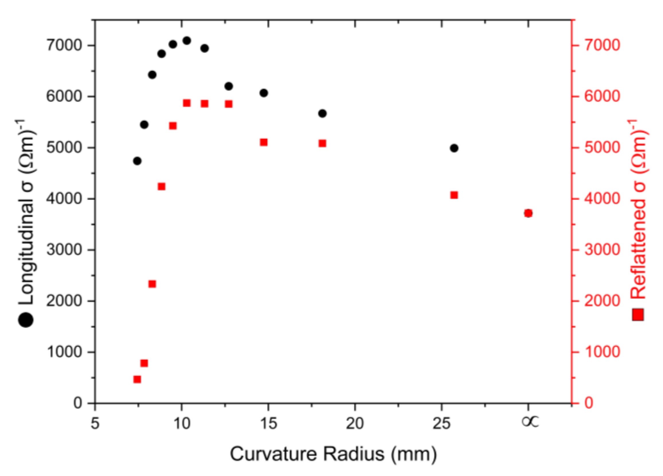
3.2. Electrical Conductivity Characterisation

3.2.1. N-Type µc-Si: H Thin Films under Mechanical Strain

Figure 3 shows the behaviour of both conductivities as a function of radius for positive bending. The plot shows three clear distinct behaviours for the longitudinal conductivity. First, in the range from the infinite radius (flat position/unstrained) down to ~18 mm, this parameter remained at a rather stable value of about 5815 (Ωm)−1. Then, as the strain was increased, an increasing trend also occurred, reaching a maximum of ~7162 (Ωm)−1 at ~9.5 mm, which represents an enhancement of ~23% from its unstrained value. Further strain created an abrupt drop of ~85% from its maximum in the last bending radius, at 8.3 mm. The re-flattened conductivity showed a stable trend indicating a recovery to its initial value of 5815 (Ωm)−1 until a bending radius of ~9.5 mm. Beyond this limit an incremental drop was noted of ~ 10%, and ~49% at ~8.8 mm and ~8.3 mm, respectively, which likely indicates a deterioration of the sample. It is remarkable that the maximum longitudinal conductivity was reached at the same radius (~9.5 mm) where the re-flattened conductivity showed the last data point within the stable trend. This coincidence suggests that for further bending, strain begins to degrade the sample producing structural defects that interfere in the carrier transport, like those shown in Figure S1a of the Supplementary Materials. Hence, it can be inferred that the critical radius at which the conductivity allowed reliable measurements with minimum structural deterioration was ~9.5 mm→ ε (%) = 0.77.
Figure 4 illustrates the behaviour of both conductivities as a function of radius for negative bending. In general, unlike the films under positive strain, it is noted that the longitudinal conductivity describes a decreasing trend in the whole range. It showed a decrease down to 2462 (Ωm)−1 at a radius of ~11.3 mm from its unstrained value 2820 (Ωm)−1. For smaller bending radius it continued to decrease showing some fluctuation reaching a minimum of ~ 2399 (Ωm)−1 at 6.5 mm → ε ~ −1.7%, which means a net fall of ~15% from its unstrained value. It is important to notice that the measurements were increasingly difficult to perform with the reduction in radius as the available space limited the positioning of probes, which might explain such fluctuation. On the other hand, the re-flattened conductivity depicted a stable trend in the whole range with a standard deviation of nearly 40 (Ωm)−1 which means a return to its unstrained value. This feature is essential to demonstrate that the sample has not failed mechanically under the maximum bending radius applied. Thus, based on these results, one can conclude that the critical radius of curvature is located in a smaller bending range (ε (%) > −1.7), which was not possible to reach with the current measurement tools. The state of the sample after characterisation is shown in Figure S1b in the Supplementary Materials.
Experiments were also carried out to measure conductivities as a function of tensile and compressive strain at a temperature of 60 °C, instead of RT. In general, similar trends were obtained in all cases, as shown in Figure S2 of the Supplementary Materials, but showing deviations in the rate of change and the film mechanical resistance. Under tensile strain, σ showed a lower rise ~11% < 23% accompanied by a lower mechanical resistance reflected in a larger critical radius of curvature (35.2 > 9.5 mm) against those samples under strain only. Under compressive strain, σ showed a larger drop ~21% against the 15% for samples under strain only. The larger drop is explained by the reduction in the mechanical resistance of the film. In fact, while samples under strain did not show a mechanical failure for strains >1.7%, the samples under strain at elevated temperature showed a degradation at strains ~0.64%, which is validated by the non-recovery of the re-flattened conductivity.

3.2.2. P-Type µc-Si: H Thin Films under Mechanical Strain

Figure 5 shows the behaviour of the longitudinal and re-flattened conductivity as a function of radius for positive bending. It can be observed that the longitudinal conductivity describes a smooth decreasing trend from its unstrained value of ~2530 (Ωm)−1 down to ~1967 (Ωm)−1 at 12.7 mm. Then, in the next bending step (11.3 mm) the decline accelerates to ~1315 (Ωm)−1 followed by an anomalous fluctuation in the last bending steps ending in ~437 (Ωm)−1. The re-flattened conductivity shows a stable trend down to 11.3 mm. Then, for smaller bending radius a steep decline can be visualised showing a fall of ~81% from its initial value, which suggests that film degradation/cracking started, as depicted in Figure S1c of the Supplementary Materials. Thus, based on these results, it can be determined that the critical radius occurred at 11.3 mm → ε (%) = +0.58.
P-type films were now submitted to a negative stress. Figure 6 shows the behaviour of the longitudinal and re-flattened electrical conductivity as a function of bending radius. In general, both conductivities show a parabolic-like behaviour for a decreasing bending radius. The longitudinal conductivity increased about 90% from its unstrained value (3718 (Ωm)−1) up to a maximum of ~7095 (Ωm)−1 at a radius of 10.3 mm, followed by a fall down to a minimum of 4742 (Ωm)−1 at 7.4 mm. Similarly, the re-flattened conductivity increased form its initial value up to a maximum of 5874 (Ωm)−1 at 10.3 mm, and then showed a decreasing trend down to a minimum of 468 (Ωm)−1 at a radius of 7.4 mm, which represents a drop about 92% from its maximum.
The substantial increase, about 90% in the longitudinal conductivity from its unstrained value, does not look that great if one checks the trend of the re-flattened conductivity in the same range. The non-recovery from the unexpected higher values appears to indicate that it is in a progressive optimisation process due to strain up to a radius of 10.3 mm. With this consideration, the net increase in the longitudinal conductivity would be ~21%. The reasons for the permanent increase in the re-flattened conductivity under compressive strain are not known, however, one can speculate that the gradual strain applied does not completely relax after releasing, but instead induced a permanent change. For the contrary, the decreasing trend of both conductivities is explained by the continued degradation of samples reflected in the fall >92% of the re-flattened conductivity, as is shown in Figure S1d of the Supplementary Materials. If a mechanical failure occurred at 10.3 mm, it is intriguing why the longitudinal conductivity still remains at relative high values, i.e., 4742 (Ωm)−1 at the last bending radius. A probable explanation is likely related to the compressive strain that re-joins separated surfaces of a crack at the moment of the measurements. In this way, a temporal path is provided for current flow while the sample is under compressive strain.
Again, the inclusion of temperature (60 °C) in the experiments provoked a faster decay of the electrical conductivity under tensile strain, and a lower increase under compressive strain (6% < 21%) as a result of the earlier mechanical failure of the film. In fact, the capacity of the film to absorb tensile (compressive) strain without failure reduced from +0.58% → +0.27% (−1.2%→ −0.66%) with temperature. The results are illustrated in Figure S3 of the Supplementary Materials.

3.2.3. Discussion

To the best of the author´s knowledge, no µc-Si: H strain-induced works for the examination of TE properties has been realised. A few works on some silicon-based structures for TE application have been reported [7,40,41], which can be useful to carry out a qualitative comparison. Additionally, detailed studies covering the behaviour of electrical conductivity under strain developed mostly for TFTs and strain gauges are available to contrast the results found herein [1,12,13].
A summary of the impacts of tensile and compressive strain on the electrical conductivity is presented in Table 3. It is expected that the applied uniaxial strain by bending reduces the crystal symmetry varying the effective mass, and lifting the degeneracy of the either the six-fold conduction band minimum or both heavy hole (HH) and light hole (LH) valence bands of silicon, depending on the nature of strain. These effects cause a redistribution of charge carriers amongst the bands [14,41,42]. Accordingly, the increase in longitudinal conductivity in n-type films under tensile strain can be attributed to the energy lifting of the four conduction Δ4 valleys that induced the repopulation of electrons into the lowered Δ2 valleys. In this way, more carriers with lighter effective mass participate in the transport increasing the conductivity. It is remarkable that a lower enhancement (~23%) was achieved in n-type µc-Si: H films as compared to bulk silicon (35%) [40], even though a larger strain was applied in the former (0.77 > 0.2%). This might be related to the different level of carrier concentration (n) and morphology of each material structure. It was reported that to achieve a complete redistribution of occupied states, the applied strain required is proportional to the level of n [40]. Thus, for a higher n as in our films (~4 × 1020 cm−3), a larger strain is required to achieve a similar enhancement as that in bulk silicon (~8 × 1015 cm−3). Likewise, it was demonstrated that µc-Si: H films contain a large number of grain boundaries which are probably softening the strain applied.
For compressive strain the opposite occurs. The decreasing trend observed is probably the result of lifting the Δ2 valleys allowing the transfer of electrons to the lowered four Δ4 valleys giving rise, at the same time, to an increase in effective mass, which in turn, decreases the electrical conductivity. Similarly, under the same compressive strain (0.6%) it can be verified that n-type µc-Si: H films show a minor decrease in conductivity ~5%, against ~15% for bulk silicon [40], giving more support to the softening effect of grain boundaries and the importance of the n.
On the other hand, the physics for the strain-dependent valence bands is more complex because apart from the band splitting, the strain is thought to warp the valence band inducing a change in the effective mass [14]. The decreasing trend shown for p-type µc-Si: H films under tensile strain is likely related to a degeneracy lifting process. It shifts energetically the HH band up, and lowers the LH band with the corresponding repopulation of high energy carriers into the latter, and the alteration of the band curvature. In this way, the dominant band for transport becomes the HH band, which has a relative larger effective mass that reduces the overall conductivity. This trend deviates from the bulk silicon, which shows a slight increase, but is coherent with the reduction reported in [13] for µc-Si based TFTs, which is ascribed to the decrease in the hole mobility.
For compressive strain, the degeneracy lifting is reversed. It is, the LH band becomes the top valence band which contains more light holes to participate in the transport, reducing the effective conductivity mass [40]. As a result, an increasing conductivity trend is appreciated in µc-Si: H films similar to that reported for bulk silicon, but with different rate of change. While an increase of ~23% at ~1% strain was obtained in µc-Si: H films, a larger increase ~40% at a lower strain ~0.6% was reported for bulk silicon. This deviation is probably explained again by the morphological and carrier concentration features of each material structure.
From the results, it is noticeable that either within n-type or p-type films, those samples bent in compressive strain offer a larger mechanical resistance (smaller bending radius) than those bent under tensile strain. It is well known that crack-formation due to tensile strain is produced entirely in the film, whilst delamination due to compressive strain is produced in the film/substrate interface. Regarding that a good adhesion force between the film and substrate was demonstrated for µc-Si: H films deposited via PECVD in a previous work [11], it is not surprising that the system film/substrate failed first in the film.
Finally, in order to confirm that the effect of strain on the electrical properties is via alteration of crystalline grains, it is possible to draw on the Raman technique, which distinguishes the presence of tensile and compressive strain through the shift of the Raman signal to lower and higher values, respectively. The focusing parameters are the same as the ones used in [10]. Figure 7 illustrates the behaviour of Raman shift of a p-type sample as a function of tensile strain. The first point of the plot (522.5 cm−1) represents the Raman frequency in flat position before the bending experiments. The calculation of stress based on [43] gives a stress (~0.62 GPa) very similar to that previously obtained from the analytical Stoney´s method (0.58 GPa). Clearly, this higher Raman shift with respect to the stress free single crystalline Silicon (520.7 cm−1) confirms the total residual compressive stress creation during growth and post-processing. Overall, it can be observed that the Raman-active phonon modes corresponding to the crystalline fraction moves steadily towards lower values with decreasing bending radius in the spectra. It confirms the presence of a local tensile stress in the crystalline grains, which alters the band structure, and gives rise to the change in the electrical conductivity.

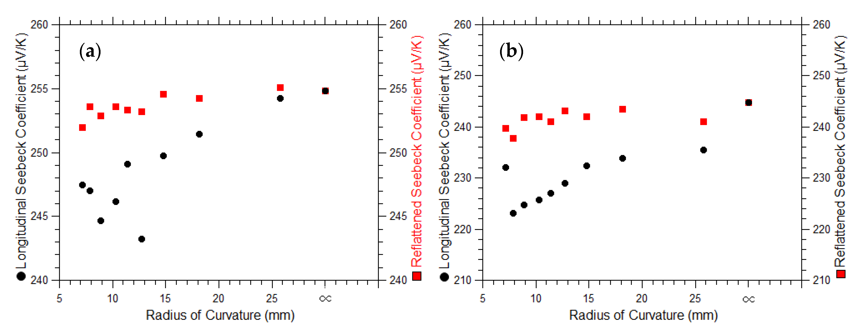
3.3. Seebeck Coefficient under Mechanical Strain

The typical trends described by the Seebeck coefficient vs. temperature are illustrated in Figures S4 and S5 of the Supplementary Materials for n-, and p-type samples, respectively.

3.3.1. N-Type µc-Si: H Thin Films

Figure 8a displays the behaviour of the longitudinal Seebeck coefficient as a function of tensile bending radius and following re-flattening. The longitudinal Seebeck coefficient started at ~−129 µV/K in the unstrained state, and then decreased almost linearly with increasing strain in the whole range reaching a minimum of ~−98 µV/K at a radius of ~6.8 mm → ε (%) ~1.1, which represents a fall of ~24%. A similar behaviour was reported for biaxial-strained silicon in ref. [40] which was ascribed to a degeneracy lifting process. Under sufficient tensile strain, the electrons from the lifted Δ4 pockets repopulate the lowered Δ2 pockets, increasing their occupation. According to the Mott’s relation α ~(n)−2/3 [44], the ratio of redistribution of the carrier concentration (n = 6/2) in the Δ2 pockets induces a reduction in Seebeck ratio (α = 0.48). This decrease is strengthen by an expected lighter effective mass attributed to the Δ2 bands. Compared to bulk silicon at the same strain (~0.2%), the Seebeck coefficient in this work shows a lower decrease (~5 < ~9%), which is likely related to both the higher absorption of the applied stress in the grain boundaries and the different level of n-doping.
Similarly, the behaviour of the longitudinal Seebeck coefficient under compressive strain is shown in Figure 8b, alongside values following re-flattening. Initially, the longitudinal Seebeck remained stable at ~−155.5 µV/K up to a radius of 18 mm, followed but an increasing trend reaching a maximum of ~−175 µV/K at a radius of 6.5 mm, which represents an enhancement of about 13% over its unstrained value. An analogous qualitative enhancement was found in [40], but under a lower strain (−0.25%). The higher strain (6.5 mm →ε (%)= −1.7) needed to maximize the Seebeck is related to both the higher n-doping and the softening of the strain at the grain boundaries as cited in ref. [40]. The repopulation into the lowered Δ4 pockets (n = 6/4) in this strain case according to the Mott’s relation produces a Seebeck ratio of 0.76. This result justifies a less decrease in the Seebeck compared to the tensile case, but not an improvement. The increase should come from the raise of the electron effective mass attributed to the Δ4 pockets under compressive strain as found in [45].
Regarding the re-flattened Seebeck coefficient, it showed a stable trend in the whole range of measurements in both tensile and compressive strain cases. This behaviour would mean that the film did not degrade or fail under the effect of strain and temperature, which contradicts the results found in the conductivity measurements. The explanation is in the measuring technique employed in each property. While conductivity was measured using four-point probe, the Seebeck was measured based on two-probe configuration. It is probable that during the Seebeck measurements cracks already formed, but extended parallel to the path that joins the two probes allowing a flow of carriers, which is more complicated in the case of four probes in a rectangular arrangement.

3.3.2. P-Type µc-Si: H Thin Films

Figure 9a shows the results of the longitudinal Seebeck coefficient as a function of tensile strain and subsequent re-flattening. It can be observed that Seebeck coefficient experienced a slight decreasing trend starting at ~255 µV/K in the unstrained state and reaching a minimum of 247.5 µV/K at a radius of 7.1 mm → ε ~1.1%, which represents a marginal fall ~ 3%. Compared to bulk silicon at the same strain (0.6%), it is noticeable the lower reduction in the Seebeck for µc-Si: H films (3 < ~10) % [40]. This result is explained again by the weaker effect of strain in a material with a higher doping level, and a large density of grain boundaries, as it is µc-Si: H thin films.
The same parameters as a function of compressive radius are illustrated in Figure 9b. The longitudinal Seebeck showed a slight decreasing trend starting at an initial value of ~245 µV/K and running down to 232 µV/K at a bending radius of 7.1 mm → ε ~−1.6%, which represents a drop of around 5%. A similar marginal fall was reported for bulk silicon which was attributed to the redistribution of carriers in the valence band valleys [40].
The small deviation in decay of the Seebeck coefficient under tensile (compressive) strain can be explained by the repopulation of holes from the lifted HH (LH) band into the lowered LH (HH) band in a similar proportion. From Mott’s relation α ~ n−2/3 [44], and assuming a twofold degeneracy for the valence band, the correspondence of the Seebeck ratio to the ratio of redistribution of the carrier concentration (n = 2/1) would be 0.63 for both stress cases. This decrease is counteracted by an expected larger effective mass of the top HH band for the tensile stress case. Again, the re-flattened conductivity shows a stable trend for both strain cases, which is likely explained by the lower sensitivity to cracks of the two probe configuration.
Table 4 summarises the trends of the Seebeck coefficient for all the strain cases, showing the net variation with respect to the unstrained case along with its corresponding strain value. Overall, referring back to the conductivity results, their consistency with the opposite trend is clear in all cases except for p-type under tensile strain, where the conductivity and the Seebeck drop very slightly at the same time. This unusual strain-dependent behaviour is not entirely unexpected. A concurrence decay of both parameters with tensile strain over 0.2% was theoretically predicted in [40] for highly p-doped bulk silicon. Additionally, a concurrent increase in both parameters was demonstrated in p-Bi2Te3 [46] due to the application of pressure, which is equivalent to applying compressive strain. The reasons for such deviations remain an open question, but could be related to a too low increase in the effective mass as a result of the softening in the grain boundaries of the applied stress.

3.4. Impact of Strain on the Power Factor

Given that the strain experiments for conductivity and Seebeck coefficient were carried out on different samples, a qualitative description of PF is given below, rather than a numerical derivation.
Based on the conductivity and Seebeck trends shown in Table 5, along with the correlation ( σ α 2 ) , a good approximation of the PF trends can be obtained. Overall, it can be expected a marginal change in the PF in the cases where the electrical conductivity and Seebeck coefficient showed an opposite trend. The results also showed that only in p-type samples under tensile strain the PF might experience a noticeable drop due to the simultaneous fall of both parameters. Unfortunately, a notably increase in PF might not be achieved through the application of uniaxial strain and temperature in this study; however, in most cases, this is a positive finding for this material in application where the magnitude of strain might vary, i.e., in a system where the TE device undergoes significant flexing. The fact that this parameter remained largely unchanged for large strain values suggests that the power output will be largely indifferent to this variation in strain and will be consistent and predictable.
To summarise the findings, one can conclude that the absolute unstrained PF values from the hole-doped film surpass by about one order of magnitude those from the electron-doped films. Weighting the influence of each parameter on the PF, these difference can be attributed to the larger Seebeck of the hole-doped films despite the relative lower conductivity with respect to the electron-doped films. Likewise, strain demonstrated to change the conductivity and Seebeck, but unfortunately a noticeable enhancement of PF could not be obtained for the range of bending used in this study.
In future the effect of strain on the thermal conductivity will also require investigation. However, thermal conductivity is widely acknowledged as the most difficult thermoelectric property to measure. Apparatus does not currently exist on which samples can be easily strained in a measurable way during testing. In attempting to build a rig of this nature, it was difficult to thermally isolate the sample in a way that it remained independent from the bending apparatus. This factor had too great an influence on the results to yield reliable data.

4. Conclusions

The research field of flexible and even foldable electronics is growing, due to the exciting potential for flexible devices [47,48]. In this study the PF of both n- and p-type µc-Si: H thin films were optimised via annealing treatment at 200 °C and 350 °C, respectively, showing a larger value for p-type samples, along a larger limit of mechanical stability under temperature. A slightly larger total residual stress was found to be created during the deposition and optimisation in p-type films (−0.58 GPa) against that created in n-type films (−0.53 GPa). Overall, the electrical conductivity increased in n-type samples under uniaxial tensile stress, and in p-type samples under uniaxial compressive stress, showing a reverse trend for the conjugated stress cases. On the other side, the Seebeck coefficient showed an opposing trend with the electrical conductivity, as classically expected, in all stress cases except for p-type samples under tensile stress. The inclusion of elevated temperature in the bending experiments, overall, resulted in a decrease in the mechanical resistance of the film reflected in the larger radius of curvature held during the conductivity measurements. The resulting trends of the conductivity and Seebeck coefficient did not translate into a notable increase in the PF with the application of uniaxial stress and temperature combined, however, it is remarkable the stability of this parameter for large stresses. In this study, the Seebeck coefficient could be measured under larger strains higher than the conductivity and showed no failure. Although the PF was only determined qualitatively, it is remarkable the fact that this parameter remained largely unchanged for large strain values for both doping types and both strain directions. In a flexible TE system based on µc-Si: H thin films a positive finding is that in any application where the magnitude of strain might vary, the PF should be insensitive to any variation in strain, meaning TE power output will be consistent and predictable. Users should however be cautious about ensuring high strain levels do not cause film failures during operation.

Supplementary Materials

The following supporting information can be downloaded at: https://www.mdpi.com/article/10.3390/electronics11244085/s1, Figure S1: SEM micrographs of final state of samples after bending experiments for a) n-type under tensile strain, b) n-type under compressive strain, c) p-type under tensile strain, d) p-type under compressive strain, and e) a p-type sample not submitted to bending loads; Figure S2: Variation of the longitudinal and re-flattened electrical conductivity for fixed carrier concentration and temperature (60 °C) as a function of bending radius for n-type samples in a) positive strain, and b) negative strain; Figure S3: Variation of longitudinal and re-flattened electrical conductivity for fixed carrier concentration and temperature (60 °C) as a function of bending radius for p-type samples under a) positive strain, and b) negative strain; Figure S4: Example of the temperature dependence of the Seebeck coefficient in the range from room temperature up to 60°C for n-type samples bent at a radius of 10.3 mm in a) tensile strain b) compressive strain; Figure S5: Temperature dependence of the Seebeck coefficient for p-type samples measured in the range from room temperature up to 60°C under (a) tensile strain, and (b) compressive strain.

Author Contributions

Conceptualization, E.A., V.S. and N.S.B.; methodology, E.A., V.S., P.S.B.S., C.P. and E.D.l.C.; software, P.S.B.S.; validation, E.A. and N.S.B.; formal analysis, E.A., V.S., P.S.B.S., C.P., E.D.l.C. and N.S.B.; investigation, E.A., V.S., P.S.B.S., C.P., E.D.l.C. and N.S.B.; resources, N.S.B., V.S., C.P. and E.D.l.C.; writing—original draft preparation, E.A., V.S., P.S.B.S., C.P., E.D.l.C. and N.S.B.; writing—review and editing, E.A. and N.S.B.; supervision, N.S.B.; project administration, E.A. and N.S.B.; funding acquisition, E.A. and N.S.B. All authors have read and agreed to the published version of the manuscript.

Funding

This research was funded by National Secretary of Science and Technology of Ecuador (SENESCYT) by way of a PhD Studentship (E.A.).

Data Availability Statement

All data is available from the corresponding author by reasonable request.

Conflicts of Interest

The authors declare no conflict of interest.

References

  1. Kuo, P.-C.; Jamshidi-Roudbari, A.; Hatalis, M. Effects of Mechanical Strain on Characteristics of Polycrystalline Silicon Thin-Film Transistors Fabricated on Stainless Steel Foil. J. Disp. Technol. 2009, 5, 202–205. [Google Scholar] [CrossRef]
  2. Lange, D.; i Cabarrocas, P.; Triantafyllidis, N.; Daineka, D. Piezoresistivity of thin film semiconductors with application to thin film silicon solar cells. Sol. Energy Mater. Sol. Cells 2016, 145, 93–103. [Google Scholar] [CrossRef]
  3. Li, J.; Shan, Z.; Ma, E. Elastic strain engineering for unprecedented materials properties. MRS Bull. 2014, 39, 108–114. [Google Scholar] [CrossRef] [Green Version]
  4. Thompson, S.; Armstrong, M.; Auth, C.; Cea, S.; Chau, R.; Glass, G.; Hoffman, T.; Klaus, J.; Ma, Z.; Mcintyre, B.; et al. A Logic Nanotechnology Featuring Strained-Silicon. IEEE Electron Device Lett. 2004, 25, 191–193. [Google Scholar] [CrossRef]
  5. Hajji, M.; Absike, H.; Labrim, H.; Ez-Zahraouy, H.; Benaissa, M.; Benyoussef, A. Strain effects on the electronic and thermoelectric properties of Bi2Te3: A first principles study. Comput. Condens. Matter 2018, 16, e00299. [Google Scholar] [CrossRef]
  6. Kusagaya, K.; Hagino, H.; Tanaka, S.; Miyazaki, K.; Takashiri, M. Structural and Thermoelectric Properties of Nanocrystalline Bismuth Telluride Thin Films Under Compressive and Tensile Strain. J. Electron. Mater. 2014, 44, 1632–1636. [Google Scholar] [CrossRef]
  7. Murphy-Armando, F. Enhancement of the electronic thermoelectric properties of bulk strained silicon-germanium alloys using the scattering relaxation times from first-principles calculations. J. Appl. Phys. 2019, 126, 215103. [Google Scholar] [CrossRef] [Green Version]
  8. Pei, Y.; Shi, X.; LaLonde, A.; Wang, H.; Chen, L.; Snyder, G.J. Convergence of electronic bands for high performance bulk thermoelectrics. Nature 2011, 473, 66–69. [Google Scholar] [CrossRef] [Green Version]
  9. Liu, W.; Tan, X.; Yin, K.; Liu, H.; Tang, X.; Shi, J.; Zhang, Q.; Uher, C. Convergence of conduction bands as a means of enhancing thermoelectric performance of n-type Mg2Si(1−x)Sn(x) solid solutions. Phys. Rev. Lett. 2012, 108, 166601. [Google Scholar] [CrossRef] [Green Version]
  10. Bennett, N.S.; Byrne, D.; Cowley, A.; Neophytou, N. Dislocation loops as a mechanism for thermoelectric power factor enhancement in silicon nano-layers. Appl. Phys. Lett. 2016, 109, 173905. [Google Scholar] [CrossRef]
  11. Acosta, E.; Wight, N.; Smirnov, V.; Buckman, J.; Bennett, N. Hydrogenated Nano-/Micro-Crystalline Silicon Thin-Films for Thermoelectrics. J. Electron. Mater. 2018, 47, 3077–3084. [Google Scholar] [CrossRef]
  12. Acosta, E.; Smirnov, V.; Szabo, P.S.B.; Buckman, J.; Bennett, N.S. Optimizing Thermoelectric Power Factor in p-Type Hydrogenated Nano-crystalline Silicon Thin Films by Varying Carrier Concentration. J. Electron. Mater. 2019, 48, 2085–2094. [Google Scholar] [CrossRef]
  13. Janfaoui, S.; Simon, C.; Coulon, N.; Mohammed-Brahim, T. Behavior of the parameters of microcrystalline silicon TFTs under mechanical strain. Solid-State Electron. 2014, 93, 1–7. [Google Scholar] [CrossRef] [Green Version]
  14. Haug, F.; Terrazzoni-Daudrix, V.; Söderström, T.; Niquille, X.; Bailat, J.; Ballif, C. Flexible microcrystalline silicon solar cells on periodically textured plastic substrates. In Proceedings of the 21st EU PVSEC, Dresden, Germany, 4–8 September 2006. [Google Scholar]
  15. Sun, Y.; E Thompson, S.; Nishida, T. Physics of strain effects in semiconductors and metal-oxide-semiconductor field-effect transistors. J. Appl. Phys. 2007, 101, 104503. [Google Scholar] [CrossRef]
  16. COMSOL AB. COMSOL Multiphysics v5.6. Available online: www.comsol.com (accessed on 4 December 2022).
  17. DuPont Kapton Polyimide Film General Specification. Available online: https://www.dupont.com/content/dam/dupont/amer/us/en/products/ei-transformation/documents/EI-10167-Kapton-General-Specifications.pdf (accessed on 4 December 2022).
  18. Price, W.L.V. Electric potential and current distribution in a rectangular sample of anisotropic material with application to the measurement of the principal resistivities by an extension of van der Pauw’s method. Solid-State Electron. 1973, 16, 753–762. [Google Scholar] [CrossRef]
  19. De la Cadena, E.; Pillajo, C. Facultad de Ingeniería Mecánica; EPN: Quito, Ecuador, 2019; p. 172. [Google Scholar]
  20. Ngo, D.; Feng, X.; Huang, Y.; Rosakis, A.J.; Brown, M.A. Thin film/substrate systems featuring arbitrary film thickness and misfit strain distributions. Part I: Analysis for obtaining film stress from non-local curvature information. Int. J. Solids Struct. 2007, 44, 1745–1754. [Google Scholar] [CrossRef] [Green Version]
  21. Christova, K.; Alexandrova, S.; Abramov, A.; Valcheva, E.; Ranguelov, B.; Longeaud, C.; Reynolds, S.; i Cabarrocas, P.R. Structure-related strain and stress in thin hydrogenated microcrystalline silicon films. J. Phys. Conf. Ser. 2010, 253, 012056. [Google Scholar] [CrossRef] [Green Version]
  22. Kroll, U.; Meier, J.; Shah, A.; Mikhailov, S.; Weber, J. Hydrogen in amorphous and microcrystalline silicon films prepared by hydrogen dilution. J. Appl. Phys. 1996, 80, 4971–4975. [Google Scholar] [CrossRef]
  23. Stratakis, E.; Spanakis, E.; Tzanetakis, P.; Fritzsche, H.; Guha, S.; Yang, J. Photoinduced stress in hydrogenated amorphous silicon films. Appl. Phys. Lett. 2002, 80, 1734–1736. [Google Scholar] [CrossRef]
  24. Paillard, V.; Puech, P.; Cabarrocas, P. Measurement of stress gradients in hydrogenated microcrystalline silicon thin films using Raman spectroscopy. J. Non-Cryst. Solids 2002, 299, 280–283. [Google Scholar] [CrossRef]
  25. Fu, Y.Q.; Luo, J.K.; Milne, S.B.; Flewitt, A.J.; Milne, W.I. Residual stress in amorphous and nanocrystalline Si films prepared by PECVD with hydrogen dilution. Mater. Sci. Eng. B 2005, 124, 132–137. [Google Scholar] [CrossRef]
  26. Glew, A.D.; Saha, R.; Kim, J.S.; Cappelli, M.A. Ion energy and momentum flux dependence of diamond-like carbon film synthesis in radio frequency discharges. Surf. Coat. Technol. 1999, 114, 224–229. [Google Scholar] [CrossRef]
  27. Johlin, E.; Tabet, N.; Castro-Galnares, S.; Abdallah, A.; Bertoni, M.; Asafa, T.; Grossman, J.; Said, S.; Buonassisi, T. Structural origins of intrinsic stress in amorphous silicon thin films. Phys. Rev. B (Condens. Matter Mater. Phys.) 2012, 85, 075202. [Google Scholar] [CrossRef] [Green Version]
  28. Davis, C.A. A simple model for the formation of compressive stress in thin films by ion bombardment. Thin Solid Films 1993, 226, 30–34. [Google Scholar] [CrossRef]
  29. Wehrspohn, R.B.; Deane, S.C.; French, I.D.; Gale, I.; Hewett, J.; Powell, M.J.; Robertson, J. Relative importance of the Si–Si bond and Si–H bond for the stability of amorphous silicon thin film transistors. J. Appl. Phys. 2000, 87, 144–154. [Google Scholar] [CrossRef]
  30. Marques, F.C.; Wickboldt, P.; Pang, D.; Chen, J.H.; Paul, W. Stress and thermomechanical properties of amorphous hydrogenated germanium thin films deposited by glow discharge. J. Appl. Phys. 1998, 84, 3118–3124. [Google Scholar] [CrossRef] [Green Version]
  31. Fujiwara, H.; Kondo, M.; Matsuda, A. Nucleation mechanism of microcrystalline silicon from the amorphous phase. J. Non-Cryst. Solids 2004, 338, 97–101. [Google Scholar] [CrossRef]
  32. Schicho, S. Amorphous and Microcrystalline Silicon Applied in Very Thin Tandem Solar Cells; Forschungszentrum Jülich GmbH: Jülich, Germany, 2011; p. 141. [Google Scholar]
  33. Mani, S.; Saif, T. Stress development in plasma-deposited silicon dioxide thin-films due to hydrogen evolution. Thin Solid Films 2007, 515, 3120–3125. [Google Scholar] [CrossRef]
  34. DuPont. Available online: www.dupont.com/content/dam/dupont/amer/us/en/products/ei-transformation/documents/DEC-Kapton-HN-datasheet.pdf (accessed on 4 December 2022).
  35. Bronsveld, P.C.P.; van der Wagt, H.J.; Rath, J.K.; Schropp, R.E.I.; Beyer, W. Post-deposition thermal annealing studies of hydrogenated microcrystalline silicon deposited at 40 °C. Thin Solid Films 2007, 515, 7495–7498. [Google Scholar] [CrossRef]
  36. Temple-Boyer, P.; Scheid, E.; Faugere, G.; Rousset, B. Residual stress in silicon films deposited by LPCVD from disilane. Thin Solid Films 1997, 310, 234–237. [Google Scholar] [CrossRef]
  37. Takimoto, K.; Fukuta, A.; Yamamoto, Y.; Yoshida, N.; Itoh, T.; Nonomura, S. Linear thermal expansion coefficients of amorphous and micro crystalline silicon films. J. Non-Cryst. Solids 2002, 299, 314–317. [Google Scholar] [CrossRef]
  38. Alfredo Campo, E. Selection of Polymeric Materials; Alfredo Campo, E., Ed.; William Andrew Publishing: Norwich, NY, USA, 2008; pp. 103–140. [Google Scholar]
  39. Gleskova, H.; Hsu, P.I.; Xi, Z.; Sturm, J.C.; Suo, Z.; Wagner, S. Field-effect mobility of amorphous silicon thin-film transistors under strain. J. Non-Cryst. Solids 2004, 338–340, 732–735. [Google Scholar] [CrossRef]
  40. Hinsche, N.F.; Mertig, I.; Zahn, P. Effect of strain on the thermoelectric properties of silicon: An ab initio study. J. Phys. Condens. Matter 2011, 23, 295502. [Google Scholar] [CrossRef] [PubMed] [Green Version]
  41. Hinsche, N.F.; Mertig, I.; Zahn, P. Thermoelectric transport in strained si and si/ge heterostructures. J. Phys. Condens. Matter 2012, 24, 275501. [Google Scholar] [CrossRef] [PubMed] [Green Version]
  42. Dziekan, T.; Zahn, P.; Meded, V.; Mirbt, S. Theoretical calculations of mobility enhancement in strained silicon. Phys. Rev. B 2007, 75, 195213. [Google Scholar] [CrossRef]
  43. Annastassakis, E. Physical problems in microelectronics. In Proceedings of the Fourth International School ISPPM, Varna, Bulgaria, 12–18 May 1985; p. 128. [Google Scholar]
  44. Cutler, M.; Mott, N.F. Observation of anderson localization in an electron gas. Phys. Rev. 1969, 181, 1336–1340. [Google Scholar] [CrossRef]
  45. Sajjad, R.N.; Alam, K.; Mohd, K.Q.D. The effects of doping, gate length, and gate dielectric on inverse subthreshold slope and on/off current ratio of a top gate silicon nanowire transistor. In Proceedings of the 2008 International Conference on Electrical and Computer Engineering, Dhaka, Bangladesh, 20–22 December 2008; pp. 283–286. [Google Scholar]
  46. Ovsyannikov, S.V.; Shchennikov, V.V.; Vorontsov, G.V.; Manakov, A.Y.; Likhacheva, A.Y.; Kulbachinskii, V.A. Giant improvement of thermoelectric power factor of Bi2Te3 under pressure. J. Appl. Phys 2008, 104, 053713. [Google Scholar] [CrossRef] [Green Version]
  47. Zan, G.; Wu, T.; Zhu, F.; He, P.; Cheng, Y.; Chai, S.; Wang, Y.; Huang, X.; Zhang, W.; Wan, Y. A biomimetic conductive super-foldable material. Matter 2021, 4, 3232. [Google Scholar] [CrossRef]
  48. Zan, G.; Wu, T.; Dong, W.; Zhou, J.; Tu, T.; Xu, R.; Chen, Y.; Wang, Y.; Wu, Q. Two-Level Biomimetic Designs Enable Intelligent Stress Dispersion for Super-Foldable C/NiS Nanofiber Free-Standing Electrode. Adv. Fiber Mater. 2022, 4, 1177–1190. [Google Scholar] [CrossRef]
Figure 1. Total positive (tensile) and negative (compressive) mechanical strain vs. radius of curvature for (a) n-type and (b) p-type µc-Si: H thin film calculated using Equation (2), and schematic for the tensile (c) and compressive (d) bending direction.
Electronics 11 04085 g001
Figure 2. Numerical simulation of the stress distribution due to tensile stress for a µc-Si: H sample showing the zone of maximum stress. This was carried out generating a tetrahedral grid with 98,833 elements in a stationary mode as described in the experimental section.
Electronics 11 04085 g002
Figure 3. Behaviour of longitudinal and reflattened conductivity versus radius for positive bending at room temperature (20 °C). The former showed an enhancement about 23% at 9.5 mm before an abrupt fall beyond this critical radius of curvature. The latter does not recover its initial values for radius smaller than 9.5 mm.
Electronics 11 04085 g003
Figure 4. Behaviour of longitudinal and re-flattened conductivity with radius for negative bending, at room temperature (20 °C). The former showed a decreasing trend reaching a minimum of 2399 (Ωm)−1 at 6.5 mm, while the latter remained stable in the whole range showing no mechanical failure.
Electronics 11 04085 g004
Figure 5. Behaviour of longitudinal and re-flattened conductivity with radius for positive bending measured at room temperature (20 °C). The longitudinal conductivity shows a decreasing trend reaching a minimum of ~1315 (Ωm)−1 at the critical radius of 11.3 mm, which is corroborated by the abrupt fall of the re-flattened conductivity for smaller radius.
Electronics 11 04085 g005
Figure 6. Longitudinal and re-flattened electrical conductivity variation of p-type films at room temperature as a function of radius for negative bending. The longitudinal conductivity shows a net enhancement of about 21% from its optimised unstrained value. The non-recovery of the re-flattened conductivity suggests that the critical radius takes place at 10.3 mm.
Electronics 11 04085 g006
Figure 7. Bending Raman shift as a function of radius for tensile (positive) bending for a p-type sample. The Raman shift moves to lower values with decreasing radius suggesting the creation of a local tensile strain in the crystalline grains.
Electronics 11 04085 g007
Figure 8. (a,b) Variation of the longitudinal and re-flattened Seebeck coefficient as a function bending radius measured at a fixed temperature of 60 °C for n-type samples (a) under tensile strain, (b) under compressive strain.
Electronics 11 04085 g008
Figure 9. (a,b) Variation of the longitudinal and re-flattened Seebeck coefficient as a function of bending radius measured at a fixed temperature of 60 °C for p-type samples under (a) tensile strain, and (b) compressive strain.
Electronics 11 04085 g009
Table 1. Intrinsic and total residual stress generated during deposition and after TE optimisation via annealing, respectively, with Rr and Rt as the radius of curvature measured for the former and latter, based on the methodology described in the experimental section.
Sample TypeRr (m)Rt (m)Intrinsic Stress (GPa)Total Residual Stress (GPa)
N0.0480.030−0.328−0.527
P0.0590.027−0.265−0.584
Table 2. Bending steps of the film/substrate system produced by the stress/strain created during deposition and optimisation process. Different curvatures were found depending on the doping type, and annealing conditions. RN and RP represent the radius of curvature of the n- and p-type sample, respectively, and the curvature is determined as the inverse of the radius (1/R).
Outward bending due to compressive stressElectronics 11 04085 i001
As-grown stateN-typeP-type
Compressive stress
RN < RP
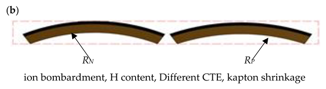
Electronics 11 04085 i002
AnnealingN-type: (200 °C)P-type: (350 °C)
Expected behaviour of the film curvature due to annealing
RN < RP
Electronics 11 04085 i003
Isolation of substrate curvature due to annealing
RP < RN
Electronics 11 04085 i004
Final curvature
RP < RN
Electronics 11 04085 i005
Table 3. Trend of longitudinal electrical conductivity of n- and p-type µc-Si: H thin films under tensile and compressive stress showing the corresponding strain at the critical bending radius (εC).
DopingTensile StrainCompressive Strain
TrendεC (%) TrendεC (%)
NIncrease↑~0.77Decrease ↓>−1.7
PDecrease↓~0.58Increase ↑~−1.2
Table 4. Trends of the Seebeck coefficient for n-and p-type µc-Si: H showing the maximum strain applied during the measurements.
DopingTensile StrainCompressive Strain
Trendε (%)Trendε (%)
Ndecrease (24%) ↓~1.1Increase (13%) ↑~−1.7
PDecrease (3%) ↓~1.1Increase (5%) ↓~−1.6
Table 5. Implications of the trends described by the electrical conductivity and Seebeck coefficient on the power factor.
ParameterN-Type P-Type
(+) Strain(−) Strain(+) Strain(−) Strain
σ
α
PF~invariable~invariable~invariable
Publisher’s Note: MDPI stays neutral with regard to jurisdictional claims in published maps and institutional affiliations.

