Article

A Class-F Based Power Amplifier with Optimized Efficiency in Triple-Band

1
China Academy of Space Technology (Xi’an), Xi’an 710100, China
2
School of Electronics and Information Engineering, Xi’an Jiaotong University, Xi’an 710049, China
3
School of Aeronautics and Astronautics, Zhejiang University, Hangzhou 310058, China
*
Author to whom correspondence should be addressed.
Electronics 2022, 11(3), 310; https://doi.org/10.3390/electronics11030310
Submission received: 30 November 2021 / Revised: 17 January 2022 / Accepted: 17 January 2022 / Published: 19 January 2022
(This article belongs to the Special Issue EMC Analysis in Wireless Communication)

Abstract

:
A Class-F mode-based power amplifier (PA) with optimized efficiency in triple-band was designed using a simple and systematic approach. By considering the second and third harmonic terminations of the PA, the relationship between the output impedance design space and the drain efficiency (DE) is extracted by large-signal model simulation. Then, a low-pass matching topology is utilized for the triple-band efficiency optimization. The method is justified by both simulation and measurement of a triple-band PA to integrate three functions into one hardware, i.e., 1518–1525 MHz for mobile communication, 2.1 GHz for telemetry and control, and 2.492 GHz for navigation signal transport. The proposed PA achieves a measured result of high DE (63% at 1.52 GHz, 71% at 2.1 GHz, 59% at 2.492 GHz) in the three bands with an output power of at least 40 dBm.

1. Introduction

Today, to address the increasing demands of modern wireless communication terminals, it is necessary to cover different standards with a single piece of hardware, and thus, a multi-band transmitter is a key technical challenge [1,2,3,4,5]. To achieve dual-band or multi-band operation with one highly efficient power amplifier (PA) circuit, the design does not only need the correct fundamental loads transformation, but also the proper higher harmonic impedance terminations [6,7].
A common approach to address this problem is to design a broadband PA that covers all the operation bands [7,8,9,10,11]. The fundamental impedance matching with 50-Ohm load is the first step to overcome. Additionally, the second and the third harmonic load terminations also need to be considered to improve the efficiency by various approaches. However, most of the designs failed to solve the challenge and to realize the optimization in operating multi-bands, e.g., the methods proposed in [11,12,13,14] are focusing on the broadband performance, rather than the bands of interest in our application [15,16,17,18,19,20].
The idealized Class-F mode is termed as a waveform of a squared-up voltage wave, which contains only fundamental components, odd higher harmonic components and a half-wave rectified sinusoidal current waveform at its intrinsic current source (Igen) [1,2]. With an infinite number of harmonics, an ideal drain efficiency (DE) of 100% can be obtained and the voltage waveform can be a perfect square waveform. When the controlled harmonic impedances up to the third order, the DE can achieve π / 4 × 2 / 3 (90.7%), and the fundamental output power will increase 2 / 3 (0.6 dB) in the maximum efficiency condition [1,2]. Figure 1 shows the waveform and the load-line of the idealized and the realistic 10-watts transistor used in this paper, namely Cree 10-W gallium nitride high electron mobility transistor (GaN HEMT), CGH40010F. As described in Figure 1, the voltage sweep range of the real transistor is smaller than the idealized condition because of the knee-effect, which will reduce the output power and also the DE as shown in Table 1, from 42 dBm and 90.6% to 40.8 dBm and 77.2%, respectively. The VDS and IDS shown in Figure 1 are both observed at the Igen plane.
The method used to achieve such a high efficiency is to arrange the proper output load terminations for the fundamental, second and third harmonics to form the desired waveform. The problem for realizing a multi-band high efficiency PA is obvious now. If high-efficiency operation within triple-band is desired, nine output impedances should be considered in the corresponding frequencies, which seems to be an impossible task for practical circuit design.
In this paper, based on the Class-F mode, a design method of multi-band high-efficiency optimization is proposed. In Section 2, the design space of the output match terminations versus DE is discussed using computer-aided design (CAD) tools. In Section 3, based on the extracted design space of impedances, a low-pass circuit with parasitics of the transistor is utilized for triple-band efficiency-optimization, i.e., 1518–1525 MHz for mobile communication, 2.1 GHz for telemetry and control, and 2.492 GHz for navigation signal transport. Additionally, in Section 4, the proposed PA is designed and measured to verify the proposed methodology in the paper, and a short conclusion is provided in Section 5.

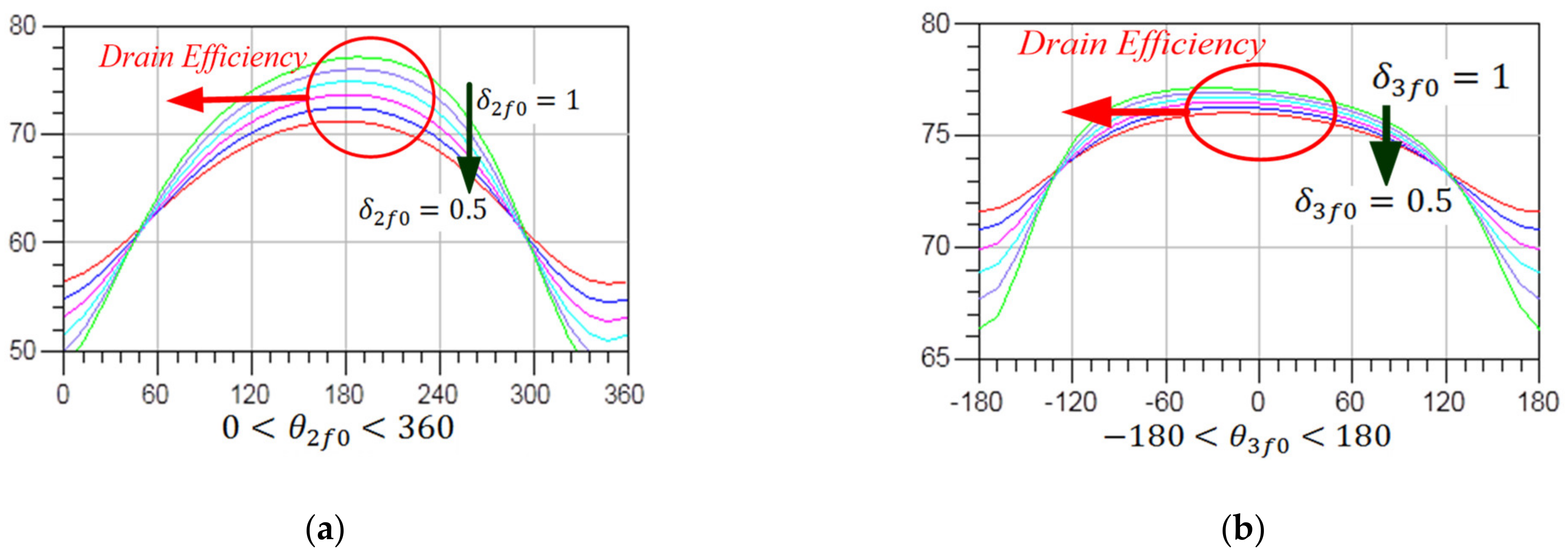
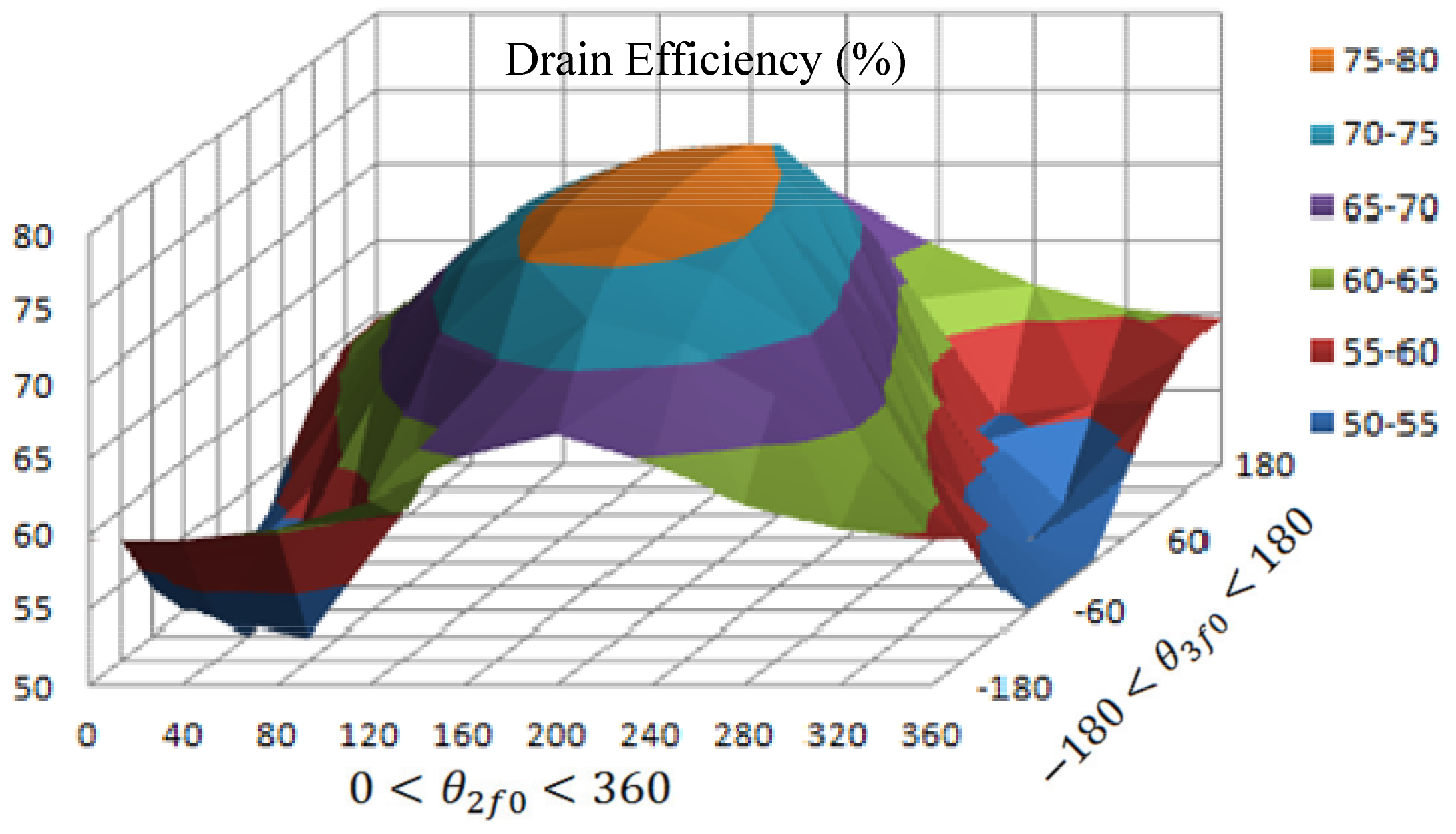
2. Design Space of Output Load Termination versus DE

As discussed in the introduction, it is difficult to realize nine precise impedances matching for the triple-band Class-F mode PA, since the output matching network will be so complex that it cannot be completed. So, the tradeoff between the DE and the output impedance should be considered. For example, if the efficiency can be maintained in a level, such as at 10% lower than the maximum efficiency of the standard Class-F mode, more realizations about the corresponding output impedances can be achieved, within a more flexible design region or “space”. This means that a simple matching network (instead of lots of stubs) may be possible for the realization of high efficiency within the multi-band.
For the standard Class-F mode operation, the fundamental impedance is chosen to be R o p t . For this specific transistor and the frequency of 2.1 GHz, R o p t = 40   Ohm , the second and third harmonic impedances are short and open, respectively. For a low-pass matching topology, the fundamental impedance can be broadband. The location of the second and third harmonic impedances will be mainly discussed in the following analysis.
First of all, the second harmonic impedance is tuned around the edge of the Smith chart, from short to open. Additionally, also considering the location in the inner Smith chart, as shown in Equation (1)
S 11 2 f 0 = δ 2 f 0 · c o s θ 2 f 0 + j · s i n θ 2 f 0
where 0 < θ 2 f 0 < 360   degrees , and 0.5 < δ 2 f 0 < 1 .
Then, the second harmonic impedance is,
Z 2 f 0 = 50 · 1 + S 11 2 f 0 / 1 S 11 2 f 0
Figure 2 a plots the DE for 0 < θ 2 f 0 < 360 degrees and 0.5 < δ 2 f 0 < 1 with a step of Δ δ 2 f 0 = 0.1 . For the δ 2 f 0 = 1 condition, if the second harmonic impedance is within 100 < θ 2 f 0 < 260 degrees, the efficiency can be maintained higher than 70%. However, if the magnitude of S 11 2 f 0 is smaller than 1, the high efficiency region is obviously decreased. For δ 2 f 0 = 0.5 , the maximum efficiency is only 71.8%, and the range of above 70% efficiency is within 130 < θ 2 f 0 < 210 degrees. So, in order to obtain a high efficiency, S 11 2 f 0 should be arranged across the edge of the Smith chart:
0.9 < δ 2 f 0 < 1
Using the same analyzing methodology, the third harmonic impedance is also studied. The third harmonic impedance is termed as:
S 11 3 f 0 = δ 3 f 0 · cos θ 3 f 0 + j · sin θ 3 f 0
where 180 < θ 3 f 0 < 180 degrees and 0.5 < δ 3 f 0 < 1 .
Figure 2b shows the results of DE versus the third harmonic termination of Equation (4). The high efficiency range of the third harmonic impedance is wider than the second harmonic impedance. In most conditions, the efficiency can be higher than 70%, which means that the second harmonics should be more restricted within short condition and the third harmonic can offer a more flexible range. In the same way, if the magnitude of S 11 3 f 0 declines, the high efficiency region is obviously decreased. So, in order to obtain a high efficiency, S 11 3 f 0 should be arranged across the edge of the Smith chart as the second harmonic impedance.
Based on our load termination matching experiences, by using the low-pass topology, the second and third harmonic impedances can be theoretically arranged within the edge of the Smith chart, but are difficult to locate in the specific points. This means that the condition of mag ( S 11 3 f 0 ) > 0.9 and mag ( S 11 2 f 0 ) > 0.9 can be achieved by utilizing a low-pass topology. Under this prerequisite, the phases’ influences of the second and third load terminations are considered together. As shown in Figure 3, the DE versus the phases of S 11 2 f 0 and S 11 3 f 0 is extracted. Assuming that the other parameters are fixed, the location of the reflection coefficient phases in Figure 3 can describe the corresponding efficiency clearly, which directly provides guidance for our matching design process.

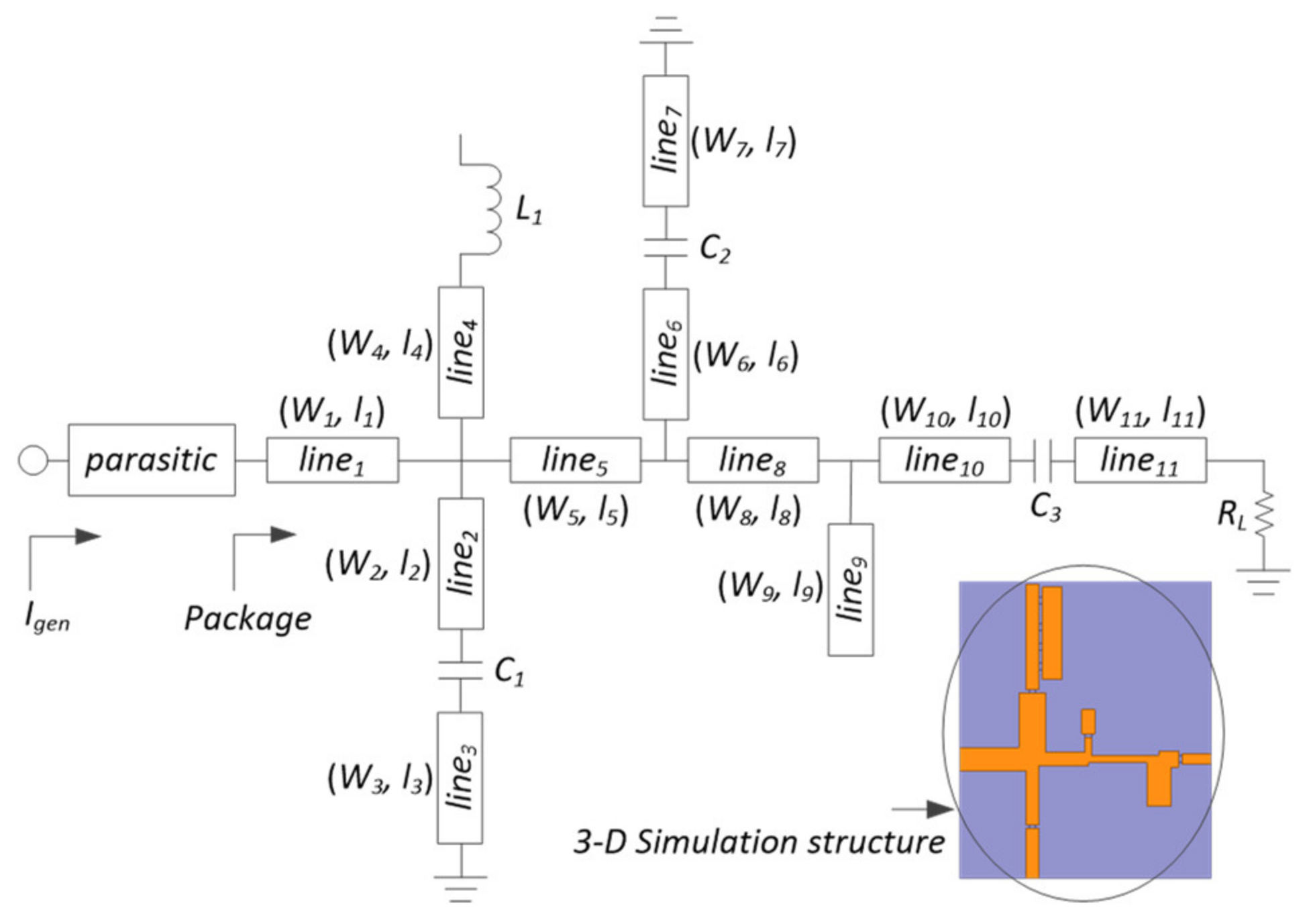
3. Triple-Band Output Load Termination Design

Based on the analyses in Section 2, one output matching topology for the triple-band PA realization will be discussed in this section. The three independent operation frequencies are f 1 = 1.52   GHz , f 2 = 2.1   GHz and f 3 = 2.492   GHz . The starting point of the design is the Class-F mode. The principle is utilizing the lowpass matching network to realize the fundamental, second and third harmonic impedances maintained within the high efficiency region at the three operation frequencies, while the frequencies between them are located in the lower efficiency area.
The output matching network is shown in Figure 4, with the dimensions summarized in Table 2. The substrate is Rogers RT5880 with a thickness of 0.254 mm and a relative permittivity of 2.2. The parasitic of the transistor is also included in our discussion. Electromagnetic simulation was performed in the output impedances matching. The final output matching result is shown in Figure 5, with the fundamental, the second and third harmonic impedances considered. The fundamental impedance is mainly located in the 40-Ohm region, with the second and third harmonic impedances located at the edge of the Smith chart, as a low-pass transition performance.
In order to realize the high-efficiency within the triple-band, the locations of the impendences were turned and optimized. Figure 5a plots the matching result in the high efficiency region. The location in the efficiency plot shows that the three matching results are all in the space of above 70%, which can guarantee high efficiencies in the desired triple-band. The horizontal ordinate is for 0 < θ 2 f 0 < 360 degrees, and Y-axis for 180 < θ 3 f 0 < 180 degrees.
The frequencies between the operation bands should also be considered to make sure that their locations are not in the high efficiency region. Figure 5b shows the locations of the output matching at frequencies between the triple-band: 1.7 GHz and 2.35 GHz. The second and third impedances of the two frequencies are located in the region where the efficiency is in the edge of 60%. This means that at these two frequencies, the efficiencies will be 10% lower than the required three operation bands. So, the obvious triple-band of efficiency can be explored.

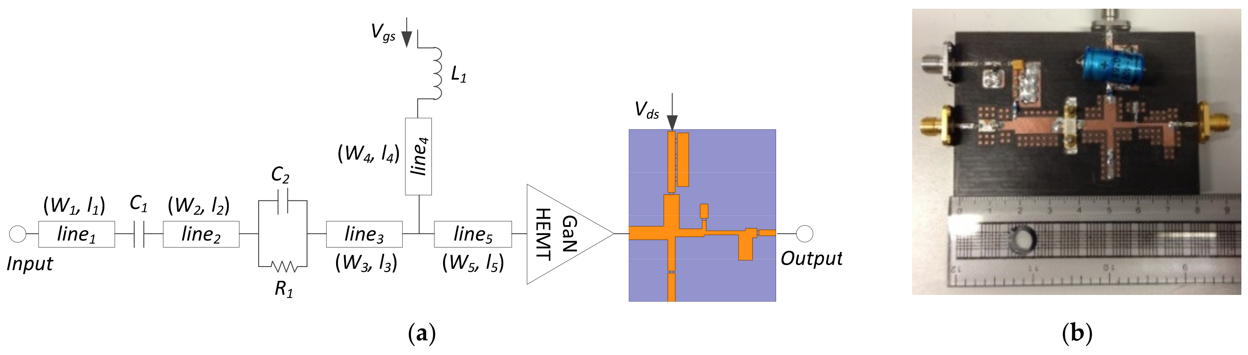
4. Triple-Band Efficiency-Optimized PA Realization

4.1. Continuous Wave Measurement

The circuit schematic and the photograph of the designed PA are shown in Figure 6, with the dimensions of input matching summarized in Table 3. The input matching network provides the gain optimization at the three fundamental frequencies simultaneously. The stability is also simulated and improved using a parallel of a resistor and a capacitor in the input branch. The simulated results and the continuous wave measurement results are summarized in Figure 7. Efficiency behavior in the triple-band is observed at 1.52 GHz, 2.1 GHz and 2.492 GHz, with the DE over 63%, 71% and 59%, respectively. It can be noted that the efficiency of the proposed PA has slight frequency-shift between the simulation and measurement results. This may be caused by the relative permittivity variation of the substrate used for fabrication. The agreement between the simulations and measurements in the first and second operation-band are good. However, the measured efficiency of the third band (2.492 GHz) is 16% lower than the simulation result. The reason is that the location of the impedances of 2.492 GHz is at the edge of the high-efficiency region and, therefore, is sensitive to the fabrication tolerance.

4.2. Linearity Measurement

The adjacent channel power ratio (ACPR) without any form of pre-distortion was measured across a range of drive powers for the realized PA. The input EDGE signal has 200 kHz channel bandwidth and 3.6 dB peak-to-average power ratio (PAPR).
The average efficiency, ACPR, and average output power are summarized in Table 4. The ACPR of −26 dBc with 40.4% average efficiency has been measured at 1.52 GHz, while the ACPR of −27 dBc and 42.56% average efficiency has been obtained at 2.1 GHz. At 2.492 GHz, the ACPR equals −26 dBc and the average efficiency is 36.99%.
In Table 5, the PA is compared with other wideband PAs in terms of operation bands and efficiencies. It can be seen that the proposed PA has a competitive efficiency in the desired triple-band compared to other broadband PAs in the latest literatures, but has a better rejection performance within the out-operation bands. The table also indicates that the efficiency of the proposed PA is better than the triple-band PAs of other works as well, in both continuous wave (CW) and modulated signal conditions.

5. Conclusions

The design methodology, implementation, and experimental results of a triple-band efficiency-optimized PA have been provided in this paper. Detailed discussions studied the design space of load terminations versus DE, mainly considering the second and third harmonic impedance regions. Then, a low-pass matching schematic was utilized as the output termination for the PA operating at 1.52 GHz, 2.1 GHz and 2.492 GHz. After the attentional optimization of the second and third harmonic impedances’ locations, high efficiencies within the desired triple-band were realized, achieving 63%, 71% and 59%, respectively, with an output power higher than 40 dBm. The results verify the concept about multi-band efficiency enhancement presented in this paper. The methodology can be realized for other transistors at other frequencies as well in future studies.

Author Contributions

Conceptualization, X.C. and A.Z.; Data curation, C.G.; Funding acquisition, J.L.; Investigation, F.Y. and H.Y.; Methodology, F.Y.; Project administration, Z.J.; Resources, Z.J.; Supervision, H.Y., J.L. and A.Z.; Validation, F.Y. and S.Y.; Writing—original draft, F.Y.; Writing—review & editing, C.G., S.Y. and X.C. All authors have read and agreed to the published version of the manuscript.

Funding

This research was funded by [Innovation support program of Shaanxi Province] grant number [S2020-ZC-XXXM-0071].

Institutional Review Board Statement

Not applicable.

Informed Consent Statement

Not applicable.

Data Availability Statement

Not applicable.

Conflicts of Interest

The authors declare no conflict of interest.

References

  1. Cripps, S. RF Power Amplifiers for Wireless Communications, 2nd ed.; Artech: London, UK, 2006. [Google Scholar]
  2. Tasker, P.J. Practical waveform engineering. IEEE Microw. Mag. 2009, 10, 65–76. [Google Scholar] [CrossRef]
  3. Nghe, C.T.; Maassen, D.; Nghiem, X.A.; Boeck, G. Ultra-wideband efficient linearized 10W GaN-HEMT power amplifier. In Proceedings of the 2017 IEEE International Symposium on Radio-Frequency Integration Technology (RFIT), Seoul, Korea, 30 August–1 September 2017; pp. 189–191. [Google Scholar] [CrossRef]
  4. Saxena, S.; Rawat, K.; Roblin, P. Continuous Class-B/J Power Amplifier Using a Nonlinear Embedding Technique. IEEE Trans. Circuits Syst. II Express Briefs 2017, 64, 837–841. [Google Scholar] [CrossRef]
  5. Zhuang, Y.; Fei, Z.; Chen, A.; Huang, Y.; Rabbi, K.; Zhou, J. Design of Multioctave High-Efficiency Power Amplifiers Using Stochastic Reduced Order Models. IEEE Trans. Microw. Theory Tech. 2018, 66, 1015–1023. [Google Scholar] [CrossRef] [Green Version]
  6. Jia, P.; You, F.; He, S.; Qian, X. A 0.25–1.25-GHz High-Efficiency Power Amplifier with Computer-Aided Design Based on Optimized Impedance Solution Continuum. IEEE Microw. Wirel. Compon. Lett. 2018, 28, 443–445. [Google Scholar] [CrossRef]
  7. Boroujeni, S.R.; Basaligheh, A.; Ituah, S.; Nezhad-Ahmadi, M.; Safavi-Naeini, S. A Broadband High-Efficiency Continuous Class-AB Power Amplifier for Millimeter-Wave 5G and SATCOM Phased-Array Transmitters. IEEE Trans. Microw. Theory Tech. 2020, 68, 3159–3171. [Google Scholar] [CrossRef]
  8. Quaglia, R.; Bell, J.J.; Cripps, S. New General Formulation and Experimental Verification of Harmonic Clipping Contours in High-Frequency Power Devices. IEEE Trans. Microw. Theory Tech. 2017, 65, 3903–3909. [Google Scholar] [CrossRef] [Green Version]
  9. Taleb-Alhagh Nia, H.; Nayyeri, V. A 0.85–5.4 GHz 25-W GaN Power Amplifier. IEEE Microw. Wirel. Compon. Lett. 2018, 28, 251–253. [Google Scholar] [CrossRef]
  10. Moreno Rubio, J.J.; Quaglia, R.; Baddeley, A.; Tasker, P.J.; Cripps, S.C. Design of a Broadband Power Amplifier Based on Power and Efficiency Contour Estimation. IEEE Microw. Wirel. Compon. Lett. 2020, 30, 772–774. [Google Scholar] [CrossRef]
  11. Qi, C.; Luo, Y.; Feng, X.; Dong, C. 1.6–2.6 GHz continuous Class-F power amplifier with gain and power-added efficiency flatness enhancement by negative feedback structure. Microw. Opt. Technol. Lett. 2019, 61, 1716–1722. [Google Scholar] [CrossRef]
  12. Ciccognani, W.; Colangeli, S.; Longhi, P.E.; Serino, A.; Giofré, R.; Pace, L.; Limiti, E. Broadband Amplifier Design Technique by Dissipative Matching Networks. IEEE Trans. Circuits Syst. I Regul. Pap. 2021, 68, 148–160. [Google Scholar] [CrossRef]
  13. Ghazizadeh, M.; Nayyeri, V. Design of a 50-W Power Amplifier with Two-Octave Bandwidth and High-Efficiency Using a Systematic Optimization Approach. IEEE Microw. Wirel. Compon. Lett. 2021, 31, 501–504. [Google Scholar] [CrossRef]
  14. Arnous, M.T.; Zhang, Z.; Barbin, S.E.; Boeck, G. A Novel Design Approach for Highly Efficient Multioctave Bandwidth GaN Power Amplifiers. IEEE Microw. Wirel. Compon. Lett. 2017, 27, 371–373. [Google Scholar] [CrossRef]
  15. De Mingo, J.; Carro, P.L.; García-Dúcar, P.; Valdovinos, A. Triple-Band Concurrent Reconfigurable Matching Network. IEEE Access 2021, 9, 96711–96721. [Google Scholar] [CrossRef]
  16. Lee, G.; Jung, J.; Song, J.-I. A Multiband Power Amplifier with a Reconfigurable Output-Matching Network for 10-MHz BW LTE Mobile Phone Applications. IEEE Trans. Circuits Syst. II Express Briefs 2015, 62, 558–562. [Google Scholar] [CrossRef]
  17. Singh, R.; Paramesh, J. A digitally-tuned triple-band transformer power combiner for CMOS power amplifiers. In Proceedings of the 2017 IEEE Radio Frequency Integrated Circuits Symposium (RFIC), Honolulu, HI, USA, 4–6 June 2017; pp. 332–335. [Google Scholar] [CrossRef]
  18. Cho, H.; Lee, M.; Park, C.; Park, J.Y. A Fully Integrated Switched Capacitor using Low Temperature and Wet Release Process for Reconfigurable CMOS Triple-band Power Amplifier. In Proceedings of the 2019 IEEE Asia-Pacific Microwave Conference (APMC), Singapore, 10–13 December 2019; pp. 1467–1469. [Google Scholar] [CrossRef]
  19. Son, H.S.; Kim, W.Y.; Jang, J.Y.; Oh, I.Y.; Park, C.S. A Triple-Band CMOS Class-E Power Amplifier for WCDMA/LTE Applications. In Proceedings of the 2013 IEEE Asia-Pacific Microwave Conference (APMC), Seoul, Korea, 5–8 November 2013; pp. 441–443. [Google Scholar] [CrossRef]
  20. Arabi, E.; Enrico de Falco, P.; Birchall, J.; Morris, K.A.; Beach, M. Design of a triple-band power amplifier using a genetic algorithm and the continuous mode method. In Proceedings of the 2017 IEEE Topical Conference on RF/Microwave Power Amplifiers for Radio and Wireless Applications (PAWR), Phoenix, AZ, USA, 15–18 January 2017; pp. 48–51. [Google Scholar] [CrossRef] [Green Version]
Figure 1. (a) Waveform and (b) load-line of the Class-F using 10-W idealized and realistic GaN HEMT at 2.1 GHz.
Electronics 11 00310 g001
Figure 2. Output load termination design space versus DE at 2.1 GHz: (a) Second harmonic impedance and (b) third harmonic impedance.
Electronics 11 00310 g002
Figure 3. Second and third harmonic impedances design space versus DE for the low-pass topology with the fundamental frequency of 2.1 GHz.
Electronics 11 00310 g003
Figure 4. Schematic of the output matching network.
Electronics 11 00310 g004
Figure 5. Output load terminations’ locations in the corresponding efficiency plots: (a) in the three operation bands and (b) between the three operation bands.
Electronics 11 00310 g005
Figure 6. Proposed PA: (a) schematic and (b) fabricated photograph.
Electronics 11 00310 g006
Figure 7. Simulation and measurement results of the proposed PA: DE, output power and gain.
Electronics 11 00310 g007
Table 1. Idealized and realistic transistor performances of Class-F mode at 2.1 GHz.
Output Power (dBm)DE (%)
Idealized4290.6
Realistic41.279.2
Table 2. Dimensions of the output matching network.
l 1 w 1 l 2 w 2 l 3 w 3 l 4
11 mm3.5 mm10 mm2 mm6.5 mm2 mm10 mm
w 4 l 5 w 5 l 6 w 6 l 7 w 7
4 mm8.5 mm2 mm3.3 mm1 mm3.2 mm2 mm
l 8 w 8 l 9 w 9 l 10 w 10 l 11
10.7 mm1.1 mm7.15 mm3.6 mm2.94 mm2.5 mm6 mm
w 11 L 1 C 1 C 2 C 3 R L
1.54 mm15 nH51 pf51 pf51 pF50 Ohm
Table 3. Dimensions of the input matching network.
l 1 w 1 l 2 w 2 l 3 w 3 l 4
5 mm1.54 mm5.5 mm4 mm5.75 mm2.9 mm5 mm
w 4 l 5 w 5 L 1 C 1 C 2 R 1
1.5 mm15.85 mm5.4 mm120 nH51 pF51 pF10 Ohm
Table 4. Linearity measurement results.
Freq. (GHz)ACP1_L (dBc)ACP1_H (dBc)Pout (dBm)Pout (W)DE (%)
1.52−26.3−26.135.943.9340.40
2.1−27.3−2735.843.8442.56
2.492−26.5−2635.743.7536.99
Table 5. Comparison with recently reported works.
Ref.Operation Bands (GHz)DE at Operation Bands (%)Pout (dBm)Gain (dB)Signal Mode
[10]Broadband: 0.45–3.454~70.4>418~10.5CW
[13]Broadband: 0.8–3.257~71>46.89.5~13.1CW
[18]0.8/1.9/2.340/45/3728/29/6/26.5/CW
[19]1.8/1.9/2.631/34.5/29.227.8/28.1/27.4/CW
[20]0.75/1.75/2.3570/60/5841/40/4012/11/10CW
This work1.52/2.1/2.49263/71/5941.6/41.3/4011.5/12/10CW
40.4/42.56/36.9935.94/35.84/35.74>10EDGE
Publisher’s Note: MDPI stays neutral with regard to jurisdictional claims in published maps and institutional affiliations.

