1. Introduction
The huge growth of ICT, electromobility, renewables, industrial technologies, data centers and data storage increases the daily demands on the electricity supply. In connection with the increase in the level of electronics in all consumer and industrial sectors, alongside the demand for electricity, the phenomenon concerning its quality is important. At present, due to the availability of electricity, the 1-phase or three-phase distribution network distribution is mainly used. However, most electrical equipment requires one-way distribution, which must be adapted accordingly. For this reason, most devices are equipped with an AC/DC converter that allows the devices to connect directly to the network. High efficiency and power factor are important features of these converters [
1,
2,
3,
4,
5].
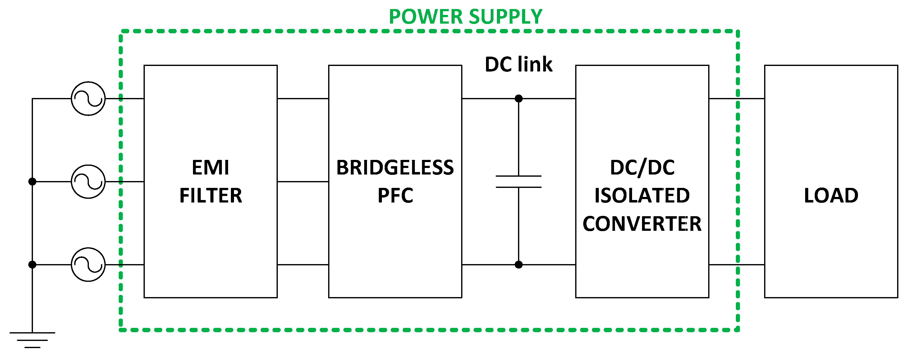
If we focus on the power supply concept of most industrial or consumer devices, it can be block-arranged in the configuration shown in
Figure 1. In general, the description of this structure can be divided into a filter, a rectifier and a power factor correction circuit also providing a constant voltage in the DC circuit. After the PFC converters, there are then additional DC/DC stages providing the required voltage levels for the connected devices. However, the above-mentioned power supply concept (
Figure 1) currently represents a solution that has been known for decades. However, it should be noted that the research of circuit topologies of individual stages of the mentioned concept is constantly improving and being perfected. Our discussion concerns a circuit solution, but also a technological one, specifically in terms of the production of semiconductor elements or magnetic components [
6,
7,
8,
9].
If we now focus specifically on circuit solutions, we will deal in more detail with the possibilities of solving the input element, i.e., the PFC converter. For the past few decades, various bridgeless boost PFC converters have been proposed. Many topologies based on basic bridgeless PFC have a common mode (CM) noise problem due to the floating input voltage. Dual-boost bridgeless PFC with the returned diode can avoid the CM noise problem. Totem-pole bridgeless boost PFC has a smaller CM noise than other bridgeless topologies, because the input is clamped to the output by diodes during each half-line cycle. Additionally, it has a small number of circuit elements. However, due to the poor reverse recovery characteristic of intrinsic body diode in general MOSFET switch, the use of the totem-pole bridgeless boost PFC has been limited to continuous conduction mode (CCM) operations. Depending on the application, devices might be rated from a few Watts to megawatts of power. Standard IEC 61000-3-2 defines the harmonic limits for the equipment input current up to 16 A per phase, i.e., for up to 10 kW of power for a three-phase equipment. When solving the main circuit of 3-phase connections of PFC converters, we also come across various configurations [
10,
11]. A long-known solution is the standard PFC boost connection in cooperation with a 3-phase rectifier. A potential improvement in the properties of this standard PFC converter lies in the so-called interleaved solution. With the advent of single-phase bridgeless topologies, a similar phenomenon can be registered in three-phase connections. The most widespread and most used solution is the so-called 6-switch 3-phase PFC converter in bridge connection, thanks to the development and advent of new generations of SiC transistors [
12,
13,
14,
15,
16,
17,
18].
Considering the technological development of wide-bandgap components, it can be noted that SiC technology has held a relatively stable place in terms of the choice of semiconductor components in high-performance electronic systems. Manufacturers have a wide portfolio of these elements, while the differences in electrical properties are mainly due to technological know-how [
19,
20,
21].
In this paper, the main research focus is on the analysis of the operational performance of selected SiC transistors within the main circuit of a 6-switch 3-phase PFC converter. Parameters of transistors are similar, including type of the package, so here we conduct an evaluation of competing products from different manufacturers. Similar studies have not been conducted, while the evaluation of the performance between Si, SiC and GaN type semiconductors has been provided [
22,
23,
24,
25]. The requirements for driving power as well as for the evaluation of loss ratios of selected transistor structures are evaluated. At the end of the article, attention is paid to the analysis of the efficiency of the proposed PFC converter, for different variants of the transistors used.
2. 3-Phase Bridgeless PFC Converter
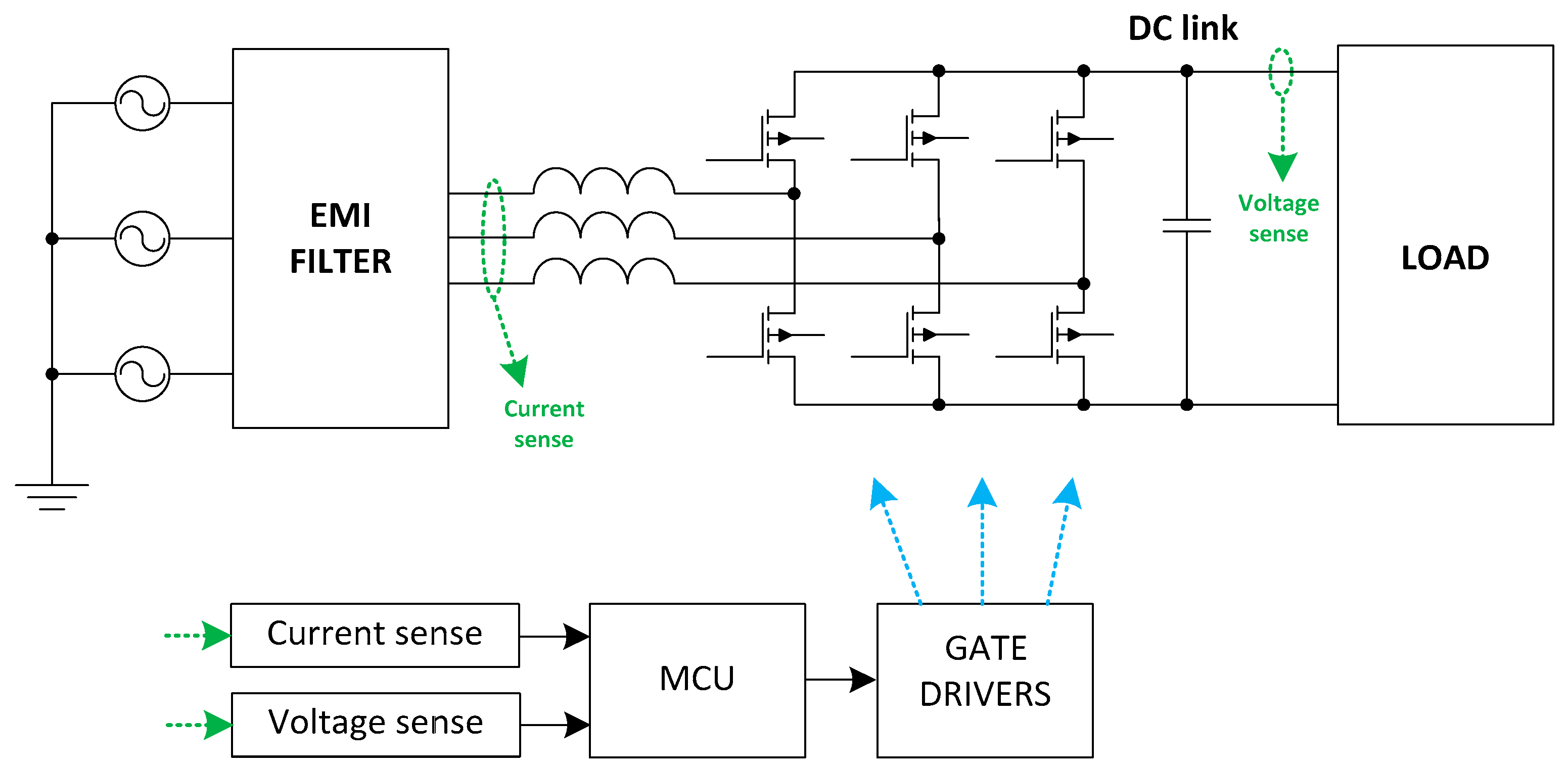
A conventional 3-phase 6-switch PFC converter is depicted on
Figure 2. The circuit schematic here also consists of additional circuits such as:
EMI line filter, which is responsible for EMC compatibility relates to connected devices on the DC side of the converter.
Damping circuit composed of shunt resistors and compensation capacitors connected to the EMI line filter.
PFC boost inductor also forming part of the sinusoidal LCL filter together with previously described components.
Main circuit of 6-switch 3-phase PFC converter together with DC-link filtering capacitor.
Sensing devices for monitoring the values of voltages and currents withing the main circuit.
Control unit with Gate drive circuits.
Nominal operational input/output parameters of PFC converter subjected to evaluation of SiC transistors performance are as follows:
For above mentioned parameters, the required main circuit components have been calculated and selected as well. Here, we are discussing about input PFC inductors, and output capacitor filters.
The physical prototype of experimental sample of proposed PFC converter is shown on
Figure 3.
Driver Selection and Circuit Configuration
The UCC21521 is an isolated dual-channel gate driver with a 4-A source and 6-A sink peak current (
Figure 4). It is designed to drive power MOSFETs, IGBTs, and SiC MOSFETs up to 5-MHz with an optimal propagation delay and pulse-width distortion. It uses a 5.7 kV isolation capacitive driver, which is one of the conditional features of a driving circuit for the defined operational conditions of the proposed 3-phase PFC converter.
Figure 5 presents the circuit schematic of the output stage of the utilized driver for one leg/phase of the PFC converter. The additional circuitry connected to the pins VDDA, OUTA, VSSA and VDDB, OUTB and VSSB, respectively, is responsible for formation of the −3V up to +13V of the driving V
GS signal. The required voltage supply for the driver ICs is realized with the use of independent DC/DC galvanically isolated converters.
Figure 6 displays a physical prototype of the driving board for the proposed 3-phase PFC converter, listing the identification of the main operational parts of this driving board.
3. Configuration of Experimental Set-Up
The procedure for testing was performed under laboratory conditions (
Figure 7). Experimental measurements were performed with calibrated laboratory equipment from renowned manufacturers such as Tektronix, Elektro-Automatik, Zimmer and Chroma. A block diagram of the experimental test-bench is shown on
Figure 8.
The 3-phase programmable AC source Chroma 61,505 was used as an input source of the tested power converter. The change of the output power was performed by electronic load EA-ELR 91000-30 3U. Measurements related to the efficiency evaluation were obtained via the evaluation of effective values of the input (Zimmer LMG 500) and output variables, i.e., voltages and currents. This was performed by Fluke 45 (output ammeter) and Agilent 34401A (output voltmeter). The base accuracy of LMG 500 is 0.015% of the reading and has a 0.01% range, thus the total measuring error is 0.025%. This allows for a correct measurement of the very low currents in the 32A range. Agilent 34,401 has basic accuracy on the level of 0.0035%, while Fluke 45 reaches an accuracy 0.2% of the measurements within the DC current range of 10 A.
Time waveforms were recorded with the use of the oscilloscope Textronix MDO3034 equipped with voltage and current probes from Tektronix (TM503 + A6302, P5200A). List of used laboratory equipment is given in
Table 1.
4. Selection Criterions on Power Transistor
The right selection of semiconductor devices in power converters is an essential design issue for proper operation. Nowadays, there are many varieties to choose the right semiconductor technology from, so as to obtain optimal characteristic parameters for target application. The design of the power converter is a complex process, but some widely used design techniques are commonly known. Within the first design steps, it is necessary to evaluate all aspects of the final electronic device, such as the expected performance, voltages, currents and, to assess the economical and size aspects to choose optimal semiconductor technology. Furthermore, the design process starts with the selection of optimal semiconductor technology, which is necessary for the requested parameters of converter system.
Since the designed converter will be supplied with middle type voltages AC 3 × 230 V and the output of the converter is 400–800 Vdc with a middle range of power output (3 kW), the semiconductor technologies from right side of flowchart seems to be optimal for this design (
Figure 9). Additional PFC converter properties are related to reliability and favourable power density, while the low-cost aspects should be considered [
26,
27]. Due to flowchart and assumed requirements, the SiC semiconductor technology is selected as the proposed PFC converter. This technology offers very good static and dynamic parameters since middle and high switching frequencies can be used. Overall, a power converter design equipped with SiC technology will offer excellent parameters with preservation of small dimensions, small magnetics sizes and friendly economical aspects.
Looking at the commercially available SiC power transistor structures, the selection criterion is determined by the target application of proposed PFC converter. This is related to voltage blocking capability, while proposed PFC converter is expected to source 800 Vdc at DC link side. Therefore, 1.2 kV transistor types have been selected from several manufacturers.
Table 2 lists selected types together with the main electrical parameters of the transistors. Because this study is not a presentation or advertisement for specific type of transistor, or manufacturer, the type designations are not provided.
As can be seen in the table, alternatives with lower and higher current capabilities have been selected. Both alternatives are suitable if the nominal parameters of the proposed PFC converter are considered. However, it must be noted here that the current rating capability is in direct relationship to the value of resistance of the conduction channel. This is reflected in the values of conduction losses. On the other side, transistors with low RDS(ON) are specified with a higher value of output capacitance COSS, for which the value is the main parameter affecting switching losses. Therefore, these variations are experimentally evaluated in the way of evaluation of efficiency performance of the PFC converter, so as to assess which element of the loss is most dominant.
5. Experimental Measurement Results
During experimental testing, several key operational performances were evaluated during transistors operation. At first, the gate-source voltage transient during the turn-on process was observed. From the dynamic point of view, the switching times were evaluated, i.e., the fall and rise time were of the nominal operational conditions proposed for the PFC converter. Consequently, requirements on the driver, i.e., driving current and power for individual transistors was evaluated. Finally, the efficiency performance of the PFC converter operated under nominal conditions was also measured.
5.1. Dynamic Performance Evaluation
The first measurement of the dynamic transients related to the gate-source driving voltage was realized for transistor SiC v1. The evaluation was realized using time waveforms recorded by oscilloscope Tektronix MDO3034, while the rise time from a non-conducting state (0 V) to a fully opened transistor (10–11 V) was measured. The recorded time waveforms for selected transistor structures are shown on
Figure 10,
Figure 11,
Figure 12 and
Figure 13. Graphical interpretation of received results are consequently provided in
Figure 14. From the measurements it can be seen that the fastest turn-on transient can be observed for the transistors with the lowest values of input capacitances, i.e., for SiC v1 and SiC v4. On the other side, better performance for SiC v3 was observed compared to SiC v2, where even the C
ISS of SiC v2 is smaller, but the reason here of the worse dynamic performance is the higher demand on the Q
G of SiC v2.
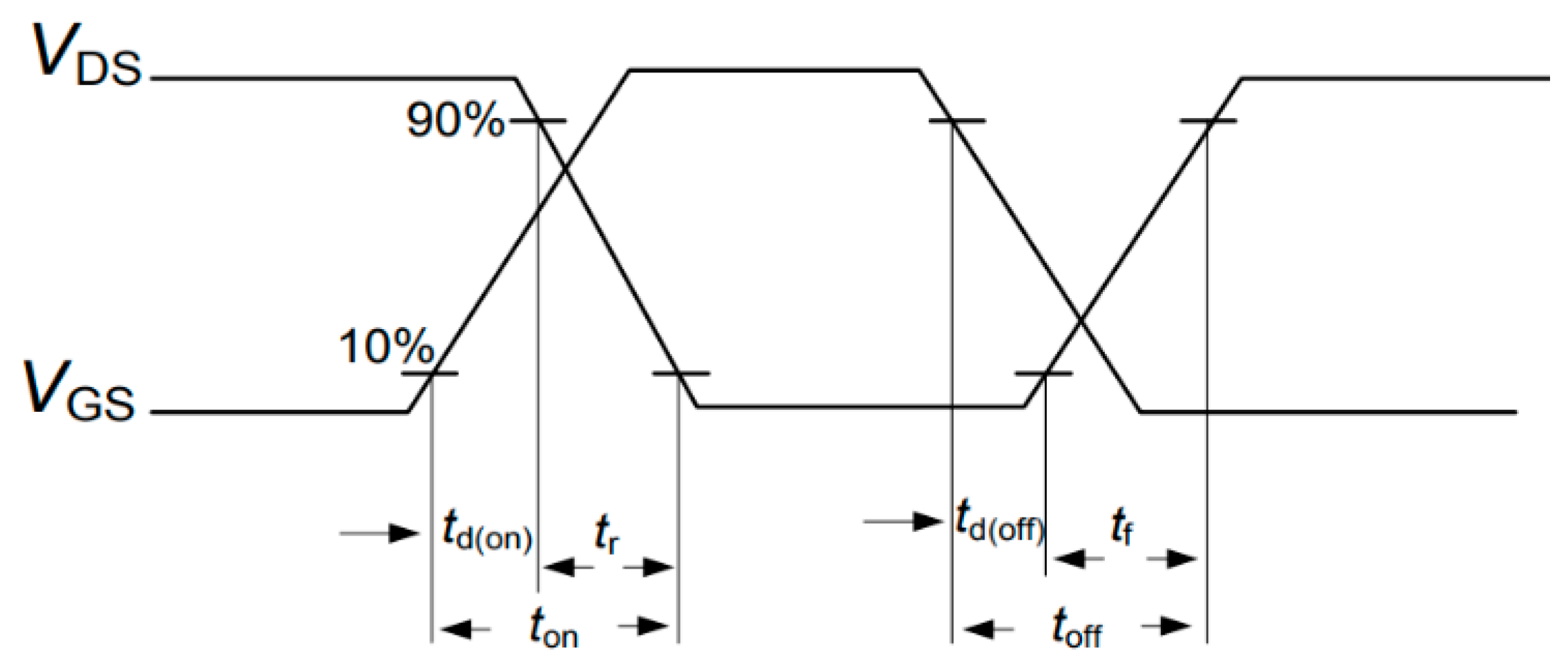
The second evaluation of the dynamic performance of selected SiC transistors was related to the evaluation of turn-on and turn-off times during switching operation. These measurements were performed similarly to the instructions provided by the transistor manufacturers (
Figure 15). Here, it must be stated that t
on = t
d(on) + t
r, and t
off = t
d(off) + t
f, while measurements identify total turn-on and turn-off times without identifying delays or rise/fall times.
The values of the switching time transients is dependent on the values of operational conditions of the converter/transistor itself. Therefore, the evaluation of switching times was realized for two values of operational voltage, i.e., 400 Vdc and 800 Vdc at the DC link of converter (
Figure 2). The results received from the experimental measurements are listed in
Figure 16 for both turn-on and turn-off switching transients. For both values of voltage DC-link, the power delivery of the converter was set to 3 kW.
As was observed from measurements, and based on description given in previous chapters, the choice of the right semiconductor device is a complex decision-making process, and many parameters must be considered.
Figure 17 summarizes the achieved results, while the dependencies of some static and dynamic parameters were graphically interpreted to simplify the selection criterions on power transistor for their specific design.
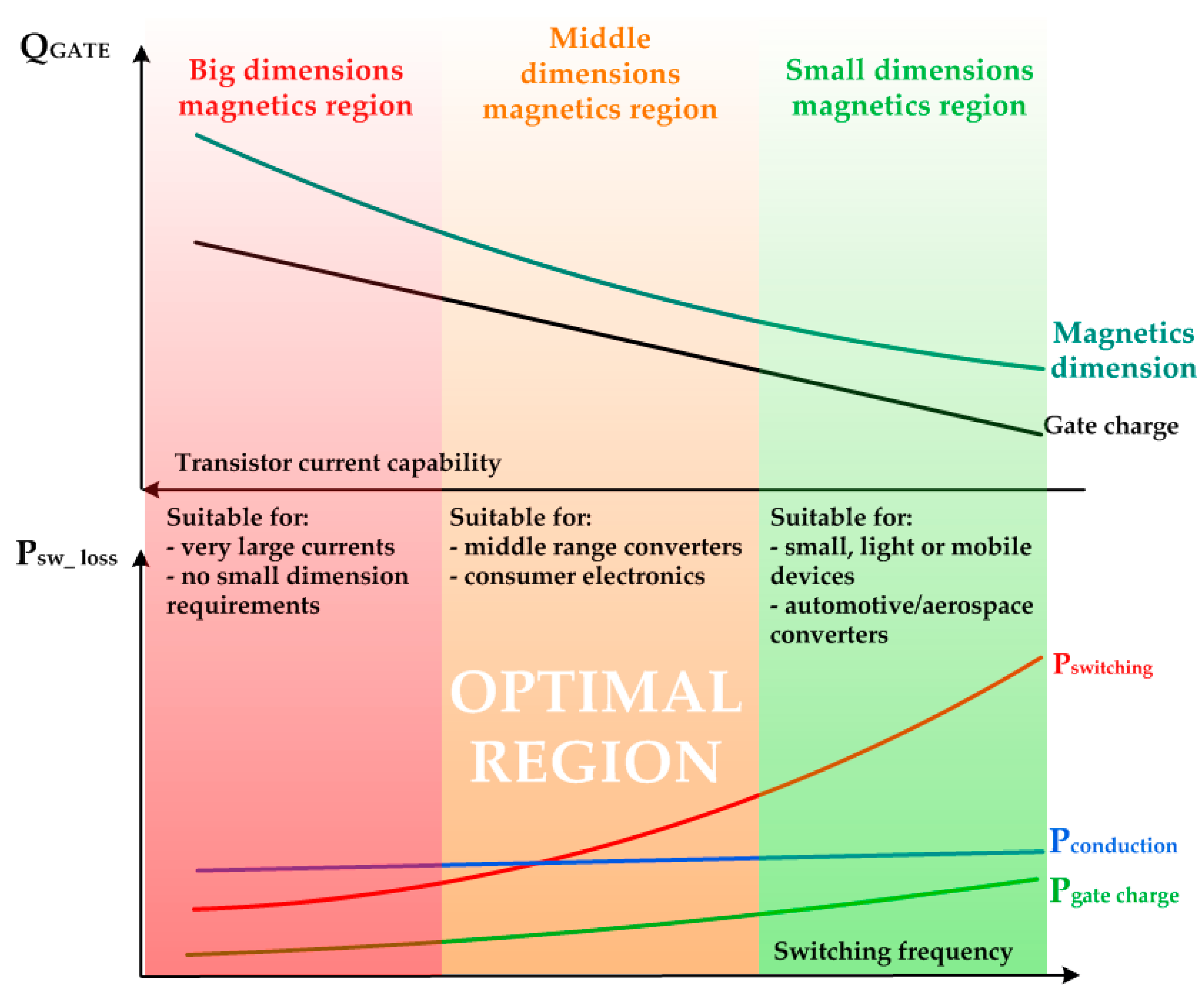
With an increase in the switching frequency, the parasitic capacitances and dynamic parameters of the semiconductor devices worsened, thus it results in an increase in switching losses. On the other side, an increase in switching frequency has a positive effect on the reduction of the magnetics size, but the opposite effect is the increase in magnetisation losses in magnetic material due to a higher frequency. Due to these facts, the high switching frequency with low magnetics sizes are used with advantages in small power converters with low output-power delivery.
If the requirement of heavy power converter comes with high power and current values, the semiconductor switches with low conduction parasitics, together with a combination of low switching frequency, are used to achieve high efficiency. However, the consequence is that magnetic component should also be big and heavy.
For the designed PFC converter, the selection of proper components is a compromise between optimal values of static parameters (affects conduction losses) and parasitic capacitances (affect the switching losses). As is shown in
Figure 17, the design constraints of a PFC converter are located within the optimal region defined by the cross section of static and dynamic losses.
5.2. Evaluation of the Power Consumption and Efficiency Performance
As was mentioned within the introduction of this study, efficiency, or power consumption is one of the most important qualitative indicators of switched-mode power supplies. Therefore, at this point, an evaluation of the requirements on the driving power during turn-on transient and a measurement of the gate-sink current were performed (
Figure 18). Based on the values from
Table 2, it can be expected that the transistor with the highest input capacitance would have the highest demands on driving power. This is also confirmed by the measurements, presented in the graphical comparison in
Figure 18.
An evaluation of the efficiency performance was realized under operational conditions, with the DC link voltage initially set to 400 Vdc and consequently to 800 Vdc. For both cases, the output power was maintained at 3 kW (
Table 3).
The graphical interpretations of the results of the efficiency are shown on
Figure 19. From the presented values, it is seen that for transistors V2 and V3, the difference of the efficiency for 400 Vdc and 800 Vdc of output voltage is negligible. This difference varies on the level of the measuring error of the laboratory equipment. On the other side, transistors V1 and V4 show a higher difference when comparing the situation for 400 Vdc and 800 Vdc. It is clear that better efficiency is achieved for a higher output voltage value. This fact could be affected by the parasitic capacities’ nonlinear voltage dependency, while for lower voltages the higher value exists, thus decreasing the dynamic performance of the transistor structure.
6. Discussion
Based on the experimental measurements, it is useful to identify whether the parameters for transistor characterization and their associated performances are in conflict with each other. For this purpose, a correlation analysis was performed [
28], while the following characteristic parameters were evaluated:
Total gate charge—QG(tot)
Fall and rise time of gate voltage—trise, tfall
Input and output capacitance—CISS, COSS
Efficiency—η
Based on correlation analysis of the selected parameters, for which the values were selected based on
Table 2, it can be concluded that there are very statistically significant relationships between them. The following results were observed:
As the overall gate charge of the transistor increases, its input and output capacities increase modestly, but its resistance of the conduction channel decreases.
The decreasing resistance of the transistor increases the efficiency of the system.
The rise and fall time are related, which is logical because a slower transistor has longer and better shape of driving signal.
With increasing input capacitance, the transistor also has an increased output capacitance, and a very strong correlation was found in that if the input capacitance increases with the transistor, the resistance of the conduction channel decreases.
The most significant correlations are highlighted in
Table 4.
7. Conclusions
In this study, the investigation of the influence of power-transistor selection on the operational efficiency of PFC was evaluated, together with an experimental analysis of the dynamic performance and driving requirements of selected transistor structures. For the designed PFC converter, the selection of proper components is a compromise between optimal values of static parameters (affects conduction losses) and parasitic capacitances (affect the switching losses). When selecting the appropriate type of transistor for a three-phase PFC, four types from three manufacturers of SiC transistors were selected. Individual transistors differ mainly in the value of drain current, while high current (app. 90 A) and middle current capability (app. 30A) transistors were evaluated. This essential property has a direct influence on the other performance, i.e., on the dynamic behaviour and gate-drive requirements. Based on these differences, the evaluation of operational performance of individual transistors has been realized, while the impact of this was reflected in the efficiency performance of the proposed PFC converter. From the measurements, we observed that the fastest turn-on transient is valid for transistors with the lowest values of input capacitances. On the other side, even CISS is hypothetically low, and the worst dynamic performance is reached when a higher demand on the QG is simultaneously required.
The efficiencies at a DC link voltage of 400V and 800V with 3 kW of power delivery were compared. The efficiencies ranged from around 98.5 to 99.6 percent according to the transistor manufacturer and measurements. The worst dynamic performance of the selected types was observed for the transistor with the highest required gate charge. On the other side, this transistor represents a robust solution because of the low RDS(ON) and thus, the high current capability. This was reflected in particularly low conduction losses because the total efficiency of the evaluated PFC with this type of transistor reached overall comparable results to the much faster types selected.
Author Contributions
Conceptualization, methodology, writing—original draft preparation, funding acquisition, M.F., hardware, validation, investigation J.M. and B.H. All authors have read and agreed to the published version of the manuscript.
Funding
This research was funded by National Grant Agency Vega, grant number 1/0063/21 and by National Grant Agency APVV for project funding APVV-20-500.
Acknowledgments
The authors wish to thank for the support to the National Grant Agency Vega, grant number 1/0063/21 and by National Grant Agency APVV for project funding APVV-20-500.
Conflicts of Interest
The authors declare no conflict of interest.
References
- Park, M.; Baek, J.; Han, J.; Lim, C.; Moon, G. ZVS Interleaved Totem-pole Bridgeless PFC Converter with Phase-shifting Control. In Proceedings of the 2018 International Power Electronics Conference (IPEC-Niigata 2018-ECCE Asia), Niigata, Japan, 20–24 May 2018; pp. 3533–3537. [Google Scholar] [CrossRef]
- Prahallad, P.C.; Bauer, P.; Schellekens, J. Cost analysis of three phase PFCs and selection of the cost-effective PFC for a specified power level. In Proceedings of the 2019 11th International Symposium on Advanced Topics in Electrical Engineering (ATEE), Bucharest, Romania, 28–30 March 2019; pp. 1–6. [Google Scholar] [CrossRef]
- Krishna, R.A.; Suresh, L.P. A brief review on multi level inverter topologies. In Proceedings of the 2016 International Conference on Circuit, Power and Computing Technologies (ICCPCT), Nagercoil, India, 18–19 March 2016; pp. 1–6. [Google Scholar] [CrossRef]
- Hassan, A.; Yang, X.; Chen, W.; Houran, M.A. A State of the Art of the Multilevel Inverters with Reduced Count Components. Electronics 2020, 9, 1924. [Google Scholar] [CrossRef]
- Hruska, K.; Kindl, V.; Pechanek, R. Design of a high-speed permanent magnet synchronous motor for electric kart. Electr. Eng. 2017, 99, 1141–1150. [Google Scholar] [CrossRef]
- Galád, M.; Špánik, P.; Cacciato, M.; Nobile, G. Comparison of common and combined state of charge estimation methods for VRLA batteries. In Proceedings of the 2016 ELEKTRO, Strbske Pleso, Slovakia, 16–18 May 2016; pp. 220–225. [Google Scholar] [CrossRef]
- Zaskalicky, P. Complex fourier series analysis of a three-phase induction motor supplied by a three-phase inverter with PWM output voltage control. In Proceedings of the 2014 16th International Power Electronics and Motion Control Conference and Exposition, Antalya, Turkey, 21–24 September 2014; pp. 1183–1188. [Google Scholar] [CrossRef]
- Nobile, G.; Scelba, G.; Cacciato, M.; Scarcella, G. Losses Minimization Control for an Integrated Multidrive Topology Devoted to Hybrid Electric Vehicles. IEEE Trans. Ind. Electron. 2019, 66, 8345–8360. [Google Scholar] [CrossRef]
- Magura, D.; Fedak, V.; Kyslan, K. Modeling and analysis of multi-motor drive properties in a web processing continuous line. In Proceedings of the 16th Conference on Modelling of Mechanical and Mechatronic Systems (MMaMS), High Tatras, Slovakia, 25–27 November 2014; Volume 96, pp. 281–288. [Google Scholar]
- Cacciato, M.; Caricchi, F.; Giuhlii, F.; Santini, E. A critical evaluation and design of bi-directional DC/DC converters for super-capacitors interfacing in fuel cell applications. In Proceedings of the Conference Record of the 2004 IEEE Industry Applications Conference, 2004. 39th IAS Annual Meeting, Seattle, WA, USA, 3–7 October 2004; Volume 2, pp. 1127–1133. [Google Scholar] [CrossRef]
- Sallan, J.; Villa, J.L.; Llombart, A.; Sanz, J.F. Optimal Design of ICPT Systems Applied to Electric Vehicle Battery Charge. IEEE Trans. Ind. Electron. 2009, 56, 2140–2149. [Google Scholar] [CrossRef]
- Kindl, V.; Hruska, K.; Sobra, J.; Byrtus, M. Effect of induction machine’s load and rotor eccentricity on space harmonics in the air gap magnetic flux density. In Proceedings of the 16th International Conference on Mechatronics—Mechatronika 2014, Brno, Czech Republic, 3–5 December 2014; pp. 463–468. [Google Scholar] [CrossRef]
- Ismeal, G.A.; Kyslan, K.; Fedak, V. DC Motor Identification Based on Recurrent Neural Networks. In Proceedings of the 16th International Conference on Mechatronics (Mechatronika), Brno, Czech Republic, 3–5 December 2014; pp. 701–705. [Google Scholar]
- Musznicki, P.; Rucinski, M.; Turzynski, M.; Abramik, S. Prediction of ringing frequencies in DC-DC boost converter. In Proceedings of the 2016 International Symposium on Electromagnetic Compatibility—EMC EUROPE, Wroclaw, Poland, 5–9 September 2016; pp. 672–675. [Google Scholar] [CrossRef]
- Dobrucky, B.; Kascak, S.; Prazenica, M.; Jarabicova, M. Improving Efficiency of Hybrid Electric Vehicle Using Matrix Converters. Elektron. Elektrotechnika 2019, 25, 29–35. [Google Scholar] [CrossRef] [Green Version]
- Kolar, J.W.; Friedli, T. The essence of three-phase PFC rectifier systems. In Proceedings of the 2011 IEEE 33rd International Telecommunications Energy Conference (INTELEC), Amsterdam, The Netherlands, 9–13 October 2011; pp. 1–27. [Google Scholar] [CrossRef]
- Azazi, H.Z.; Mahmoud, S.A.; Shokralla, S.S. Review of passive and active circuits for power factor correction in single phase, low power AC-DC converters. In Proceedings of the 14th International Middle East Power Systems Conference (MEPCON’10), Shebin El-Kom, Egypt, 19–21 December 2010; Electrical Engineering Department, Faculty of Engineering, Menoufiya University: Shebin El-Kom, Egypt, 2010. [Google Scholar]
- Mohan, N.; Undeland, T.; Robbins, W. Power Electronics. ISBN 0-471-58408-8. Available online: http://fuuu.be/polytech/LANGH300/LED/1995_BOOK_Mohan_820p_Power_Electronics_2nd.pdf (accessed on 15 December 2021).
- Liu, B.; Ren, R.; Jones, E.; Wang, F.; Costinett, D.; Zhang, Z. A compensation scheme to reduce input current distortion in a GaN based 450 kHz three-phase Vienna type PFC. In Proceedings of the 2016 IEEE Energy Conversion Congress and Exposition (ECCE), Milwaukee, WI, USA, 18–22 September 2016; pp. 1–7. [Google Scholar] [CrossRef]
- Zhu, H.; Li, B.; Wang, K.; Yang, X. Common-Mode EMI Modeling and Analysis for GaN-Based Full-Bridge CRM PFC under Unipolar PWM Scheme. In Proceedings of the 2020 IEEE Workshop on Wide Bandgap Power Devices and Applications in Asia (WiPDA Asia), Suita, Japan, 23–25 September 2020; pp. 1–5. [Google Scholar] [CrossRef]
- Do, N.-N.; Huang, B.-S.; Phan, N.-T.; Nguyen, T.-T.; Wu, J.-H.; Liu, Y.-C.; Chiu, H.-J. Design and Implementation of a Control Method for GaN-Based Totem-Pole Boost-Type PFC Rectifier in Energy Storage Systems. Energies 2020, 13, 6297. [Google Scholar] [CrossRef]
- Tiwari, S.; Basu, S.; Undeland, T.M.; Midtgård, O. Efficiency and Conducted EMI Evaluation of a Single-Phase Power Factor Correction Boost Converter Using State-of-the-Art SiC Mosfet and SiC Diode. IEEE Trans. Ind. Appl. 2019, 55, 7745–7756. [Google Scholar] [CrossRef]
- Chen, W.; Zhang, C.; Qu, K.; Hu, B.; Chen, J.; Wang, J. A New Hybrid Si/SiC CCM Totem Pole Bridgeless PFC Design Towards Optimal Performance and Cost Tradeoff. In Proceedings of the 2021 IEEE Energy Conversion Congress and Exposition (ECCE), Vancouver, BC, Canada, 10–14 October 2021; pp. 2203–2207. [Google Scholar] [CrossRef]
- Jang, J.; Pidaparthy, S.K.; Lee, S.; Choi, B. Performance of an interleaved boundary conduction mode boost PFC converter with wide band-gap switching devices. In Proceedings of the 2015 IEEE 2nd International Future Energy Electronics Conference (IFEEC), Taipei, Taiwan, 1–4 November 2015; pp. 1–6. [Google Scholar] [CrossRef]
- Vollmaier, F.; Nain, N.; Huber, J.; Kolar, J.W.; Leong, K.K.; Pandya, B. Performance Evaluation of Future T-Type PFC Rectifier and Inverter Systems with Monolithic Bidirectional 600 V GaN Switches. In Proceedings of the 2021 IEEE Energy Conversion Congress and Exposition (ECCE), Vancouver, BC, Canada, 10–14 October 2021; pp. 5297–5304. [Google Scholar] [CrossRef]
- Kozacek, B.; Kostal, J.; Frivaldsky, M. Analysis of Figure of Merit—Power transistor’s qualitative parameter. In Proceedings of the 2015 16th International Scientific Conference on Electric Power Engineering (EPE), Kouty nad Desnou, Czech Republic, 20–22 May 2015; pp. 718–722. [Google Scholar] [CrossRef]
- Frivaldsky, M.; Drgona, P.; Kozacek, B.; Piri, M.; Pridala, M. Critical component’s figure of merite influence on power supply unit efficiency. In Proceedings of the 2016 ELEKTRO, Strbske Pleso, Slovakia, 16–18 May 2016; pp. 147–151. [Google Scholar] [CrossRef]
- Almášiová, A.; Kohútová, K. Štatistické Spracovanie dát Sociálneho Výskumu v Programe SPSS; Verbum: Ružomberok, Slovakia, 2016; pp. 1–173. ISBN 978-80-561-0407-1. [Google Scholar]
Figure 1.
General block diagram of switched mode power supply.
Figure 1.
General block diagram of switched mode power supply.
Figure 2.
Block diagram of 3-phase inverter circuit.
Figure 2.
Block diagram of 3-phase inverter circuit.
Figure 3.
Physical prototype of experimental sample of proposed 3-phase PFC converter.
Figure 3.
Physical prototype of experimental sample of proposed 3-phase PFC converter.
Figure 4.
Functional block diagram of selected SiC transistor driver UCC21521 [
20].
Figure 4.
Functional block diagram of selected SiC transistor driver UCC21521 [
20].
Figure 5.
Driver’s output stage configuration of driver connected to power stage.
Figure 5.
Driver’s output stage configuration of driver connected to power stage.
Figure 6.
Physical prototype of driving board of proposed PFC converter.
Figure 6.
Physical prototype of driving board of proposed PFC converter.
Figure 7.
Experimental workplace for laboratory testing.
Figure 7.
Experimental workplace for laboratory testing.
Figure 8.
Block diagram of the experimental test-bench.
Figure 8.
Block diagram of the experimental test-bench.
Figure 9.
Selection guideline for power transistor.
Figure 9.
Selection guideline for power transistor.
Figure 10.
Gate—source voltage rise time for transistor SiC v1 (30 ns).
Figure 10.
Gate—source voltage rise time for transistor SiC v1 (30 ns).
Figure 11.
Gate—source voltage rise time for transistor SiC v2 (160 ns).
Figure 11.
Gate—source voltage rise time for transistor SiC v2 (160 ns).
Figure 12.
Gate—source voltage rise time for transistor SiC v3 (129 ns).
Figure 12.
Gate—source voltage rise time for transistor SiC v3 (129 ns).
Figure 13.
Gate—source voltage rise time for transistor SiC v4 (55 ns).
Figure 13.
Gate—source voltage rise time for transistor SiC v4 (55 ns).
Figure 14.
Summary of the gate-source voltage rise-time for selected SiC transistors (evaluated parameter—Vgrise [ns]).
Figure 14.
Summary of the gate-source voltage rise-time for selected SiC transistors (evaluated parameter—Vgrise [ns]).
Figure 15.
Interpretation of the identification of turn-on and turn-off times based on switching waveforms.
Figure 15.
Interpretation of the identification of turn-on and turn-off times based on switching waveforms.
Figure 16.
Evaluation of turn—on and turn—off times in dependency on DC link voltage.
Figure 16.
Evaluation of turn—on and turn—off times in dependency on DC link voltage.
Figure 17.
Graphical interpretation of power transistor performance dependencies.
Figure 17.
Graphical interpretation of power transistor performance dependencies.
Figure 18.
Requirements on the Isink and gate drive during turn-on transition at Vdc(link) = 400 Vdc, POUT = 3 kW.
Figure 18.
Requirements on the Isink and gate drive during turn-on transition at Vdc(link) = 400 Vdc, POUT = 3 kW.
Figure 19.
Evaluation of the efficiency performance for different dc link voltages and constant power delivery 3 kW.
Figure 19.
Evaluation of the efficiency performance for different dc link voltages and constant power delivery 3 kW.
Table 1.
Type designation of used laboratory equipment.
Table 1.
Type designation of used laboratory equipment.
| Laboratory Equipment | Part Number |
|---|
| Power supply | Chroma 61505 |
| Electronic load | EA-ELR 91000-30 3U |
| Input power meter | Zimmer LMG500 |
| Output ammeter | Fluke 45 |
| Output voltmeter | Agilent 34401A |
| Osciloscope | MDO3034 |
Table 2.
Basic parameters of selected SiC transistors.
Table 2.
Basic parameters of selected SiC transistors.
| | SiC v1 | SiC v2 | SiC v3 | SiC v4 |
|---|
| Parameters | | | | |
| RDS(ON) [mΩ] | 60 | 28 | 21 | 100 |
| ID [A] | 36 | 98 | 91 | 36 |
| VGS [V] | −7 ÷ 23 | −15 ÷ 25 | −10 ÷ 22 | −10 ÷ 22 |
| CISS [pF] (VDD = 800 V) | 1060 | 2943 | 3540 | 1233 |
| COSS [pF] (VDD = 800 V) | 58 | 258 | 176 | 56 |
| QG(tot) [nC] (VDD = 800 V) | 31 | 220 | 150 | 61 |
| td(on) [ns] | 5.7 | 22 | 16 | 13.4 |
| trise [ns] | 7 | 20 | 9.5 | 10.3 |
| td(off) [ns] | 13 | 42 | 37 | 22 |
| tfall [ns] | 12 | 9 | 22 | 7.9 |
Table 3.
Efficiency measurement results.
Table 3.
Efficiency measurement results.
| Parameters | Output Voltage = 400 Vdc | Output Voltage = 800 Vdc |
|---|
| SiC v1 | SiC v2 | SiC v3 | SiC v4 | SiC v1 | SiC v2 | SiC v3 | SiC v4 |
|---|
| PIN(RMS) [W] | 3044.23 | 3041.23 | 3028.76 | 3058.21 | 3026.12 | 3040.54 | 3038.76 | 3010.25 |
| VOUT [V] | 499.10 | 498.70 | 499.80 | 497.50 | 798.70 | 799.50 | 799.00 | 799.80 |
| IOUT [A] | 6.01 | 6.02 | 6.01 | 6.03 | 3.76 | 3.75 | 3.76 | 3.75 |
| POUT(RMS) [W] | 3001 | 3002 | 3001.5 | 2999.8 | 3001 | 3002 | 3001.5 | 2999.8 |
| η [%] | 98.58 | 98.71 | 99.10 | 98.09 | 99.17 | 98.73 | 98.77 | 99.65 |
Table 4.
Correlation analysis of characterization parameters.
Table 4.
Correlation analysis of characterization parameters.
| Correlations |
|---|
| | η [%] | tfall [ns] | trise [ns] | CISS [nC] | COSS [nC] | Rdson Mohm |
|---|
| QG(tot) [nC] | r | 0.554 | 0.387 | 0.323 | 0.850 ** | 0.993 ** | −0.874 ** |
| p | 0.154 | 0.344 | 0.436 | 0.008 * | 0.000 * | 0.005 * |
| η [%] | r | | 0.191 | 0.371 | 0.841 | 0.616 | −0.857 ** |
| p | | 0.650 | 0.366 | 0.059 | 0.104 | 0.007 |
| tfall [ns] | r | | | 0.844 ** | 0.311 | 0.384 | −0.322 |
| p | | | 0.008 | 0.454 | 0.348 | 0.437 |
| trise [ns] | r | | | | 0.357 | 0.345 | −0.372 |
| p | | | | 0.386 | 0.403 | 0.365 |
| CISS [nC] | r | | | | | 0.855 ** | −0.995 ** |
| p | | | | | 0.007 * | 0.000 * |
| COSS [nC] | r | | | | | | −0.887 ** |
| p | | | | | | 0.003 * |
| Publisher’s Note: MDPI stays neutral with regard to jurisdictional claims in published maps and institutional affiliations. |
© 2022 by the authors. Licensee MDPI, Basel, Switzerland. This article is an open access article distributed under the terms and conditions of the Creative Commons Attribution (CC BY) license (https://creativecommons.org/licenses/by/4.0/).


